Note: Descriptions are shown in the official language in which they were submitted.
CA 02549206 2006-06-O1
- 1 - 2005P04558US-rai
Electronic ballast for at least one lamp
Field of the invention
The present invention relates to an electronic ballast for at
least one lamp having at least one first switch, the first
switch having at least one working terminal, a reference
terminal and a control input terminal, and having at least one
auxiliary unit, the at least one auxiliary unit having a supply
terminal.
Background of the invention
Such electronic ballasts are known from the relevant prior art,
it being possible for the auxiliary unit to assume different
functions, for example for it to take on the function of
driving the at least one first switch, carry out end-of-life
monitoring, monitoring for overvoltages, for excessive
temperatures or for carrying out a wide variety of control
tasks, etc.
In the case of a large number of electronic ballasts known from
the prior art, a second switch is provided in addition to the
first switch, and this second switch is arranged together with
the first switch in a half-bridge arrangement. In this case,
the half-bridge center point is connected to the lamp load
circuit. Moreover, a so-called snubber capacitor (trapezoidal
capacitor) is connected to the center point of the half-bridge
arrangement in order to make zero voltage switching of the two
switches possible. It is now known to use the energy stored in
the snubber capacitor for the supply to the auxiliary unit.
However, this practice is only successful if the lamp load
circuit has sufficient reactive energy available. In
particular in the case of ballasts having a lower power rating
and in the case of single-flame electronic ballasts, the
CA 02549206 2006-06-O1
2005P04558 US - 2 -
snubber capacitor may often not have sufficiently large
dimensions since this would entail a capacitive load on the
half-bridge arrangement which would be too great. This would
result, in an undesirable manner, in high losses in the lamp
inductor and in the switches, which would therefore have to
have larger dimensions.
In order nevertheless to ensure that there is sufficient supply
to auxiliary units, it is known from the prior art to use
energy from the resonant capacitor, which is arranged in the
lamp load circuit and is required for starting the lamp, for
the supply to the auxiliary units. However, this solution is
very uneconomical in the case of multiwatt devices and also
often leads to thermal problems. In addition, during starting
of the lamp, very high loads occur in the components, which are
used for stabilizing the supply voltage of the respective
auxiliary unit.
Summary of the invention
The object of the present invention therefore consists in
developing an electronic ballast mentioned at the outset such
that a reliable power supply is made possible for at least one
auxiliary unit, which at the same time should subject the rest
of the circuit structure to as little load as possible.
First of all, the present invention is based on the knowledge
that, with the procedure known from the prior art using a
snubber capacitor, in terms of energy only the supply voltage
of the auxiliary unit, for example 16 volts, multiplied by the
charge on the snubber capacitor is used. However, in terms of
energy, half the half-bridge voltage squared and multiplied by
the charge on the snubber capacitor is provided by the half-
bridge arrangement. Since the voltage at the half-bridge
center point is of the order of magnitude of over 200 volts,
there is poor utilization of the available energy. In
CA 02549206 2006-06-O1
2005P04558 US - 3 -
particular, the ratio of the obtained energy divided by the
absolute value for the capacitive load is poor. The invention
is based in particular on the concept of not subjecting the
lamp load circuit to a further capacitive load but of using at
least one inductance for the purpose of outputting energy for
the supply to the at least one auxiliary unit . In this case,
energy is stored in the inductance and is slowly output again
when the inductance is demagnetized. Since the integral of the
energy is critical for the amount of current produced, in this
case (in contrast to in the case of the capacitor in which the
provision of energy, i.e. discharging of the capacitor, is the
process which takes place rapidly) inductive loading can be
extended over a relatively long period of time and as a result
has a considerably less negative effect.
Tn the preceding text, the problem and basic solution have been
illustrated using the example of an electronic ballast having a
lamp load circuit, for reasons of better understanding, in
which case the working terminal of the at least one switch is
coupled to the lamp load circuit. However, there are also
electronic ballasts in which only one switch operates a lamp
load circuit. These ballasts are known under the designation
of Class E converters. As is obvious to a person skilled in
the art, the present invention can also be used in this field
and moreover in other fields, for example if the first switch
is part of an active circuit unit, in particular an active
circuit unit for power factor correction.
In the mentioned example, having two switches, the second
switch in particular also comprises at least one working
terminal, a reference terminal and a control input terminal,
the working terminal of the second switch being coupled to the
working terminal of the first switch so as to form a bridge
circuit, the center point of the bridge circuit being defined
by the coupling between the working terminal of the first
switch and the working terminal of the second switch.
CA 02549206 2006-06-O1
2005P04558 US - 4 -
The supply unit preferably comprises an LC resonant circuit,
the inductance being part of this LC resonant circuit. In
particular in the case of a design in the form a series
resonant circuit, the capacitor may have small dimensions since
the polarity-reversal process, i.e. the transition from a state
in which the first switch is closed and the second switch is
open to a state in which the first switch is open and the
second switch is closed not only provides the polarity-reversal
charge for this capacitor but also stores energy in the
inductance, which energy can also be passed on to the auxiliary
unit after the polarity-reversal process. In general, such a
supply unit can provide all of the power supply for the
auxiliary unit, i.e. without any additional use of a snubber
capacitor.
The supply unit particularly preferably comprises the series
circuit comprising a first capacitor, the inductance and a
first diode, the connection point between the inductance and
the first capacitor being coupled to a reference potential via
a voltage limitation apparatus, in particular a second diode, a
zener diode and/or a varistor. In this case, the first diode
ensures that current flow is only made possible in the feed-in
direction. The voltage limitation apparatus limits charging of
the inductor. In this case, the voltage limitation apparatus
is preferably designed to limit the voltage step at the
connection point between the first capacitor and the inductance
to a predeterminable limit value.
In one preferred development of the embodiment just mentioned,
the connection point between the inductance and the first diode
is coupled to the reference potential via a third diode. This
third diode is used for clamping a parasitic oscillation which
may be present.
In one further preferred embodiment, the supply terminal of the
CA 02549206 2006-06-O1
2005P04558 US - 5 -
auxiliary unit is also coupled to the working terminal of the
first switch via the series circuit comprising a second
capacitor and a fourth diode, the connection point between the
second capacitor and the fourth diode being coupled to a
reference potential via a fifth diode. This measure makes it
possible to use an additional snubber capacitor for the supply
to the auxiliary unit.
Further preferred embodiments result from the dependent claims.
Brief description of the drawings
Two exemplary embodiments of the invention will be described in
more detail below with reference to the attached drawings, in
which:
figure 1 shows a schematic illustration of a first embodiment
of an electronic ballast according to the invention,
only those components which are relevant to the
invention being illustrated; and
figure 2 shows a schematic illustration of a second embodiment
of an electronic ballast according to the invention,
likewise only those components which are relevant to
the invention being illustrated.
Detailed description of the invention
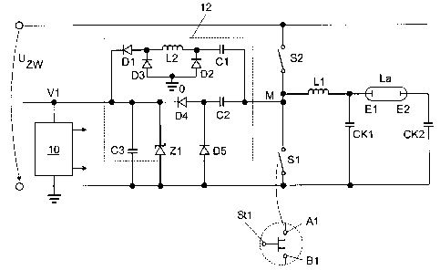
Figure 1 shows a schematic illustration of the detail, which is
relevant to the present invention, of an electronic ballast
according to the invention. In this case, a lamp La is
connected to the center point M of a half-bridge circuit via an
inductance L1, said half-bridge circuit comprising the switches
S1 and S2. Each switch S1, S2 has a working terminal, a
reference terminal and a control input terminal, only the
terminals for the switch S1 being illustrated in the enlarged
CA 02549206 2006-06-O1
2005P04558 US - 6 -
illustration in figure 1, that is to say the working terminal
A1, the reference terminal B1 and the control input terminal
Stl. In the case of the switch S2, the working terminal and
the reference terminal are swapped over in comparison to the
switch S1, i.e. the reference terminal is at the top, the
working terminal is at the bottom, i.e. both working terminals
are connected to the half-bridge center point M. Both
electrodes E1, E2 of the lamp La are connected to the ground
potential, as the reference potential, via coupling capacitors
CK1 and CK2, An auxiliary unit 10, which takes on the function
of driving the two switches S1 and S2, as is expressed by the
two arrows, has a supply terminal V1. A supply unit 12 is
connected between the half-bridge center point M and the supply
terminal V1 of the auxiliary unit 10. It comprises the series
circuit comprising a capacitor C1, an inductance L2 and a first
diode D1. In this case, the capacitor C1 and the inductance L2
form an LC resonant circuit. The connection point between the
inductance L2 and the capacitor C1 is coupled to a reference
potential, in this case a ground potential, via a voltage
limitation apparatus, in this case a diode D2. This diode D2
is used for limiting the voltage step at the connection point
between the capacitor C1 and the inductance L2 to a
predeterminable limit value. The connection point between the
inductance L2 and the diode D1 is likewise coupled to the
reference potential via a diode D3, as a result of which it is
possible to eliminate parasitic oscillations in the supply
signal.
In addition to the supply branch, which comprises the
components C1, D2, L2, D3 and D1, a further supply branch may
be provided between the half-bridge center point M and the
supply terminal V1 of the auxiliary unit 10: for this purpose,
a capacitor C2, also referred to as a so-called snubber
capacitor at this point, is connected to the supply terminal V1
via a diode D4. A diode D5 makes it possible to recharge the
capacitor C2, and a zener diode Z1 is used for limiting the
CA 02549206 2006-06-O1
2005P04558 US - 7 -
voltage to a predetermined value. Moreover, a capacitor C3 may
be provided in order to ensure the supply to the auxiliary unit
of a supply voltage which is as constant as possible.
5 Figure 2 shows a further embodiment of an electronic ballast
according to the invention. In this case, components which
correspond to those in figure 1 are identified by corresponding
reference symbols and will not be described again. This
circuit has an active system input part and is connected on the
10 input side to an AC voltage source 14. The AC voltage signal
is rectified in a rectifier 16, which comprises the diodes D6
to D9, passes through the series circuit comprising an
inductance L3 and a diode D10 and is ultimately provided at a
capacitor C4 as the intermediate circuit voltage UZW of the
half-bridge arrangement having the switches Sl and S2, see also
figure 1 in this regard. For the supply to the auxiliary unit
10, the supply unit 12, which in this case comprises the
capacitor C1, the diodes Dl and D2 and the inductance L2, is
connected to the working terminal of a switch S3. In the
circuit arrangement in figure 2, the switch S3, the diode D10
and the inductance L3 form a boost converter. In this case,
energy is stored in the inductance L3 as long as the switch S3
is closed. Once the switch S3 has opened, this energy is
stored inductively in the output circuit.