Note: Descriptions are shown in the official language in which they were submitted.
CA 02549502 2006-06-05
- 1 -
TITLE OF THE INVENTION
ELECTRONIC DEVICE, POWER SOURCE CONTROL METHOD, ROF
SYSTEM AND. ITS POWER SUPPLYING METHOD AND REMOTE UNIT
BACKGROUND OF THE INVENTION
The present invention relates to an electronic
device of a system for simultaneously operating a
plurality of electronic devices, a power source control
method, a radio over fiber (ROF) system and its power
supplying method and a remote unit.
For instance, when starting up electronic devices
and information processing terminals such as a
plurality of automatic teller machines connected to a
host device in an automatic teller system of a bank,
inrush currents are greatly generated when power is
turned on. And also when television receivers of a
video distribution system, etc., are turned on
simultaneously, rush currents are greatly generated.
Therefore, it is needed for the power source capacity
of the system to be made larger than that of in the
normal operation. And an occurrence of variations in
power also at a primary power source side results in
prevention of a stable operation.
As a measure to deal with foregoing problems, a
conventional system starts up each electronic device in
turn by shifting power supply timings (start up
timings) little by little to each electronic device on
the power supply side of the system then the system
CA 02549502 2006-06-05
- 2 -
suppresses addition and superposition of the rush
currents. For the method of the measure, the video
distribution system employs a method for inserting a
delay line in the middle of a bus line of a power
source supplying power to the television receiver [for
instance, Jpn. Pat. Appln. KOKAI publication
No. 2-295389 (on page 4, FIG. 1)].
In an ROF system, a remote unit power supply
device disposed on a base station side of a cellular
phone supplies power to each remote unit. Each remote
unit having been installed in a distant construction
such as a building or a tower, feeder cables are not
connected through bus lines but laid to each remote
unit from the remote unit power supply device in a
radial pattern. Accordingly, it is impossible to
easily set a delay time only by inserting delay lines
each having the same delay time into the bus line of a
remote unit to be connected next in cascade between
adjacent stations. Therefore, it is needed to manage
complicatedly in such a manner that delay lines
deferring in value for each remote unit have to be
inserted to feeder lines for each remote unit.
In a conventional method, the ROF system has to
manage the remote unit power supply device so as to
supply power with delay times deferring for each
electronic device and television receiver from the
power supplying device side after power is turned on.
CA 02549502 2006-06-05
c
- 3 -
Therefore, the ROF system has a problem that a
complicated management is required and a device scale
is increased.
BRIEF SUMMARY OF THE INVENTION
An object of the present invention is to provide
an electronic device which is easy to manage a power
source to supply power to a plurality of electronic
devices and has small rush currents, a power source
control method, an.ROF system and its power supplying
method and remote unit.
According to an aspect of the present invention,
there is provided an electronic devices to which power
is supplied from a power supplying unit commonly
connected with other electronic devices, each of the
electronic devices comprising: a switch unit having an
input terminal, an output terminal and a control
terminal to which a control signal to close between the
input terminal and the output terminal; a number input
unit to which unique identification information is
input; and a timing unit connected to the power
supplying device together with the input terminal and
inputting the control signal to the control terminal
after a lapse of a delay time set in response to the
identification information from a start timing of power
supplying by the power supplying device.
According to the present invention, an electronic
device which is easy to manage a power turning on
CA 02549502 2006-06-05
- 4 -
timing and also has small rush currents, a power source
control method, an ROF system and its power supplying
method and remote unit can be provided.
Additional advantages of the invention will be set
forth in the description which follows, and in part
will be obvious from the description, or may be learned
by practice of the invention. The advantages of the
invention may be realized and obtained by means of the
instrumentalities and combinations particularly pointed
out hereinafter.
BRIEF DESCRIPTION OF THE SEVERAL VIEWS OF THE DRAWING
The accompanying drawings, which are incorporated
in and constitute a part of the specification,
illustrate embodiments of the invention, and together
with the general description given above and the
detailed description of the embodiments given below,
serve to explain the principles of the invention.
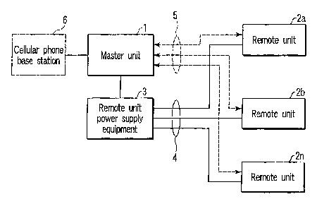
FIG. 1 is an exemplary block diagram showing a
functional configuration of an ROF system of a cellular
phone base station with a power source control method
regarding an embodiment of the invention applied
thereto:
FIG. 2 is an exemplary block diagram showing an
example of a first functional configuration of a remote
unit;
FIG. 3 is an exemplary view of a table explaining
a relationship between an identification number and a
CA 02549502 2006-06-05
i
- 5 -
delay time of a remote unit;
FIGS. 4A and 4B are schematic views showing supply
currents of power supplying devices at start up times
of each remote unit;
FIG. 5 is an exemplary bock diagram showing an
example of a second functional configuration of the
delay control unit;
FIG. 6 is an exemplary block diagram showing an
example of a third functional configuration of the
delay control unit; and
FIG. 7 is an exemplary connection view of a number
input unit and a timing unit when two remote units turn
on at the same timing.
DETAILED DESCRIPTION OF THE INVENTION
(First Embodiment)
FIG. 1 the exemplary block diagram showing the
functional configuration of the radio over fiber (ROF)
system of the cellular phone base station with the
power source control method regarding the embodiment of
the present invention applied thereto. The ROF system
in FIG. 1 includes a master unit 1, remote units 2a-2n
that are electronic devices to be operated by a power
control method of the invention, a remote unit power
supply equipment 3, feeder lines 4 to each remote unit
2a-2n and optical fiber cables 5.
The ROF system is one in which each small-sized
base station having a small output and a cover area,
CA 02549502 2006-06-05
- 6 -
namely each of the remote unit 2a-2n (hereinafter, the
each remote unit 2a-2n will be explained by a remote
unit 2 as a representative thereof unless there is any
need to distinguish each remote unit 2a-2n) operates as
a cellular phone base station. Each remote unit 2a-2n
is connected with a master unit 1 by means of the
optical fiber cable 5 and each remote unit 2 converts
an electric wave to be transmitted and received into an
optical signal to transmit it.
In the ROF system, the remote unit power supply
equipment 3 is connected to each remote unit 2a-2n
through the feeder lines 4 in a radial pattern.
Thereby, it is impossible for the ROF system to adjust
occurrence timings of rush currents at each remote unit
by inserting delay lines in cascade to each feeder line
(power supplying cable) connected to the next remote
unit like the case in which power is supplied
divergingly thorough a bus line.
That is, the master unit 1 is.installed in an
equipment room in a usual building, and each remote
unit 2 is distributed and deposed into its building and
a construction such as adjacent building and a tower.
The remote unit power supply equipment 3 belonging to
the master unit 1 supplies power to each remote unit 2
through the feeder lines 4 laid in a radiation manner
(star-shape). The feeder line has an approximately
several hundred meter at a maximum, so that a delay
CA 02549502 2006-06-05
_ 7 _
time difference caused by a difference of cable lengths
is small. Thereby, when the remote unit power supply
device 2 is turned on, with no difference in power
reception timing (start up timing) of each remote unit
2 that is the power supplying destination, so that rush
currents generated at each remote unit are
superimposed. Accordingly, the ROF system needs to
perform timing control so as not to superimpose the
rush currents by shifting the timing of the power
supplying to each remote unit 2.
FIG. 2 is the block diagram showing the example
of the first functional configuration of the remote
unit 2.
In FIG. 2, the remote unit 2 includes a delay
control unit 211, a switch unit 212, a power source
unit 21 and a radio transmission/reception unit 22. A
power supply (PS) unit 213 is, for instance, a DC/DC
converter. The PS unit 213 may be preferable to be
included in the transmission/reception unit 22;
however, hereinafter, it will be described as if it is
included in the power source unit 21 for the sake of
convenience.
When the remote unit power supply equipment 3 is
turned on, the power source unit 21 controls the timing
to switch on the switch unit 212 from the time point
when the delay control unit 211 started power supplying
(received power) to output a voltage to the PS unit
CA 02549502 2006-06-05
- 8 -
213. The PS unit 213 then outputs prescribed power to
the transmission/reception unit 22. The delay control
unit 211 has a number input unit 2111 composed of a
dial, etc., to input identification information
(number, etc.) of each remote unit 2 and a timing unit
2112 to control a timing to turn on the switch unit 212
in response to the input identification number.
The power which is supplied by the remote unit
power supply equipment 3 to each remote unit 2 is
mainly a DC power source of 100-200V and the following
explanation will be described as an example of a DC
200V power source for the sake of convenience. Even if
other low-voltage DC power source or power source of
100V AC, the timing control to turn on the power source
(power source start) goes same.
Referring to FIG. 2, operations of the remote unit
2 will be set forth. In FIG. 2, each remote unit 2 is
supplied power of 200V DC from a feeder line 4. The
power source of 200V DC is input to the input terminal
of the switch unit 212 and the delay control unit 211.
The delay control unit 211, as a first example,
has a resister R1 and a resister R2 for voltage
dividing, a dial switch S that is a number input unit
2111, and a timing unit 2112 having resisters R10-R19
connected to switching terminals ('1'-'10') of the dial
switch S and a capacitor C connected to a common
connection side of the resisters R10-R19. These
CA 02549502 2006-06-05
_ g _
resisters R10-R19 and the capacitor C consists of an
integration circuit and the output from the integration
circuit is output to a control terminal Co of the
switch unit 212, as a control signal.
At the switch unit 212, the voltage of the input
control signal increases with the time constant of the
integration circuit. And at the timing when the
voltage becomes a prescribed voltage, the switch unit
212 turns on. The output terminal Out of the switch
unit 212 supplies a voltage of 200V DC to the PS unit
(DC/DC converter) 213 to start up the remote unit 2.
The voltage divided by the resister R1 and the
resister R2 may be set, for example, to 5V when using
an FET switch which is turned on at 3-5V of a gate
voltage for the switch unit 212. To obtain a desired
divided voltage, here, a voltage of 5V, a low-voltage
diode may be used in stead of resisters.
Unique identification information (a sequence of
numbers, for instance, '1' for a remote unit 2a, '2'
for a remote unit 2b) is added though the ROF system in
advance, and the sequence of numbers and each switching
terminal ('1', '2', etc.) are matched with one another.
The dial switch S may be one, for example, to match
with the identification numbers displayed on a panel by
a rotary switch, or may be one to specify numbers
displayed on a display window like a thumb wheel
switch.
CA 02549502 2006-06-05
- 10 -
FIG. 3 is a table explaining a relationship
between an identification number and a delay time of a
remote unit. In FIG. 3, '1' is added to the remote
unit 2a as an identification number to be input-set by
the number input unit 2111 (dial switch S). The
resistor R10 (a resistor of resistance value of 10 KSZ)
is connected to a switching terminal corresponding to
'1' of the dial switch S. Similarly, identification
numbers of numbers '2'-'10' are added in sequential
numbers to the remote unit 2a-2k, respectively, and
resistors R11-R19 having resistance values which are
each 10 KS~ larger at every switching terminal are
connected to each switching terminal of each number,
respectively: The other ends of each resistor R10-R19
are connected to the capacitor C of 10 ,u F commonly.
At the remote unit 2a of which the identification
number is '1', the resistor R10 selected by the dial
switch C consists of an integration circuit together
with the capacitor C and a raising time (time constant)
of 700 of a final reaching voltage becomes
120 millisecond (millisecond). Similarly, at the
remote unit 2k of which the identification number is
'10', the resistor R19 having been selected, the
raising time becomes 1204 millisecond.
The timing unit 2112 setting raising times (delay
times) of each remote unit 2 adjusts, as shown in
FIG. 2, the time constant of the integration circuit by
CA 02549502 2006-06-05
- 11 -
switching the resistors R10-R19. In stead of this, the
timing unit 2112, of course, may adjust the delay times
of the integration circuit by changing the capacitor C
while maintaining the value of resistors R10-R19
constant.
For instance, at the delay control unit 211 of the
remote unit 2a, the elapse of 120 millisecond after the
start of power supplying from the remote unit power
supply equipment 3, a voltage of 5X0.7=3.5V needed for
the switch unit 212 to turn on is obtained. Here, the
voltage of 200V DC is applied to the PS unit 213 to
start up the remote unit 2a and a transient phenomenon
accompanying power supplying occurs to pass rush
currents.
FIG. 4A and FIG. 4B are schematic views showing
supply currents from the remote unit power supply
equipments 3 at the start up times of each remote unit
2. FIG. 4A shows the case in which delay times are not
set to each remote unit 2 but each remote unit 2 starts
up immediately after power supplying from the remote
unit power supply equipment 3. In this case, when n
sets of remote units 2a-2n are turned on
simultaneously, the rush current becomes n times at the
time when the supply current reaches a peak (for
example, 60 millisecond after turning on).
In contrast, in the first embodiment, delays in
start up timing of each remote unit 2 are provided,
CA 02549502 2006-06-05
- 12 -
respectively, as shown in FIG. 4B. For example, a
delay time after power supplying is not set on the
remote unit 2a and a delay time of 60 millisecond is
set on the timing at which the switch unit 212 of the
remote unit 2b is tuned on.
In this case, the timing at which the rush current
of the remote unit 2b reaches a peak becomes a time
point with further 60 millisecond passed thereto after
the rush current of the remote unit 2a reached the peak
(120 millisecond after turning on the remote unit power
supply equipment 3). At this time point, the rush
current of the remote unit 2a has passed the peak to
decrease toward a steady-state value. Therefore, at
this time point, the current supplied from the remote
unit power supply equipment 3 becomes a value lower
than the value that is made twice as large as the rush
currents at every one set of the remote units 2.
More specifically, the delay time at which each
remote unit 2 is turned on, namely, switch unit 212
turns on is made longer than the time at which the rush
current of each remote unit 2 reaches the peak (wherein
60 millisecond). Furthermore, the remote unit 2 sets
the time constant of the timing unit 2112, namely the
integration circuit so that the delay times set to each
remote unit 2 become longer that the peak reaching
time. Thereby, the remote unit 2 can prevent the
current supplied from the remote unit power supply
CA 02549502 2006-06-05
- 13 -
equipment 3 becoming n times of the rush current of one
set of the remote unit 2.
Especially, as shown in FIG. 4B, if the start up
timing is set so that the remote unit 2d is turned on
after termination of a rush current, influence of the
rush current is further reduced. Thereby, the remote
unit 2 can reduce the supply current capacity of the
remote unit power supply equipment 3 and suppress load
variations on the primary power source.
As mentioned above, like this embodiment, the ROF
system can avoid superimposing the rush currents
without having to make the remote unit power supply
equipment 3 control the power source start up timings
for each remote unit 2.
(Second Embodiment)
FIG. 5 is an example of a second configuration of
the remote unit 2. In FIG. 5, a vernier dial D is used
for the number input unit 2111 of the delay control
unit 211. The timing unit 2112 has a potentiometer Rp
and a capacitor C which are combined with the vernier
dial D. The vernier dial D can display a resistance
division ratio of the potentiometer Rp in response to a
rotary ratio of the vernier dial D. For instance, if
remote unit numbers are assigned by a dial memory at
every time to divide equally into ten, the time
constant can be adjusted in a similar way in a dial
switch S like the thumb wheel switch.
CA 02549502 2006-06-05
- 14 -
That is to say, it is presumed that the number of
the sets of the remote units is 10 and the
potentiometer Rp of 100 KS2 is in use. The ROF system
then adds the number 10 to the remote unit 2a and
matches the scale of the vernier dial D with 10. The
ROF system further adds the number 20 to the remote
unit 2b and matches the scale of the vernier dial D
with 20. Thereby, at every increase by 10 in the
number (every memory position to be divided equally
into 10), the resistance value of the potentiometer Rp
increases by 10 KS2. Therefore, like the case of use
of the dial switch S, the ROF system can set the timing
at every around 120 millisecond.
The setting of equal divisions into 100 by the
scale of the vernier dial D enables fitting also to set
two-digit identification information (number). For
instance, for using a potentiometer of 1 MSZ,
resistance values of 10 KS2 steps which are divided
equally into 100 are combined with a capacitor C of
10 ,uF then delay times in units of around
120 millisecond can be set.
(Third Embodiment)
FIG. 6 is an example of a third configuration of
the delay control unit 211. In this example, the delay
control unit 211 has the dial switch S at the number
input unit 2111. The timing unit 2112 has a timer IC
214 and the resistors R10-R19. The timer IC 214
CA 02549502 2006-06-05
- 15 -
outputs a voltage of, for example, 5V required by the
switch unit 212. Adding this voltage brings the switch
unit 212 into an on state. A DC power source voltage-
divided by the resistors R1 and R2 is connected to the
timer IC 214.
In this third embodiment, the delay control unit
211 controls the start up timing of the remote unit 2
by connecting the time constant circuit composed of the
resistors R10-R19 and the capacitor C to timing setting
terminals of the timer IC 214. The delay control unit
211 outputs a switch control signal of 5V to the switch
unit 212 from the timer IC 214 at the same timings as
those of the first and second embodiments.
With respect to setting methods of delay times,
methods other than above-mentioned methods may be used
appropriately. The essential point of the present
invention is to each provide an input means of the
identification information (number, etc.) and a delay
control means for setting the delay times (time
constants) corresponding to the identification
information for each remote unit 2 (namely, electronic
device or its power source device).
If the rush current at turning on the power source
of the remote unit 2 does not become larger than a
consumption current in a steady-state operation, the
delay control unit 211 may be configured to make a
plurality of remote units 2 turn on at the same timing.
CA 02549502 2006-06-05
- 16 -
FIG. 7 is the exemplary connection view of the
number input unit and the timing unit when two sets of
the remote units 2 turn on at the same timing. In the
remote unit 2 in FIG. 7, a switch terminal of the dial
switch S, for example, '1' is connected to the common
resistor R21 so that two sets of the remote units 2
turn on simultaneously. Also with respect to other
remote units 2, the resistors R22-R25 are connected to
the dial switch S so that each pair of two sets thereof
turns on at the same timing.
As described above, on the side of the remote unit
power supply equipment 3, there is no need for each
remote unit 2 to manage the timing to turn on. And
also the method is simple, in which the remote unit 2
self-monitors the power supply voltage to control a
timing of switch closing. Therefore, a power source
control method and an electronic device for suppressing
the rush currents in the ROF system can be achieved at
ease and low costs.
The power source control method of the present
invention is not limited to the ROF system, the method
is applicable to the systems to be used by being
combined with a plurality of electronic devices as
described above and it goes without saying that the
method is also applicable to the electronic devices.
Additional advantages and modifications will
readily occur to those skilled in the art. Therefore,
CA 02549502 2006-06-05
- 17 -
the invention in its broader aspects is not limited to
the specific details and representative embodiments
shown and described herein. Accordingly, various
modifications may be made without departing from the
spirit or scope of the general inventive concept as
defined by the appended claims and their equivalents.