Note: Descriptions are shown in the official language in which they were submitted.
CA 02549721 2006-06-08
- 1 - 2005P07771US-RAI
Circuit arrangement and method for driving a gate of a
transistor, in particular a MOSFET
Technical field
The present invention relates to a circuit arrangement for
driving a gate of a transistor, in particular a MOSFET. The
invention also relates to a method for driving a gate of such a
transistor.
Prior art
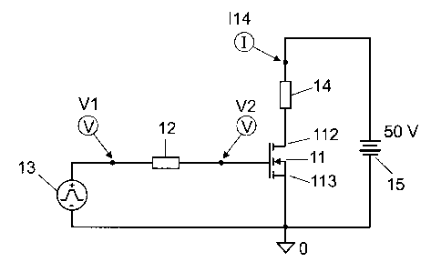
Circuit arrangements for driving gates of transistors are
known. Such a known circuit arrangement is illustrated in
figure 1. The circuit arrangement 1 comprises a MOS transistor
11, which is electrically connected with its gate 111 to a gate
series resistor 12. The gate series resistor 12 is electrically
connected to a pulsed DC voltage source 13. As can further be
seen in figure 1, the drain terminal of the MOS transistor 11
is connected to a load resistor 14, this load resistor 14 being
electrically connected to a voltage source 15. Furthermore, the
source terminal 113 of the MOS transistor 11 is connected to
ground potential. The circuit arrangement 1 illustrated in
figure 1 is arranged in an electronic ballast, which is used
for operating and adjusting fluorescent lamps.
Figure 2 shows three different signal profiles V1, V2 and I,
which are tapped off at points V1, V2 and I in figure 1. As can
be seen in this case in figure 2, the signal profile V1
characterizes a digital voltage profile. The signal profile V2
characterizes the voltage profile at the gate 111 of the MOS
transistor 11. Furthermore, the illustration in figure 2
CA 02549721 2006-06-08
- 2 - 2005P07771US-RAI
represents the signal profile I, which characterizes the
current profile through the load resistor 14.
As can be seen from the illustration in figure 2, the gate
series resistor 12 is switched over from 100 ohms to 400 ohms
at time t=55 ~s. As can be seen in this case, the signal
profile V2 at the gate 111 of the transistor 11 is thus altered
and, as a result, the edge steepness of the load current
through the load resistor 14 is altered directly, in accordance
with the signal profile I. Owing to the change in the switching
speed, two opposing properties can be seen. On the one hand,
when the resistance value of the gate series resistor 12 is
reduced, the switching losses in the circuit arrangement 1 are
likewise reduced. However, when there is such a reduction in
the resistance value of the gate series resistor 12, the
electromagnetic interference (EMI) is increased. When the
resistance value of the gate series resistor 12 is increased,
the switching losses of the circuit arrangement 1 are
increased, in which case the electromagnetic interference is
reduced. In practice, it was now possible also to observe the
fact that the permissible EMI limit values of an electronic
operating device, which is represented, for example, by the
HTi DALI 150/220-240 DIM, are not exceeded at dimming settings
of the electronic ballast which are substantially greater than
1% of a maximum dimming setting. However, if dimming settings
are set which are approximately in the range between 0.1% and
1%, it was possible to establish that the permissible limit
values for the electronic converter are being exceeded.
In order to counteract such a case of the permissible limit
values being exceeded, in particular at the abovementioned
dimming settings, an increase in the gate series resistance was
set, as a result of which the EMI response can be improved at
all dimming settings. One significant disadvantage with such a
procedure, however, is the fact that the power loss is
increased at all dimming settings. This in turn leads to
relatively high losses in the overall embodiment of an
CA 02549721 2006-06-08
- 3 - 2005P07771US-RAI
electronic device, in which such a MOS transistor having such a
drive circuit is arranged. For example, it is thus necessary
for the housing in which the circuit arrangement, in particular
the transistor, is arranged to be designed to be larger or for
the permissible ambient temperature to be reduced.
Summary of the invention
The present invention is therefore based on the object of
providing a circuit arrangement and a method for driving a gate
of a transistor, with which circuit arrangement and with which
method it is possible to overcome the disadvantages of the
prior art. In particular, the intention is to achieve a
situation in which an improved EMI response can be ensured at
all dimming settings and an appropriate adjustment of the power
loss can be achieved.
This object is achieved by a circuit arrangement which has the
features in accordance with patent claim 1. Furthermore, this
object is achieved by a method which has the features in
accordance with patent claim 8.
A circuit arrangement according to the invention is designed
for driving a gate of a transistor, which is, in particular, a
MOSFET, the transistor being arranged in an electronic device.
One essential concept of the invention consists in the fact
that the circuit arrangement is designed for variably driving
the gate of the transistor as a function of the operating state
of the electronic device, in which the transistor is used. This
makes it possible to achieve a situation in which the power
loss can be altered or influenced individually and precisely
and losses now only need to be increased in the region in which
they are required. The invention can be used to optimize the
EMI response at all dimming settings in particular when the
circuit arrangement according to the invention is arranged in
an electronic ballast. Variable driving of the gate as a
function of the operating state of the electronic device makes
CA 02549721 2006-06-08
- 4 - 2005P07771US-RAI
it possible to set the power loss at all dimming settings
depending on the situation and therefore in an efficient and
effective manner.
The circuit arrangement advantageously comprises a control
unit, which is designed for variably driving the gate of the
transistor, the circuit arrangement furthermore also having a
gate driver circuit, which can be electrically connected to the
control unit (low-side driver) or else has electrical isolation
- magnetic or optical or capacitive - for the purpose of
driving an upper transistor in a half-bridge arrangement
(high-side driver) and can be parameterized by the control
unit, the gate driver circuit being electrically connected to
the gate of the transistor. The implementation of the circuit
arrangement according to the invention is thus relatively low
in complexity and has a space-saving design.
The gate driver circuit is preferably connected between the
control unit and the gate of the transistor. In this case, the
control unit is designed for transmitting a gate driving signal
and a parameterization signal to the gate driver circuit. The
control unit, which is preferably in the form of a
microprocessor, is thus designed for transmitting two separate
signals, the gate driving signal and the parameterization
signal.
In one advantageous embodiment, the gate driver circuit has an
external, fixed gate series resistor and is furthermore
designed such that pulse-width modulation, in particular
dynamic pulse-width modulation, of the output signal of the
gate driver circuit can be carried out at the output of the
gate driver circuit. A pulse-width-modulated output signal can
thus be provided at the output of the gate driver circuit and
can be applied to the gate of the transistor via the external
gate series resistor.
CA 02549721 2006-06-08
- 5 - 2005P07771US-RAI
In one further advantageous refinement of the invention, the
gate driver circuit has an external, fixed gate series resistor
and is designed such that an analog-controlled output signal
can be provided at the output of the gate driver circuit . The
gate driver circuit may preferably have an internally
controlled series resistor. With such an implementation, it is
thus possible to provide for the arrangement of one or more
series resistors and/or current sources in a substrate in a
semiconductor component, in which case these internal and
controlled series resistors lead to a common terminal, which
may advantageously be connected directly to the gate of the
transistor to be driven.
In one particularly preferred refinement, the gate driver
circuit has a circuit which is graduated in binary fashion and
comprises pull-up resistors and pull-down resistors. The
pull-up/pull-down resistor combination which is graduated in
binary fashion may advantageously have an IzC interface, it
being possible for provision to be made for the configuration
register to be updated only in the event of a necessary change
to the values stored therein.
In one method according to the invention for driving a gate of
a transistor, which is in particular in the form of a MOSFET,
and in which the transistor is arranged in an electronic
device, the gate of the transistor is driven in variable
fashion as a function of the operating state of this electronic
device. The method according to the invention can thus make it
possible for a power loss to be altered, as required, and only
to be altered in situations in which this is necessary.
Furthermore, with the method according to the invention, which
is advantageously carried out in an electronic ballast, it is
possible to achieve a situation in which the EMI response can
be positively influenced at all dimming settings when setting
dimming settings of the electronic ballast. With the method
according to the invention, which is carried out in an
electronic ballast, it is thus also possible to achieve a
CA 02549721 2006-06-08
- 6 - 2005P07771US-RAI
situation in which the power loss at all dimming settings can
be adjusted, in particular increased, effectively and
efficiently as a function of the correspondingly present
situation.
Brief description of the drawings
One exemplary embodiment of the present invention will be
explained in more detail below with reference to schematic
drawings, in which:
figure 1 shows a circuit arrangement known from the prior
art for driving a gate of a transistor;
figure 2 shows signal profiles of signals of the circuit
arrangement shown in figure 1;
figure 3 shows a block circuit diagram of a circuit
arrangement according to the invention; and
figure 4 shows a further illustration of the circuit
arrangement according to the invention shown in
figure 3.
Preferred embodiment of the invention
Figure 3 shows a simplified block circuit diagram of a circuit
arrangement 2 according to the invention. The circuit
arrangement 2 comprises a control unit, which in the exemplary
embodiment is in the form of a microprocessor 21. Furthermore,
the circuit arrangement 2 comprises a gate driver circuit 22.
As can be seen from the illustration in figure 3, the
microprocessor 21 is electrically connected to the gate driver
circuit 22, the microprocessor 21 being designed for
transmitting a gate driving signal 211. The microprocessor 21
is designed for transmitting a parameterization signal 212 to
the gate driver circuit 22 via a further signal connection
CA 02549721 2006-06-08
- 7 - 2005P07771US-RAI
formed in the exemplary embodiment. The gate driver circuit 22
is connected to a transistor, which in the exemplary embodiment
is in the form of a MOSFET 23. The electrical connection of the
gate driver circuit 22 is in this case formed in particular
with the gate of the MOSFET 23.
As can already be seen in the illustration in figure 3, the
circuit arrangement 2 according to the invention is designed
for variably driving the gate of the MOSFET 23. In the process,
the microprocessor 21 produces both signals, by means of which
the operating state of the MOSFET 23 is characterized, and also
signals, by means of which parameterization of the gate driver
circuit 22 can be carried out. The illustration of the
invention shown in figure 3 can be used to ensure control of
the power loss such that losses are only increased in the
region where this is necessary. It is thus no longer necessary
in a case in which the circuit arrangement 2 is arranged in an
electronic ballast for the power loss to be increased across
the board at all dimming settings . Owing to the invention, it
is thus possible for such an increase in the power loss for
specific dimming settings to be carried out depending on the
situation and individually.
Figure 4 shows a further illustration of the circuit
arrangement 2 according to the invention shown in figure 3. As
can be seen here, further elements are illustrated in the
respective units of the circuit arrangement 2. The gate driver
circuit 22 has storage registers, in which states determined by
bits stored therein fox the transistors associated with the
respective storage cell can be realized. In the exemplary
embodiment, the gate driver circuit 22 in this case has a
register having four bits for the configuration of four npn
transistors or bipolar switching transistors 222a to 222d
having four collector resistors or pull-down resistors 223a to
223d which are advantageously graduated in binary fashion. In
this case, the register is characterized by the bits L BITO to
L BIT3. In a corresponding manner, the gate driver circuit 22
CA 02549721 2006-06-08
- 8 - 2005P07771US-RAI
comprises a register, which contains the bits H BITO to H BIT3
for the configuration of four pnp transistors or bipolar
switching transistors 225a to 225d having four collector
resistors or pull-up resistors 226a to 226d, which are
advantageously graduated in binary fashion.
Furthermore, the microprocessor 21 comprises a unit for
producing the gate driving signal 211, and an interface IzC for
transmitting the parameters 212 for the gate driver circuit 22,
said parameters being stored in the corresponding configuration
register. Owing to the bits L BITO to L BIT3 and H BITO to
H BIT3, it is thus possible for signals to be produced by the
microprocessor 21, and these signals are used for
parameterizing the gate driver circuit 22.
As can be seen from the illustration in figure 4, the gate
driver circuit 22 has four AND elements 221a to 221d. The gate
driving signal 211 produced by the unit arranged in the
microprocessor 21 is in each case applied, inverted, to a first
input 1 of the AND elements 221a to 221d. Furthermore, a signal
connection to the configuration register having the bit L BITO
is formed at a second input 2 of the first AND element 221a. In
a corresponding manner, electrical connections between second
inputs 2 of the AND elements 221b to 221d and the configuration
register having the bits L BITl to L BIT3 are formed.
Each of the outputs 3 of the AND elements 221a to 221d is in
this case connected to in each case one of the bipolar
switching transistors 222a to 222d. As can be seen from the
illustration in figure 4, the outputs 3 of these AND elements
221a to 221d are electrically connected to the base terminals
of these bipolar switching transistors 222a to 222d. These
bipolar switching transistors 222a to 222d are each connected
to ground potential with their emitter terminal. The collector
terminal of the switching transistor 222a is electrically
connected to a first pull-down resistor 223a, the connector
terminal of the switching transistor 222b is electrically
CA 02549721 2006-06-08
- 9 - 2005P07771US-RAI
connected to a second pull-down resistor 223b, the collector
terminal of the switching transistor 222c is electrically
connected to a third pull-down resistor 223c, and the collector
terminal of the switching transistor 222d is electrically
connected to a fourth pull-down resistor 223d.
As can be seen in figure 4, the four pull-down resistors 223a
to 223d are graduated in binary fashion and, in the exemplary
embodiment, have resistance values of 256 ohms and 128 ohms and
64 ohms and 32 ohms, respectively. The four pull-down resistors
are electrically connected to a gate 221 of the MOSFET 23.
Furthermore, the gate driver circuit 22 in the exemplary
embodiment comprises four inverting AND elements (NAND) 224a to
224d, the gate driving signal 211 produced by the unit of the
microprocessor being applied to first inputs 1 of these NAND
elements 224a to 224d. Furthermore, an electrical connection is
formed between a second input of the NAND element 224a and the
configuration register having the bit H BITO. In a
corresponding manner, electrical connections are formed between
the second inputs of the further NAND elements 224b to 224d and
the configuration register having the bits H BIT1 and H BIT2
and H BIT3, respectively. As can further be seen in figure 4,
the outputs 3 of the NAND elements 224a to 224d are each
electrically connected to a base terminal of a bipolar
switching transistor 225a to 225d. The bipolar switching
transistors 225a to 225d are electrically connected with their
emitter terminals to a voltage source 24. The collector
terminal of the bipolar switching transistor 225a is
electrically connected to a first pull-up resistor 226a, the
collector terminal of the bipolar switching transistor 225b is
electrically connected to a second pull-up resistor 226b, the
collector terminal of the bipolar switching transistor 225c is
electrically connected to a third pull-up resistor 226c and the
collector terminal of the bipolar switching transistor 225b is
electrically connected to a fourth pull-up resistor 226d. The
four pull-up resistors 226a to 226d are graduated in binary
CA 02549721 2006-06-08
- 10 - 2005P07771US-RAI
fashion and, in the exemplary embodiment, have resistance
values of 256 ohms and 128 ohms and 64 ohms and 32 ohms,
respectively. Furthermore, these four pull-up resistors 226a to
226d are electrically connected to the gate 221 of the MOSFET
23.
The "low" bits L BITO to L BIT3 are designed to isolate the
pull-down resistors 223a to 223d. In a corresponding manner,
the "high" bits H BITO to H BIT3 are designed to isolate the
associated pull-up resistors 226a to 226d. As is illustrated in
the exemplary embodiment of the invention shown in figure 4,
the gate 221 of the MOSFET 23 can be driven in variable fashion
by the circuit arrangement 2 as a function of the operating
state of said MOSFET 23 by means of the microprocessor 21 and
the gate driver circuit 23.
When the graduated resistors shown in figure 4 are implemented
internally and thus the resistors are formed in a semiconductor
substrate, it is possible for the maximum possible time
constants to be matched by means of a capacitor additionally
being connected in parallel with the gate 221 of the MOSFET 23.