Note: Descriptions are shown in the official language in which they were submitted.
CA 02549892 2006-06-12
ELECTRICAL CONNECTOR AND SYSTEM FOR A COMPONENT IN AN
ELECTRONIC DEVICE
FIELD OF THE INVENTION
[0001] The invention described herein relates to a connector used in a
handheld
electronic device. In particular, the invention described herein relates to a
connector for a
component, such as a LCD display, used in an electronic device, such as a
compact
handheld electronic device.
BACKGROUND
[0002] The conventional handheld electronic device, such as a PDA, or a
wireless
telephone, includes a keyboard/keypad, a display and a system printed circuit
board
(PCB) disposed within a common housing. The display is typically provided as a
reflective, transmissive or transreflective LCD display panel.
[0003] To limit power losses and the effects of noise on the system, the LCD
display
electronics must be disposed in close proximity to the LCD display panel.
Accordingly,
the LCD display electronics are provided on a flexible printed circuit board
that is housed
within a plastic or metal support frame with the LCD display panel. The frame
is then
fixedly attached to the PCB using known techniques and devices, such as
permanent
adhesive, clips, screws or snaps. Alternatively, the display panel may be
loosely set in its
final position on the PCB, when the housing is closed over the PCB and the
display
panel, internal elements in the housing press onto the display panel to keep
it fractionally
held against the PCB.
-1-
CA 02549892 2006-06-12
[0004] To prevent the display electronics from making contact with electronics
and
tracks on the PCB, the frame maintains a small gap between the display
electronics on the
PCB and the electronics on the PCB. However, this design increases the
thickness of the
electronic device. For instance, in the conventional handheld electronic
device, a gap of
approximately 1.5 mm is preferably maintained between the display electronics
and the
PCB electronics (1.2 mm for the height of the display electronics; and an
additional 0.3
mm for the clearance between the display electronics and the PCB electronics).
[0005] In the case of a wireless-enabled electronic device, typically the
antenna and RF
electronics are disposed near the uppermost end of the electronic device to
avoid
attenuation of the RF signal by the user's hand as the user holds the device.
Since this
position for the RF electronics within the housing coincides with that of the
display, the
gap between the display electronics and the PCB electronics must be decreased.
This
latter design further increases the need to reduce the gap between the LCD and
PCB.
[0006] Therefore, there is a need for a configuration of components in a
handheld
electronic device that allows the thickness of the device to be reduced.
SUMMARY
[0007] In a first aspect of an embodiment, an electronics connection system
for an
electronic device is provided. The system comprises a printed circuit board
(PCB)
having a top side, a bottom side and an edge between the top side and the
bottom side;
and a connector for making an electrical connection with an electronic device.
In the
device, an electrical pad is located on its bottom side. The electronic device
is mountable
to the top side of the PCB. Also, the connector is connectable to a connection
pad on the
PCB which is not on the top side of the PCB.
-2-
CA 02549892 2006-06-12
[0008] In the system, when the electronic device is mounted on the PCB in its
final
location, the connector may not be bent inbetween the bottom of the electronic
device
and the top of the PCB.
[0009] In the system, the connector may move from a first position to a second
position
as the electronic device is mounted to the top of the PCB. When in the second
position,
the connector may be biased towards the first position and an end portion of
the
connector may be in electrical contact with the electrical pad of the
electronic device.
[0010] In the system, the connector may be connected to the connection pad via
a solder
connection or a welded connection.
[0011] In the system, the end portion of the connector may be a curved tip.
[0012] In the system, the connection pad may be located on the bottom side of
the PCB.
[0013] In the system, the connection pad may be located on an edge of the PCB.
[0014] Alternatively, in the system, the connection pad may be located on the
bottom
side of the PCB; the connector may route around an end of the PCB; and the
connector
may move from a first position to a second position as the electronic device
is mounted to
the top of the PCB. When in the second position, the connector is biased
towards the first
position and an end portion of the connector is in electrical connection with
the electrical
pad of the electronic device.
[0015] In a second aspect, an electronics module for an electronic device is
provided.
The module comprises: a PCB having a top side, a bottom side and an edge
between the
top side and the bottom side; an electronic device having a flexible
connector, the
electronic device being mountable to the top side of the PCB; and a second
connector for
-3-
CA 02549892 2006-06-12
receiving the first connector. On the PCB, the connector is located on either
the bottom
side or the edge of the PCB.
[0016] In the module, the electronic device may be mounted on the PCB and the
flexible
connector is not bound between a bottom of the display and the top of the PCB.
[0017] In the module, the PCB may comprise a cavity from the top side to the
bottom
side. Further, the flexible connector may be routed through the cavity from
the display to
the second connector.
[0018] In the module, the second connector may be located on the bottom side
of the
PCB.
[0019] In the module, the flexible connector may be biased at its distal end
towards the
second connector.
[0020] In the module, the second connector may be a solder pad.
[0021] Alternatively, in the module, the second connector may be located on an
edge of
the cavity of the PCB.
[0022] In other aspects various combinations of sets and subsets of the above
aspects are
provided.
BRIEF DESCRIPTION OF THE DRAWINGS
[0023] The invention will now be described, by way of example only, with
reference to
the accompanying drawings, in which:
[0024] Fig. 1 is a front plan view of a handheld electronic device which
provides a
housing for embodiments of the invention described herein;
-4-
CA 02549892 2006-06-12
[0025] Fig. 2 is a schematic view depicting functional details of the handheld
electronic
device of Fig. 1, including a communication subsystem and a LCD
display;
[0026] Fig. 3 is an upper perspective view of a printed circuit board (PCB) of
the
handheld electronic device of Fig. 1, depicting the location of the
communication subsystem shown in Fig. 2;
[0027] Fig. 4 is a rear perspective view of the LCD display of the handheld
electronic
device of Fig. 2;
[0028] Fig. 5 is upper perspective view of the LCD display of Fig. 4 secured
to the PCB
of Fig. 3;
[0029] Fig. 6 is an exploded upper perspective view of the LCD display and PCB
of Fig.
5;
[0030] Fig. 7 is a side view of the LCD display and PCB of Fig. 5;
[0031] Fig. 8 is a bottom perspective view of another embodiment of a PCB and
a
connector for the handheld device of Fig. 1;
[0032] Fig. 9 is a partial side view of yet another embodiment of a PCB and a
connector
for the handheld device of Fig. 1;
[0033] Fig. 10 is an upper perspective view of yet another embodiment showing
another
PCB for the handheld electronic device of Fig. l;
[0034] Fig. 11 is side view of the embodiment of Fig. 10 having a display
mounted
thereto; and
-5-
CA 02549892 2006-06-12
[0035] Fig. 12 is an upper perspective view of yet another embodiment showing
another
PCB and another LCD display for the handheld electronic device of Fig. 1.
DETAILED DESCRIPTION OF AN EMBODIMENT
[0036] The description which follows, and the embodiments described therein,
are
provided by way of illustration of an example, or examples, of particular
embodiments of
the principles of the present invention. These examples are provided for the
purposes of
explanation, and not limitation, of those principles and of the invention. In
the
description, which follows, like parts are marked throughout the specification
and the
drawings with the same respective reference numerals.
[0037] Fig. 1 schematically illustrates a handheld mobile communication device
10 and
its components, including a housing 12, an input device (e.g. keyboard 14) and
an output
device (a display 16), which is preferably a graphic liquid crystal display
(LCD),
although other types of output devices may alternatively be utilized.
Typically, housing
12 is a moulded polycarbonate structure and may be formed via known plastic
injection
moulding techniques. To assist in assembly of device 10, housing 12 typically
comprises
two or more pieces which fit together in a fitted arrangement to enclose the
internal
devices and form an exterior casing for device 10. For example, housing 12 may
comprise an upper housing and a lower housing. Physically for device 10,
housing 12
may be elongated vertically, or may take on other sizes and shapes (including
clamshell
housing structures).
[0038] Referring to Fig. 2, a processing device (a microprocessor 18) is shown
schematically as coupled between keyboard 14, display 16 and a series of other
internal
devices to device 10. The microprocessor 18 controls the operation of the
display 16, as
-6-
CA 02549892 2006-06-12
well as the overall operation of the device 10, in response to actuation of
keys on the
keyboard 14 or thumbwheel by a user. Exemplary microprocessors for
microprocessor
18 include Data 950 (trade-mark) series microprocessors and the 6200 series
microprocessor, both available from Intel Corporation.
[0039] In addition to the microprocessor 18, other internal devices of the
device 10 are
shown schematically in Fig. 2. These devices include: a communication
subsystem 100,
a short-range communication subsystem 102, a set of auxiliary I/O devices 106,
a serial
port 108, a speaker 110 and a microphone 112. Memory for device 10 is provided
in
flash memory 116 and Random Access Memory (RAM) 118. Internal devices are
enclosed within housing 12 and typically are either mounted onto a printed
circuit board
(PCB), affixed to an interior part of the housing or suspended by some means
within
housing 12.
[0040] The device 10 is preferably a two-way radio frequency (RF)
communication
device having voice and data communication capabilities. In addition, device
10
preferably has the capability to communicate with other computer systems via
the
Internet.
[0041] Operating system software executed by the microprocessor 18 is
preferably stored
in a computer readable medium, such as flash memory 116, but may be stored in
other
types of memory devices, such as read only memory (ROM) or similar storage
element.
In addition, system software, specific device applications, or parts thereof,
may be
temporarily loaded into a volatile store, such as RAM 118. Communication
signals
received by the mobile device may also be stored to RAM 118.
CA 02549892 2006-06-12
[0042] Microprocessor 18, in addition to its operating system functions,
enables
execution of software applications on device 10. A set of software
applications that
control basic device operations, such as a voice communication module 130A and
a data
communication module 130B, may be installed on the device 10 during
manufacture or
S downloaded thereafter. Cell mapping module 130C may also be installed on
device 10
during manufacture. As well, additional software modules, illustrated as an
other
software module 130N, which may be, for instance, a personal information
manager
(PIM) application, may be installed during manufacture or downloaded
thereafter into
device 10. PIM application is preferably capable of organizing and managing
data items,
such as e-mail messages, calendar events, voice mail messages, appointments,
and task
items. PIM application is also preferably capable of sending and receiving
data items via
a wireless network 140.
[0043] Communication functions, including data and voice communications, are
performed through the communication subsystem 100, and possibly through the
short-
range communication subsystem 102. Communication subsystem 100 includes
receiver
150, transmitter 152 and one or more antennae, illustrated as receive antenna
154 and
transmit antenna 156. In addition, communication subsystem 100 also includes
processing module, such as digital signal processor (DSP) 158 and local
oscillators (LOs)
160. The specific design and implementation of communication subsystem 100 is
dependent upon the communication network in which device 10 is intended to
operate.
For example, communication subsystem 100 of the device 10 may be designed to
operate
with the Mobitex (trade-mark), DataTAC (trade-mark) or General Packet Radio
Service
(GPRS) mobile data communication networks and also designed to operate with
any of a
_g_
CA 02549892 2006-06-12
variety of voice communication networks, such as Advanced Mobile Phone Service
(AMPS), Time Division Multiple Access (TDMA), Code Division Multiple Access
CDMA, Personal Communication Service (PCS), Global System for Mobile
Communication (GSM), etc. Other types of data and voice networks, both
separate and
integrated, may also be utilized with device 10. It will be appreciated that
some signals
received and transmitted through the subsystem 100 may provide interfering
signals with
other components in device 10, such as microphone 112.
[0044] Network access requirements vary depending upon the type of
communication
system which can communicate with device 10. For example, in the Mobitex
(trade-
mark) and DataTAC (trade-mark) networks, mobile devices are registered on the
network
using a unique Personal Identification Number (PIN) associated with each
device. In
GPRS networks, however, network access is associated with a subscriber or user
of a
device. A GPRS device therefore requires a subscriber identity module,
commonly
referred to as a Subscriber Identity Module (SIM) card, in order to operate on
a GPRS
network.
[0045] When required network registration or activation procedures have been
completed, device 10 may send and receive communication signals over
communication
network 140. Signals received from communication network 140 by the receive
antenna
154 are routed to receiver 150, which provides for signal amplification,
frequency down
conversion, filtering, channel selection, etc., and may also provide analog to
digital
conversion. Analog-to-digital conversion of received signals allows the DSP
158 to
perform more complex communication functions, such as signal demodulation and
decoding. In a similar manner, signals to be transmitted to network 140 are
processed
-9-
CA 02549892 2006-06-12
(e.g., modulated and encoded) by DSP 158 and are then provided to transmitter
152 for
digital to analog conversion, frequency up conversion, filtering,
amplification and
transmission to communication network 140 (or networks) via the transmit
antenna 156.
[0046] In addition to processing communication signals, DSP 158 provides for
control of
receiver 150 and transmitter 152. For example, gains applied to communication
signals
in receiver 150 and transmitter 152 may be adaptively controlled through
automatic gain
control algorithms implemented in DSP 158.
[0047) In a data communication mode, a received signal, such as a text message
or web
page download, is processed by the communication subsystem 100 and is input to
microprocessor 18. The received signal is then further processed by
microprocessor 18
for an output to the display 16, or alternatively to some other auxiliary I/O
devices 106.
A device user may also compose data items, such as e-mail messages, using
keyboard
(keypad) 14, and/or some other auxiliary I/O device 106, such as a touchpad, a
thumb-
wheel, a rocker switch or some other type of input device. The composed data
items may
then be transmitted over communication network 140 via communication subsystem
100.
[0048] In a voice communication mode, overall operation of device 10 is
substantially
similar to the data communication mode, except that received signals are
output to
speaker 110, and received audio signals are provided to microphone 112 for
further
conversion into an electrical signal and further processing by device 10.
Microphone 112
is preferably a silicon-based transducer which can be mounted to PCB 302.
[0049) Short-range communication subsystem 102 enables communication between
device 10 and other proximate systems or devices, which need not necessarily
be similar
devices. For example, the short-range communication subsystem may include an
infrared
- 10-
CA 02549892 2006-06-12
device and associated circuits and components, or a Bluetooth (trade-mark)
communication module to provide for communication with similarly-enabled
systems
and devices.
[0050] Powering the entire electronics of the mobile handheld communication
device is
power source 170. Preferably, the power source 170 includes one or more
batteries.
More preferably, the power source 170 is a single battery pack, especially a
rechargeable
battery pack. Power switch 172 provides a separate on/off switch for device
10.
[0051] Fig. 3 depicts a physical structure of the PCB 302. Communication
subsystem
100 (including the receiver 150, transmitter 152, and antenna elements 156),
flash
memory 116, RAM 118, I/O subsystems 106, serial port 108, keyboard 14, speaker
110,
microphone 120, microprocessor 18, and other elements in Fig. 2 are provided
on the
PCB 302. The display 16 is physically mounted, and electrically connected, to
the PCB
302.
[0052] As shown, the communication subsystem 100 is disposed adjacent the
lowermost
end of the PCB 302. Further, cavity 304 disposed in the uppermost end of the
PCB 302.
Preferably, the cavity 304 is provided as an aperture or hole that extends
through the PCB
302, from the top surface thereof to the bottom surface thereof. In other
embodiments,
cavity 304 may be provided as a notch in a side of PCB 302.
[0053] For the purposes of illustration, references to top side, bottom side,
left and right
sides, top and bottom ends are provided using the orientation of PCB 302 as
shown in
Fig. 5. Therein, the top side of the PCB is the front facing side having
display 16
mounted thereto. The top end of the PCB is the end where the display is
mounted. These
-11-
CA 02549892 2006-06-12
references provide relative positional references for components for
convenience only
and are not meant to be limiting, unless otherwise noted.
[0054] Referring to Figs. 4 and 5, display 16 is provided as a self contained
unit that
includes a display 16 and substrate 400 that carries the display electronics
402. Substrate
400 may be a PCB or any suitable structure capable of supporting Preferably,
the display
panel comprises a LCD display panel. The display panel and the display
electronics 402
are retained together within a common support frame 404. As shown, the LCD
display
electronics 402 are disposed compactly within a common area on substrate 400.
Connector 406 is a flexible ribbon connector typically emanating from a bottom
side of
display 16 and has a flexible portion 408 and edge connector 410 at a distal
end; internal
conductors in flexible portion 408 provide electrical connections to
components on
display 16, such as display electronics 402. As shown, connector 406 is
integral to
display 16; in other embodiments, connector 406 may be detachable from device
16.
Similar to ribbon cables, flexible portion 408 can be biased away from the
back of
display 16 to position edge connector 410 in a suitable location for mating
with another
connector.
[0055] As shown in Fig. 5, display 16 is mounted to the PCB 302 by aligning
LCD
display electronics 402 about cavity 304, and then securing the support frame
404 to the
PCB 302. Typically, the support frame 404 is secured to the PCB 302 with
adhesive or
other suitable fasteners. Alignment posts and notches may also be provided in
both PCB
302 and support frame 404 to further assist in securing and aligning frame 404
to PCB
302.
-12-
CA 02549892 2006-06-12
[0056] When display 16 is mounted to the PCB 302, display electronics 402
preferably
extend from substrate 400 into cavity 304. Since display electronics 402 are
disposed
within cavity 304, only a small gap (e.g. 0.6 mm) need be maintained between
the display
electronics 402 and components on the PCB 302. This gap is provided to allow
the
display 16 to move relative to the PCB 302 when the handheld electronic device
10 is
subject to an impact, such as when the handheld electronic device 10 is
dropped. It also
compensates for component height. As will be apparent, this gap is
significantly less
than that required by conventional handheld electronic devices.
[0057] As will be appreciated, although the cavity 304 is shown in this
example as an
aperture, the cavity 304 can instead by provided as an undercut or recessed
area in PCB
302 that has a depth sufficient to accommodate display electronics 402
therein. In this
variation, preferably the maximum thickness of the display components 402 is
between
one and ten times the average depth of the recessed area.
[0058] Referring to Figs. 6 and 7, further details on a connector for display
16 are
provided. Therein, prior to mounting display 16 to PCB 302, connector 406 is
bent away
from the back of display 16 and is fed through the opening of cavity 304 to
the bottom
side of PCB 302. On the bottom side of PCB 302 edge connector 410 can be
inserted
into connector 306. In the embodiment, connector 306 may provide a slot, such
as a
horizontal slot, to mate with the edge connector 410. In this arrangement,
connector 406
is not bound or bent between display 16 and PCB 302. As such, its thickness
does not
need to be accounted for when determining a vertical clearance for the bottom
of display
16 to the top of components on PCB 302. In prior art arrangements having a
connector
located on the top surface of PCB 302, the connector cable for its display
would generally
-13-
CA 02549892 2006-06-12
have to be sandwiched between the display and the top surface of its PCB. As
such, there
had to be clearance for the connector cable, thereby either increasing the net
vertical
height of the display mounted to the PCB or increasing the surface space
occupied on the
PCB if the connector was not under the display , but adjacent to the displays
(as shown in
Figure 5).
[0059] Referring to Fig. 8, another embodiment is shown wherein PCB 302 is
provided,
but solder pads 800A on the bottom side of PCB 302 replace connector 306 (of
Fig. 7).
Also, connector 406 has bare end 412 at its end, instead of connector 410.
Solder pads
800A are generally located and positioned on the bottom side of PCB 302 to
allow the
length of connector 406 to reach their pads. Connector 406 and bare ends 412
may be
shaped and formed to be biased upward towards the bottom of PCB 302 when
display 16
(not shown) is located in situ. For example, connector 406 may be shaped to
provide
lateral bias in the direction of arrow 802 for the portion of connector 406
which is located
within cavity 304 and is then shaped downward to clear the bottom of cavity
304.
Further connector 406 is further shaped to extend laterally towards solder
pads 800 and
an exterior portion of connector 406, including bare end 412 may be biased
upward in the
direction of arrow 804 to assist in making bare ends 412 make a better
friction contact
with pads 800. Solder may be added to pads 800 and bare ends 412 may be
soldered to
pads 800 using either automated bonding techniques (such as wave soldering) or
soldering using hand tools.
[0060] Referring to Fig. 9, yet another embodiment is shown wherein PCB 302 is
provided with solder pads 800B provided on the bottom, as described above. In
this
-14-
CA 02549892 2006-06-12
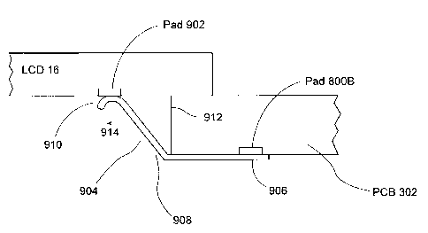
embodiment, display 16 has electrical connection pads 902 on its bottom side
to replace
connector 406 (of Fig. 8).
[0061] In the connection arrangement of this embodiment, to make an electrical
connection between pads 902 and pads 800B, connector 904 is provided. Similar
in
operation and composition to connectors described above, connector 904 is a
set of
isolated, insulated parallel conductors; however, at each end of connector
904, the
conductors are exposed. PCB end 906 of connector 904 is generally shaped to be
flat and
align with pads 800B. PCB end 906 may be electrically and physically secured
to pads
800B using solder, welding techniques or a friction fit arrangement with an
interface
(such as a connector, a clamp, a spring latch or a like mechanism).
[0062] For the embodiment, pads 902 are located on the bottom portion of
display 16 and
device 16 is located about cavity 304 such that pads 902 are located above
cavity 304.
To assist with alignment of connector 904, individual pads 800B and 902 would
be
aligned in parallel, although other alignments can be implemented.
[0063] Middle portion 908 of connector 904 spans between pads 800B and pads
902. As
shown. End portion 910 of connector 904 has a curved tip, curving outwardly
from side
912 of PCB and downwards towards the cavity. When display 16 is not positioned
about
opening 304, connector 904 is in a first position, its pre-connection
position, and is biased
towards side 912 of PCB 302, which is nearest pads 800B. As display 16 is
moved to a
second position, its final location, the bottom side of display 16 engages end
portion 910
and presses down on it. Portion 908 is eased away from its preconnection
position and
moves outward from side 912 and towards connectors 902, generally in the
direction of
arrow 914. When display 16 is in its final position, portion 910 make contact
with pads
-15-
CA 02549892 2006-06-12
902 thereby completing an electrical connection between pads 902 and pads
800B. In
moving from its first position to its second position, as connector 902 is
biased to return
to its first position, the bias imparts an additional force of connector end
910 against pad
902, thereby enhancing the electrical contact between the two components. In
other
S embodiments, other configurations can be made for the relative locations of
pads 902 and
800B and the composition and shape of connector 902. For example, pads 902 may
be
located on an edge of display 16 and connector 904 may be shaped to engage
pads 902.
[0064] Refernng to Figs. 10 and 11, in yet another embodiment, connector 408
is
mounted to a connector on the side of cavity 304. In particular, on wall 1000
of cavity
304, an opening is shown for connector 1002. Therein, an end of connector 406
mates
with connector 1002. As with earlier described embodiments, connector 406 may
be
biased towards wall 1000, in the direction of arrow 1004. In other
embodiments,
connector 1002 is replaced with a set of solder pads, similar to solders pads
800 (Fig. 8),
which are located on wall 1000. For these other embodiments, connector 406
will have
bare ends, similar to bare ends 412 (Fig. 8).
[0065] In other embodiments, as a variation on PCB 302, instead of having a
cavity, like
cavity 302, being completely contained within the borders of a PCB, an
alternative cavity
may be provided as a notch on one side of the PCB. Therein connector 408 may
be fed
through the notch from the top side of the PCB to the bottom side thereof. In
other
embodiments, two separate PCBs may be provided where they are placed in a
spaced
relationship to each other with the spaced relationship defining a gap between
the two
PCBs. Therein, the display may be positioned to span at least partway between
the two
-16-
CA 02549892 2006-06-12
PCBs and then its connector may be positioned to mate with a connector on a
bottom side
of one of the PCBs.
[0066] Referring to Fig. 12, another embodiment is shown where display 16
overhangs
an exterior edge 1200 of PCB 302. Therein, connector 408 extends from the
overhanging
S portion 1202 of display 16 and is shaped to mate with connector 306 on the
bottom
thereof. As is shown in Fig. 8, connector 408 is bent such that it is turned
through an
approximately 90° angle, two 90° angle bends to end up in a
position which is
approximately 180° from its original orientation. In other embodiments,
if connector 408
is positioned to project downwards towards connector 306 and as such, does not
have to
be bent to change its orientation. It will be appreciated that a variation of
this
embodiment may have solder pads, similar to solder pads 800A (Fig. 8) placed
on the
bottom of PCB 302 in lieu of connector 306. Alternatively still, a connector
or a set of
solder pads may be provided on an exterior edge 1200 of PCB 302. Alternatively
still, a
variation on the connector arrangement shown in Fig. 9 may be used.
[0067] It will be appreciated that various PCBs and displays described herein
form an
electronics module which has a slim vertical profile. It will be appreciated
that the term
"connector" may be used to refer to any connector, bridge, solder pad, clamp,
receptacle,
spring-loaded mounting device or generally any means on the PCB which enables
a
connector for a display cable to be secured thereto and provide an electrical
connection to
devices on the PCB.
[0068] It will further be appreciated that cavity 304 shown in Figs. 6-11, as
well as the
overhanging arrangement of the display and the PCB shown in Fig. 12 are
embodiments
wherein the connector for a display is mated to a connector on the PCB. The
PCB
-17-
CA 02549892 2006-06-12
connector is located on a region that is not on the side of the PCB on which
the display is
mounted. The display connector is fed through a cavity or over an open edge of
the PCB
to reach the connector on the PCB.
[0069] Further still, although the embodiments have been described in terms of
a display
S with a connector being connected to the PCB and a connection system
therefor, in other
embodiments, other electronic devices, not necessarily incorporating a
display, but
having a similar connector to those described herein may be used. Such
electronic
devices may include a daughterboard, a microprocessor, memory devices and
electro-
mechanical devices, such as relays.
[0070] The present invention is defined by the claims appended hereto, with
the
foregoing description being merely illustrative of a preferred embodiment of
the
invention. Those of ordinary skill may envisage certain modifications to the
foregoing
embodiments which, although not explicitly discussed herein, do not depart
from the
scope of the invention, as defined by the appended claims.
-18-