Note: Descriptions are shown in the official language in which they were submitted.
CA 02550308 2006-06-16
WO 2005/083804 PCT/IB2004/000201
1
Light Emitting Diode with Integral Heat Dissipation Means
The following invention disclosure is generally concerned with the art of
semiconductor electronics packaging and in particular with forming a thermal
s conductive path integrally with device packaging.
Light emitting diodes are presently made in huge quantities. Generally
speaking, they are very standard in their construct and form. As such, optical
engineers enjoy buying them in bulk and configuring devices and systems from
these standardized packages. However, limitations associated with standard
to designs prevent use of LEDs in some high performance arrangements. For
example, in high brightness applications, several LEDs may be ganged together
to
produce a bright light. This is an inferior solution and one not useful in
certain
systems. A preferred solution may be to drive the LED at a high current to
produce
more light. However, this is not possible because standard LED packages trap
is heat and self destruct when too much current is applied. An LED package
generally is comprised of a hard polycarbonate material which completely
surrounds the semiconductor. When excess heat is trapped, the polycarbonate.
expands and tends to break. Further, the heat tends to cause junction
breakdown
in the semiconductor as well. Heat is a light emitting diode's worst enemy.
ao Thus, skilled practitioners of the art have tried to couple heat away from
LEDs to improve their performance. In particular, heat sink arrangements have
been introduced to carry heat away from the diodes. These heat sinks are
sometimes provided with heat coupling suitable for standard LED packages. In
example, the polycarbonate material may be in intimate contact with a heat
sink.
zs While these arrangements serve their purpose to some extent, they are
limited
because common LED packages are not arranged to cooperate with heat removal
mechanisms.
~O~I~If~RRA'~ION CONY
CA 02550308 2006-06-16
WO 2005/083804 PCT/IB2004/000201
2
While considerable efforts in the material sciences are made to improve the
efficiency of semiconductor diode junctions used in LEDs, these improvements
come slowly and with fractional gains at large expense. The chemistry and
physics
of diode junctions changes slowly in time. Most notably in recent
developments,
s high brightness blue colored chips are becoming more readily available.
Diodes
which emit blue colored light are difficult to produce because blue light is
comprised of higher energy photons which are not easily produced in normal
band
gap junctions. The 'gap' between bands of allowed energies must be quite large
to
form a high energy blue photon. To form a large gap, specialized materials and
to dopants are used in the semiconductor growth and doping. Although these
materials will produce blue photons, they do so with less efficiency than
materials
used to produce other colors. More of the input electrical energy is converted
to
heat than to blue light. This is problematic as the heat is lost as waste. It
is
desirable that one should have the highest possible quantum efficiency to
reduce
is this loss.
Improving the quantum efficiency of the junction is not the only way to
realize high output from a diode. Where waste is not of significant
consequence,
one might simply increase the current to produce a greater flux of light
output.
However, this approach is left with the problem of heat accumulation. Heat
ao produced at the diode junction tends to become excessive and damage the
diode
as well as the package components. LEDs are typically encased in a hard
polycarbonate material which is susceptible to cracking as it becomes brittle
in
heat.
A diode will roughly produce light in proportion to the amount of current
as which is forced through its junction. As one increases the applied current,
the
junction produces more light. This is true, with a very real limitation. As
the current
is increased, the heat produced at the junction is also increased. That heat,
when
it becomes excessive, tends to destroy the diode. The diode will self destruct
and
cease to function as the heat damages the physical structure of the
CA 02550308 2006-06-16
WO 2005/083804 PCT/IB2004/000201
3
semiconductor. Accordingly, common diodes are rated to operate normally at
about 20 milliamps. They will continue to produce greater light outputs beyond
20
milliamps with a lifetime penalty. After a significant current is applied
beyond
twenty milliamps, the device will break and become forever damaged. A primary
s reason the device breaks is due to heat in the junction. If heat can be
drawn away
from the junction at a rate faster than it is produced there, then damage to
the
junction will not occur. Thus, one can increase the current without limit so
long as
the corresponding heat produced as a result can be drawn from the junction at
a
rate greater than which it is produced.
to A common LED is made with metallic leads fashioned as two electrical
conductors, i.e. an anode and a cathode lead to provide an electrical contact
with
the semiconductor materials. An assembly is arranged and a polycarbonate
bonding material is applied to seal elements together whereby the
polycarbonate
totally encases the diode, the electrodes among other elements. Typically, the
is metallic leads also provide mechanical and optical services in the overall
structure
as well. As the metal leads are rigid and strong, LEDs are generally mounted,
for
example into a circuit board, via their electrical leads which protrude from
the
bottom of the polycarbonate cover which typically includes a lens in its top
surface.
The two electrodes provide an electrical path to the semiconductor device
ao which is best set into a mirror or reflective conic section element. The
reflector is
generally formed into the metallic lead. A thin wire may be connected from a
first
electrode to a top surface of the diode. This assembly and arrangement is
placed
into a mold of polycarbonate material in a liquid state before being
polymerized or
subject to other curing. The cover may be formed as a very hard plastic having
a
25 lens thereon its top surface. When current is forced through the
electrodes, light is
produced in the junction and reflects from the conic reflector and passes to
the
lens in the plastic cover. Some of the heat generated at the diode passes down
the electrical lead as it is metal and an excellent thermal conductor.
Although
some heat passes to the opposing lead via the thin wire, this thermal path is
CA 02550308 2006-06-16
WO 2005/083804 PCT/IB2004/000201
4
limited because the gauge of the wire is generally quite small. Some heat also
passes via the polycarbonate cover to the surrounding atmosphere. This is also
severely limited because polycarbonate materials do not conduct heat
efficiently.
When current is increased to produce more light, the device can not draw heat
from the junction at a rate sufficient to keep the operating temperature below
a
damage threshold. Thus, the device will overheat and die. An improved thermal
dissipation mechanism would allow a greater quantity of heat to be removed
from
the device and thus allow a higher current and brighter device.
Inventor Flannagan teaches in US patent 4,394,600 a matrix arrangement
to of light emitting diodes with a common heat carrying plane with interesting
thermal
properties. Similarly, Temple et al, present their inventions as US patent
4,905,075
and suggest a semiconductor package formed in view of heating considerations.
Itoh et al also present LED arrays with thermal conductor elements in US
5,113,232. US patent 5,311,060 also teaches of a heat sink arrangement
is incorporated with a semiconductor package.
Hochstein presents LED arrays with special thermal configurations in his
US patents numbered 5,785,418 and 6,045,240. Sheridan et al teach a pad
including a heat sink and thermal insulation area which relates to electronic
devices. In disclosures entitled "Laser Diode Package with Heat Sink" and
ao "Process for Manufacturing a Laser Diode Having a Heat Sink" Marshall et al
show
use of well designed semiconductor packages to improve heat problems. In
addition, the same inventors include US patent 5,985,684 as a separate
invention.
Stephens et al teach similar special arrangements in both US patents 5,913,108
and 6,310,900. These inventors, among others, recognize the benefits of
removing
2s heat in a semiconductor device to improve performance.
While the systems and inventions of the art are designed to achieve
particular goals and objectives, some of those being no less than remarkable,
these inventions have limitations which prevent their use in new ways now
CA 02550308 2006-06-16
WO 2005/083804 PCT/IB2004/000201
possible. These inventions of the art are not used and cannot be used to
realize
the advantages and objectives of the present invention.
Comes now, Abromov, Vladimir; Agafonov, Dimitry; Shishov, Alexander;
and Scherbakov, Nikolai with inventions of light emitting diodes including
devices
s having specialized means of drawing heat away from critical regions. It is a
primary function of these devices to provide high intens ity outputs while
preserving lifetime. It is a contrast to prior art methods and devices that
these
systems do not suffer from the normal problems associated with over- heating
when being driven at high current levels. A fundamental difference between
to devices of these inventions and those of the art can be found when
considering its
special construction relating to a package with an integrated heat conductive
path.
More particularly, an element of high thermal conductivity, a 'thermal
conductor' is
integrated as part of an LED package design. The thermal conductor is arranged
to provide excellent heat coupling directly with the semiconductor chip; in
some
is cases providing both electrical and thermal contact. The thermal conductor
is also
fashioned whereby heat drawn from the semiconductor is further passed into a
heat sink system. Thermal conductors are arranged to cooperate with the entire
LED package and components thereof. For example, a thermal conductor may
serve as an electrical conductor as well. A thermal conductor may also be
2o arranged as an optical reflective element.
It is a primary object of these inventions to provide light emitting diodes
with
improved packaging.
It is an object of these inventions to provide light emitting diodes with
improved packaging for high current high brightness operation. It is a further
object
25 to provide a thermal conductive path leading away from a semiconductor
diode
junction.
A better understanding can be had with reference to detailed description of
preferred embodiments and with reference to appended drawings. Embodiments
presented are particular ways to realize these inventions and are not
inclusive of
CA 02550308 2006-06-16
WO 2005/083804 PCT/IB2004/000201
6
all ways possible. Therefore, there may exist embodiments that do not deviate
from the spirit and scope of this disclosure as set forth by the claims, but
do not
appear here as specific examples. It will be appreciated that a great
plurality of
alternative versions are possible.
These and other features, aspects, and advantages of the present invention
will become better understood with regard to the following description,
appended
claims and drawings where:
Figure 1 is a cross sectional drawing of a first version;
Figure 2 is an expanded view of Figure 1 with added detail;
1o Figure 3 is a similar cross sectional drawing of another version;
Figure 4 illustrates in cross section an LED package arranged with a special
thermal conductor;
Figure 5 shows a version of a thermal conductor with an optical element
formed therein;
is Figure 6 shows a thermal conductor having a special termination end.
In accordance with each of the preferred embodiments of these invention,
there is provided high current, high brightness light emitting diodes having
an
integral thermal conduction path. It will be appreciated that each of the
embodiments described include unique apparatus and that the apparatus of one
2o preferred embodiment may be different than the apparatus of another
embodiment.
For purposes of this disclosure, an LED sometimes includes a light emitting
semiconductor diode and the package into which it is arranged. A 'support
package' may include electrical elements, optical elements, and thermal
elements
2s among others. Thus, the packaging of a semiconductor chip to produce a
light
source is considered part of the entire device sometimes referred to as an
'LED'.
Accordingly, an LED is more precisely a device comprised of two major
systems. LEDs are made of a semiconductor diode element in cooperation with a
package system. The 'diode' is a special semiconductor device of two material
CA 02550308 2006-06-16
WO 2005/083804 PCT/IB2004/000201
7
types arranged to form a special junction region having light emitting
properties.
The 'package' contains electrical leads, mounting support, optical tensing,
and
thermal conductors. Altho ugh, the LED acronym only suggests the 'diode', it
is
affirmed here that 'LED' also is intended to include the packaging for
purposes of
s this disclosure. In devices of these inventions, mechanisms are provided to
draw
he at away from the diode junction at an exceptional rate. Although such means
can be provided in a great plurality of ways, one will appreciate certain
features
unique to the arrangements first taught here.
Preferred versions of these inventions have a thermal conductor element
to included integrally with the device package. In particular, an element
having
rotational symmetry or axial symmetry forms a platform onto which a
semiconductor or semiconductors may be placed into intimate thermal contact.
Further, the thermal conductor is integrated with a base element which
supports
other system components including a cover and electrical leads for example.
15 Figure 1 illustrates some major components of an LED of these inventions
including a thermal conductor. A hard plastic cover element 1 may be molded
into
a special shape including a lens at its upper surface. A base member 2 forms
support upon which the cover and other elements are coupled. In particular,
the
cover may be pushed tightly onto the base to form an enclosed cavity between
the
2o base and an interior surface of the cover as it is placed onto the base
member.
The base may further support passage of electrical conductor or'lead' 3 by way
of
holes bored there through.
Sometimes these holes in the base substrate are referred to as 'vias'. To
prevent electrical conduction from the lead to the base which may be metallic,
a
Zs special insulator material lines the hole in the base. This insulator 4 may
be
formed of a glass, ceramic or rubber material for example. An important
element of
the package includes a thermal conductor 5. This thermal conductor is
intimately
and thermally connected directly to the semiconductor chip 6 whereby heat is
encouraged to easily passes away from the diode junction into the thermal
CA 02550308 2006-06-16
WO 2005/083804 PCT/IB2004/000201
g
conductor. Heat may be drawn toward the opposite end of the thermal conductor
where it may leave. As shown in the diagram, the semiconductor may sit
symmetrically within a recess formed in the base in the shape of a conic
section 7.
Light emitted from the chip leaves the semiconductor and falls incident upon
the
s conic surfaces which may be polished. The light is then reflected upward
into the
cover element and away from the thermal conductor. The thermal conductor may
also provide electrical contact to the bottom side of the semiconductor. This
electroconductivity may be extended to the base member. As some preferred
versions include bases made from materials which are electrically conductive,
io such as steel, electrical contact from the bottom side of the semiconductor
may
continue through the thermal conductor further through the base and finally
into a
common electrical lead 8. The cover element includes a skirt portion 9 which
is
configured to engage the base with precision. The cover skirt may provide
alignment function, as well as mechanical holding means.
is In certain preferred versions, a soft and flexible gel material fills the
cavity
between the cover and the base. As mentioned above, polycarbonate material
when subject to heat, tends to fracture. Thus, by placing a gel between the
cover
and the base, a flexible buffer prevents damage due to uneven expansion of
rigid
members. The gel further enhances the function of the thermal conductor as it
2o provides a more complete heat circuit from the top and sides of the
semiconductor
chip to the base and directly to the thermal conductor.
Figure 2 is an expanded view of Figure 1 to illustrate further detail with
regard to gel element which is part of the package. The top and sides of the
semiconductor are thermally coupled to the thermal conductor because the gel
is
Zs also a material having appreciably high thermal conductivity; far higher
than air
and polycarbonate materials used in other LED packages. This arrangement
provides maximum coupling between the semiconductor 25 and the thermal
conductor 24. With regard to the Figure, the same base shown in Figure 1 with
the
CA 02550308 2006-06-16
WO 2005/083804 PCT/IB2004/000201
9
electrical lead 22 passing there through the base and providing contact with
the
top surface of the semiconductor via a wire bond connection.
The plastic cover 23 is illustrated with only its bottom surface showing as
forming a cavity between the cover and the base. Into this cavity, the gel 26
is
s inserted or applied.
The gel may be applied before setting the cover to the base and that action
can be helpful in assuring the gel forms good and solid contact between the
gel
and other components. The cover tends to push the flexible gel into tiny
cracks
and spaces 27, in particular between the semiconductor sides and the conic
to section reflector, and pressure is applied when the cover is joined with
the base. In
this arrangement, the semiconductor is perfectly surrounded by material having
high thermal conductivity, and a clear thermal path, i.e. through the thermal
conductor, which operates to draw heat away from the semiconductor.
Although most important elements are well illustrated in Figures 1 and 2,
is details of some alternative secondary elements of these LED devices are
important in some versions. For example, LEDs typically have a reflecting
element
to turn light emitted substantially in a horizontal plane, towards the top of
the
device. In common LEDs that reflector is formed as a conic section into either
of
the electrical connectors. It is not necessary nor desirable to form a conic
section
ao reflector into electrical conductor leads in these inventions. Rather, a
reflector may
be formed into the base member as in the previous example, alternatively into
the
thermal conductor, or into the cover element.
Figure 3 is a cross section diagram of another preferred version of these
inventions having a thermal conductor element formed as an integral part of
the
2s device package. This version stands in contrast to the previous in several
ways.
First, this device employs a plurality of semiconductor elements. As such
these
devices consume a greater footprint at the semiconductor - thermal conductor
junction. The space required to accommodate the plurality of chips is large in
comparison to the single chip case. As such, coupling between the reflector is
CA 02550308 2006-06-16
WO 2005/083804 PCT/IB2004/000201
necessarily different. The reflector is improved if it is larger and placed
farther
away from the chips. Accordingly, the second difference in this version is a
reflector built into the cover element at its under surface. To accommodate
independent drive of each of the chips, a corresponding plurality of
electrical leads is led through the base element. With reference to the
drawing
figure, optically transparent cover 31 includes reflector surface 32. This
surface
may be formed into the plastic material from which the cover is comprised and
metalized with a thin coating of reflective material such as chrome. The
thermal
conductor 33 supports a platform onto which the entire plurality of chips
might be
to soldered. In the present case three chips are shown, however, it is fully
anticipated
that any number of chips might be placed there without loss of generality.
Careful
note should be made with regard to the relationship between the height of the
thermal conductor and the position of the undersurface of the cover which
includes
the reflector. The chips must be properly located with respect to the features
of the
i5 undersurface of the cover in order for it to operate properly to
efficiently couple
light into a controlled output beam. The base 34 may be formed in a similar
manner as the previous example and it easily supports a plurality of via
holes, one
each for each electrical conductor. One wire bond for each semiconductor might
be arranged to be in electrical communication with either electrical lead.
Although
ao semiconductor 36 appears without a connection, the cross section drawing
does
not support objects which extend from the page, thus one will appreciate its
existence without it being shown explicitly. If the base provides a common
electrical connection, via the metallic thermal conductor, then each
electrical lead
37 is isolated from the base via insulators 37. Finally the top surface 39 of
the
z5 cover might include a lens formed as a surface relief pattern. This is
sometimes
and commonly known as a Fresnel type lens. As was used in the previous
example, this version also benefits from addition of a gel material between
the
undersurface of the cover and the base/thermal conductor. In this case, the
thermal conductor is in greater contact with the gel but the operation and
service is
CA 02550308 2006-06-16
WO 2005/083804 PCT/IB2004/000201
11
the same or similar. As the undersurface of the cover is quite complex in
shape,
gel material is optimally used there as it forms itself under pressure to any
complex shape.
Figure 4 illustrates yet another version. This variation extends the principle
of having a cover 41 with a complex curved underside. The LED package includes
a base 42 of steel material and a thermal conductor 43 of copper material.
Electrical lead 44 passes through via lined with insulative material 45 to
provide a
wire bond to the top surface of the semiconductor. Light emitted from the
semiconductor falls incident on lens 46 which is part of the optical elements
to formed into the undersurface of the cover. Space 47 between the base and
the
cover may be filled with gel or may be left with an air buffer. Curved surface
48
forms a parabolic section reflector. The parabola shape may be used where it
is
desirable to couple the light into a highly collimated beam. Ray trace diagram
49
shows that light which glances off the lens falls to the reflector where it
rejoins the
i5 light propagating toward the top surface of the cover. Although a parabolic
shape
is shown for this example, it is done so to illustrate one of possible shapes.
A conic
section similarly provides acceptable function.
Figure 5 illustrates yet another important example. In this case, a conic
section reflector is formed directly into the thermal conductor element as a
recess
2o whereby the recess also has a flat portion or 'floor' to receive the
semiconductor
chip thereon. A semiconductor diode can be placed into the floor of the recess
while the walls of the conic section are made reflective via polishing or
coating. In
this way, the semiconductor forms a strong thermal coupling with respect to
the
thermal conductor while being optically coupled to the top of the cover
element by
zs way of the reflector. Light from the diode is reflected in a direction
towards the top
of the package ; away from the thermal conductor, while at the same time, heat
is
drawn downward away from the semiconductor. One will more fully appreciate
this
arrangement in consideration of drawing Figure 5. A base 51, is provided as a
foundation. Cover element 52 couples thereto said base at the base periphery.
CA 02550308 2006-06-16
WO 2005/083804 PCT/IB2004/000201
12
This coupling may include a mechanical pressure fit or/and adhesive. Thermal
conductor 53 is formed with recess 54 partly in the shape of a conic section
having
a floor. A semiconductor sets in the recess on the floor of the thermal
conductor in
intimate thermal contact therewith. Wire provides electrical contact from the
lead to
s the top surface of the semiconductor chip. Light emitted from the diode
junction
falls incident upon the reflector and is directed toward the lens in the top
surface of
the cover. Heat generated in the diode is drawn quickly away from the junction
and
into the bulk material from which the thermal conductor is formed. Heat
thereafter
is transmitted to a terminal end of the thermal conductor 55. This end may be
put
to into contact with a heat sink of a greater system in agreement with design
considerations. An important aspect of some versions of the cover is further
illustrated here. As it is desirable to provide precise alignment between a
lens and
the reflector/chip the cover and base elements may incorporate an indexing
means 56 to assure the symmetry axes of these elements are colinear. Further,
is special skirt 57 may provide mechanical interlocking between the base and
the
cover whereby it is not easily removed there from. Careful study of the
diagram
proves that the very bottom edge of the skirt does not extend downwardly as
far as
the terminal end of the thermal conductor as indicated in the drawing by
dashed
lines and 'D'. In this way, the thermal conductor is nicely exposed and may be
2o easily coupled to heat sinks arranged with understanding of the designs.
This is
very important in versions where the thermal conductor is to be coupled to an
exterior heat sink. A stand alone LED package can be inserted into a well
designed receptacle such that the thermal conductor portion of the LED package
contacts a heat sink.
25 Excellent thermal contact may be made between the thermal conductor and
a heat sink which is part of an overall system design. In that way, a large
heat
dump may be provided for advanced applications demanding the highest
performance. Another important feature which also relates to alignment is the
placement of an adhesive. Consider the gap in the horizontal plane 58 and the
gap
CA 02550308 2006-06-16
WO 2005/083804 PCT/IB2004/000201
13
in the vertical 59. It is well established in the art that glue placed between
the
cover and the base in the horizon cannot be applied evenly enough to allow
good
alignment; glue tends to gather in one spot or another causing an offset from
the
vertical and rendering the output not well centered. If adhesive is put into
the gap
s 59 rather than between the horizontal surfaces of the base and cover, then
in
conjunction with the indexing means, excellent alignment is achieved.
In versions where the device is to operate without an external heat dump
yet high brightness operation is desired, it becomes necessary to form a heat
transfer mechanism at the terminal end of the thermal conductor away from the
1o chip. In convection systems which rely on air flow to cool the m, a
transfer
mechanism may include a cooling fins set built integrally with the thermal
conductor. A thermal conductor is made part of the LED package and forms
excellent thermal coupling between the semiconductor chip and the air
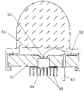
surroundings. Figure 6 illustrates. Base element 61 and cover element 62
having a
i5 lens formed thereon when pressed together form a cavity 63 into which a gel
material is inserted in a similar fashion described in previous examples.
However,
in this embodiment, a thermal conductor 64 is arranged to provide a high flux
thermal path from semiconductor 65 at a first terminal end to its opposite
terminal
end comprised of a cooling fins arrangement 66. Heat is efficiently drawn away
ao from the diode junction and towards the cooling fins and thereafter
transferred into
the surrounding atmosphere. Electrical lead 67 can be fashioned to cooperate
with
the base in the normal way while remaining aside of the cooling fins
arrangement.
Some preferred versions of these thermal conductors includes devices
made of copper or a copper alloy. Copper is a superior material having a very
high
zs thermal conductivity. It is inexpensive and easy to machine. Its lifetime
and
electrical properties cooperate in every way with the properties necessary for
good
LED package design.
Thus it is a preferred material with the note that similar highly conductive
materials may also be suitable.
CA 02550308 2006-06-16
WO 2005/083804 PCT/IB2004/000201
14
One will now fully appreciate how high current, high brightness LEDs may
be formed with a heat management arrangement for high performance. Although
the present invention has been described in considerable detail with clear and
concise language and with reference to certain preferred versions thereof
including the best mode anticipated by the inventor, other versions are
possible.
Therefore, the spirit and scope of the invention should not be limited by the
description of the preferred versions contained therein, but rather by the
claims
appended hereto.