Note: Descriptions are shown in the official language in which they were submitted.
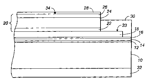
CA 02550368 2009-03-05
IMAGING MEMBER
BACKGROUND
[0001] There is disclosed herein an imaging member used in
electrophotography having a charge transport layer with multiple
concentrations of
charge transport components. More particularly disclosed herein is an imaging
member that has a photogenerating layer and a charge transport layer with one
or
more regions or layers. In each region or layer, the charge transport
components are
molecularly dispersed or dissolved in a polymer binder to form a solid
solution. In
the resulting charge transport layer, the region or layer closest in proximity
to the
photogenerating layer is in contiguous contact therewith and comprises a lower
concentration of charge transport components than a layer spaced from the
photogenerating layer.
[0002] A typical electrophotographic imaging member is imaged by uniformly
depositing an electrostatic charge on an imaging surface of the
electrophotographic
imaging member and then exposing the imaging member to a pattern of activating
electromagnetic radiation, such as light, which selectively dissipates the
charge in
the illuminated areas of the imaging member while leaving behind an
electrostatic
latent image in the non-illuminated areas, This electrostatic latent image may
then
be developed to form a visible image by depositing finely divided
electroscopic
marking toner particles on the imaging member surface. The resulting visible
toner
image can then be transferred to a suitable receiving member, such as paper.
[0003] A number of current electrophotographic imaging members are
multilayered photoreceptors that, in a negative charging system, comprise a
substrate support, an electrically conductive layer, an optional charge
blocking layer,
an optional adhesive layer, a charge generating layer, a charge transport
layer, and
optional protective or overcoating layer(s). The multilayered photoreceptors
can take
several forms, for example, flexible belts, rigid drums, flexible scrolls, and
the like.
Flexible photoreceptor belts may either be seamed or seamless belts. An anti-
curl
layer may be employed on the back side of the flexible substrate support, the
side
opposite to the electrically active layers, to achieve a desired photoreceptor
belt
flatness.
-1-
CA 02550368 2006-06-14
[0004] Although excellent toner images may be obtained with multilayered
belt photoreceptors, a delicate balance in charging image and bias potentials,
and characteristics of toner/developer must be maintained. This places
additional
constraints on photoreceptor manufacturing, and thus, on the manufacturing
yield.
Localized microdefect sites, varying in size of from about 5 to about 200
microns,
can sometimes occur in manufacture, which appear as print defects
(microdefects)
in the final imaged copy. In charged area development, where the charged areas
are printed as dark areas, the sites print out as white spots. These
microdefects are
called microwhite spots. In discharged area development systems, where the
exposed area (discharged area) is printed as dark areas, these sites print out
as
dark spots on a white background. All of these microdefects, which exhibit
inordinately large dark decay, are called charge deficient spots (CDS). Since
the
microdefect sites are fixed in the photoreceptor, the spots are registered
from one
cycle of belt revolution to next. Charge deficient spots have been a serious
problem
for a very long time in many organic photoreceptors, such as multi-layered
benzimidazole perylene photoreceptors where the perylene pigment is dispersed
in
a matrix of a bisphenol Z type polycarbonate film forming binder.
[0005] Whether these localized microdefect or charge deficient spot sites
will show up as print defects in the final document depends, to some degree,
on
the development system utilized and, thus, on the machine design selected. For
example, some of the variables governing the final print quality include the
surface
potential of photoreceptor, the image potential of the photoreceptor,
photoreceptor
to development roller spacing, toner characteristics (such as size, charge,
and the
like), the bias applied to the development rollers and the like. The image
potential
depends on the light level selected for exposure. The defect sites are
discharged,
however, by the dark discharge rather than by the light. The copy quality from
generation to generation is maintained in a machine by continuously adjusting
some
of the parameters with cycling. Thus, defect levels may also change with
cycling.
[0006] Techniques have been developed for the detection of CDS's.
These have largely involved destructive testing, although some contactless
methods have been developed. Additionally, multilayer imaging members have
been developed to block charge injection from the substrate which can give
rise
to CDS's.
-2-
CA 02550368 2009-03-05
[0007] The following applications are mentioned:
[0008] U.S. Patent No. 7,166,397, filed December 23, 2003, entitled
"Imaging Members," by Satchidanand Mishra, et al. discloses a charge
transport layer in which the concentration of a charge transport component
decreases, such as by a decreasing concentration gradient, from the lower
surface to an upper surface in the charge transport layer.
[0009] U.S. Patent No. 7,033,714, filed December 16, 2003, entitled
"Imaging Members," by Anthony M. Horgan, et al. discloses a charge
transport layer of an imaging member which includes a plurality of charge
transport layers coated from solutions of similar or different compositions or
concentrations, wherein the upper or additional transport layer or layers
comprise a lower concentration of charge transport component than the first
(bottom) charge transport layer.
[0010] U.S. Patent No. 6,933,089, filed December 16, 2002, entitled
"Imaging Members," by Anthony M. Horgan et al discloses a dual charge
transport layer in which the top layer comprises a hindered phenol dopant.
[0011] The following patents are mentioned:
[0012] Electrophotographic imaging members having at least two
electrically operative layers including a charge generating layer and a
transport layer comprising a diamine are disclosed in U.S. Patent Nos.
4,265,990, 4,233,384, 4,306,008, 4,299,897, and 4,439,507.
[0013] U.S. Patent No. 5,830,614 relates to a photoreceptor which
comprises a support layer, a charge generating layer, and two charge
transport layers. A first of the charge transport layers consists of charge
transporting polymer comprising a polymer segment in direct linkage to a
charge transporting segment and a second transport layer comprises a
charge transporting polymer as for the first layer, except that it has a lower
weight percent of the charge transporting segment than that of the
-3-
CA 02550368 2006-06-14
first charge transport layer.
[0014] U.S. Patent No. 6,294,300 discloses a photoconductor which includes
a charge transport layer coated over a charge generator layer. A hole
transport
molecule is intentionally added to the charge generator layer preventing
migration of
hole transport molecules from the charge transport layer to the charge
generator
layer.
[0015] U.S. Patent Nos. 5,703,487 and 6,008,653 disclose methods for
detecting CDS's. In the '487 patent, a process for ascertaining the
microdefect
levels of an electrophotographic imaging member includes measuring either the
differential increase in charge over and above the capacitive value or
measuring
reduction in voltage below the capacitive value of a known imaging member and
of a
virgin imaging member and comparing differential increase in charge over and
above the capacitive value or the reduction in voltage below the capacitive
value of
the known imaging member and of the virgin imaging member.
[0016] U.S. Patent No. 6,008,653 discloses a method for detecting surface
potential charge patterns in an electrophotographic imaging member with a
floating
probe scanner. The scanner includes a capacitive probe, which is optically
coupled
to a probe amplifier, and an outer Faraday shield electrode connected to a
bias
voltage amplifier. The probe is maintained adjacent to and spaced from the
imaging
surface to form a parallel plate capacitor with a gas between the probe and
the
imaging surface. A constant voltage charge is applied to the imaging surface
prior to
establishing relative movement of the probe and the imaging surface.
Variations in
surface potential are measured with the probe and compensated for variations
in
distance between the probe and the imaging surface. The compensated voltage
values are compared to a baseline voltage value to detect charge patterns in
the
electrophotographic imaging member
[0017] U.S. Patent Nos. 5,591,554; 5,576,130; and 5,571,649 disclose
methods for preventing charge injection from substrates which give rise to
CDS's.
These patents disclose an electrophotographic imaging member including a
support substrate having a two layered electrically conductive ground plane
layer
comprising a layer comprising zirconium over a layer comprising titanium, a
hole
blocking layer, and an adhesive layer. The adhesive layer of the '554 patent
includes
a copolyester film forming resin, and the member further includes an
intermediate
layer comprising a carbazole polymer, a charge generation layer comprising a
-4-
CA 02550368 2006-06-14
perylene or a phthalocyanine, and a hole transport layer, which is
substantially
non-absorbing in the spectral region at which the charge generation layer
generates and injects photogenerated holes. The adhesive layer of the '130
patent comprises a thermoplastic polyurethane film forming resin. The adhesive
layer of the '649 patent comprises a polymer blend comprising a carbazole
polymer and a film forming thermoplastic resin in contiguous contact with a
hole
blocking layer.
BRIEF DESCRIPTION
[0018] Aspects of the exemplary embodiment relate to an imaging member
and a method of formation. In one aspect, the imaging member includes a
charge generating layer and a charge transport layer. The charge transport
layer
includes a first surface in contact with the charge generating layer and a
second
surface. The charge transport layer includes a film forming polymer binder and
a
charge transport component dispersed therein. The concentration of the charge
transport component in the charge transport layer is at a peak in a region of
the
charge transport intermediate the first and second surfaces of the charge
transport layer.
[0019] In another aspect, an imaging member includes an optional substrate,
a source of charge, and a charge transport layer which receives charge from
the
source. The charge transport layer includes a film forming polymer binder and
a
charge transport component dispersed therein. The charge transport layer
includes
a first region and a second region. The second region is spaced from the
source of
charge by the first region. The first region has a lower charge mobility than
the
second region whereby charge deficient spots are reduced as compared with an
imaging member formed without the first region.
[0020] In another aspect, a method includes forming a charge transport layer
on a charge generating layer, including depositing a first layer on the charge
generating layer. The first layer includes a film forming polymer binder and
optionally a charge transport component dispersed therein. The method further
includes depositing at least one second layer directly or indirectly on the
first layer
such that the at least one second layer is spaced from the charge generating
layer
by the first layer, the at least one second layer comprising a film forming
polymer
-5-
CA 02550368 2009-03-05
binder and a charge transport component dispersed therein, a concentration of
charge transport component in the at least one second layer, upon drying,
being higher than a concentration of charge transport component in the first
layer. A third layer is optionally deposited on the at least one second layer,
the
third layer comprising a film forming polymer binder and optionally a charge
transport component dispersed therein, a concentration of charge transport
component in the third layer, upon drying, being lower than a concentration of
charge transport component in an adjacent second layer An overcoat layer is
optionally deposited over the charge transport layer.
According to another aspect of the present invention, there is
provided an imaging member comprising:
a charge generating layer; and
a charge transport layer comprising a first surface in contact with the
charge generating layer and a second surface, the charge transport layer
comprising a film forming polymer binder and a charge transport component
dispersed therein, wherein the concentration of the charge transport component
in
the charge transport layer is at a peak in a region of the charge transport
layer
intermediate the first and second surfaces of the charge transport layer.
According to another aspect of the present invention, there is provided
an imaging member comprising;
an optional substrate;
a source of charge; and
a charge transport layer which receives charge from the source, the
charge transport layer comprising a film forming polymer binder and a charge
transport component dispersed therein, the charge transport layer comprising a
first region and a second region, the second region being spaced from the
source of charge by the first region, the first region having a lower charge
mobility than the second region whereby charge deficient spots are reduced as
compared with an imaging member formed without the first region.
According to a further aspect of the present invention, there is
provided a method comprising:
-6-
CA 02550368 2010-04-01
forming a charge transport layer on a charge generating layer
comprising:
depositing a first layer on the charge generating layer, the first layer
comprising a film forming polymer binder and optionally a charge transport
component dispersed therein;
depositing at least one second layer directly or indirectly on the first
layer such that the at least one second layer is spaced from the charge
generating layer by the first layer, the at least one second layer comprising
a
film forming polymer binder and a charge transport component dispersed
therein, a concentration of charge transport component in the at least one
second layer, upon drying, being higher than a concentration of charge
transport
component in the first layer;
optionally depositing a third layer on the at least one second layer, the
third layer comprising a film forming polymer binder and optionally a charge
transport component dispersed therein, a concentration of charge transport
component in the third layer, upon drying, being lower than a concentration of
charge transport component in an adjacent second layer; and
optionally depositing an overcoat layer over the charge transport layer.
According to another aspect of the present invention, there is provided
a method comprising:
forming a charge transport layer on a charge generating layer
comprising:
depositing a first layer on the charge generating layer, the first layer
comprising a solvent, a film forming polymer binder and optionally a charge
transport component dispersed therein;
prior to complete drying of the first layer, depositing at least one
second layer directly or indirectly on the first layer such that the at least
one
second layer is spaced from the charge generating layer by the first layer,
the at
least one second layer comprising a film forming polymer binder and a charge
transport component dispersed therein, a concentration of charge transport
component in the at least one second layer, upon drying, being higher than a
concentration of charge transport component in the first layer, the first
layer,
when deposited, being substantially free of charge transport components and
wherein the transport component diffuses from the second layer into the first
-6a-
CA 02550368 2010-04-01
layer prior to complete drying of the first layer;
optionally depositing a third layer on the at least one second layer, the
third layer comprising a film forming polymer binder and optionally a charge
transport component dispersed therein, a concentration of charge transport
component in the third layer, upon drying, being lower than a concentration of
charge transport component in an adjacent second layer; and
optionally depositing an overcoat layer over the charge transport layer.
According to a further aspect of the present invention, there is
provided an imaging member comprising:
a charge generating layer; and
a charge transport layer comprising a first surface in contact with the
charge generating layer and a second surface, the charge transport layer
comprising a film forming polymer binder and a charge transport component
dispersed therein, wherein the concentration of the charge transport component
in
the charge transport layer progressively increases from a lower region closest
in proximity to the charge generation layer and decreases toward an upper
region of the charge transport layer adjacent said second surface.
According to another aspect of the present invention, there is provided
a method comprising:
forming a charge transport layer on a charge generating layer
comprising:
depositing a first layer on the charge generating layer, the first layer
comprising a film forming polymer binder and optionally a charge transport
component dispersed therein;
depositing at least one second layer directly or indirectly on the first
layer such that the at least one second layer is spaced from the charge
generating layer by the first layer, the at least one second layer comprising
a film
forming polymer binder and a charge transport component dispersed therein, a
concentration of charge transport component in the at least one second layer,
upon drying, being higher than a concentration of charge transport component
in
the first layer;
optionally depositing a third layer on the at least one second layer, the
third layer comprising a film forming polymer binder and optionally a charge
transport component dispersed therein, a concentration of charge transport
-6b-
CA 02550368 2010-04-01
component in the third layer, upon drying, being lower than a concentration of
charge transport component in an adjacent second layer; and
optionally depositing an overcoat layer over the charge transport layer,
wherein the first layer further includes a solvent and wherein the
method comprises depositing at least one second layer prior to complete
drying of the first layer.
BRIEF DESCRIPTION OF THE DRAWINGS
[0021] FIGURE 1 is a schematic cross sectional view of an exemplary
imaging member according to a first embodiment;
[0022] FIGURE 2 is a schematic cross sectional view of upper layers of
an exemplary imaging member according to a second embodiment;
[0023] FIGURE 3 shows the concentration of charge transport
component through layer 20 of FIGURE 2;
[0024] FIGURE 4 is a schematic illustration of a slotted dye in process of
forming sub-layers of a charge transport layer of an exemplary imaging member;
and
[0025] FIGURE 5 is a bar graph illustrating the effects of charge
transport component concentration on CDS's in a multilayer photoreceptor.
DETAILED DESCRIPTION
[0026] Aspects of the exemplary embodiments disclosed herein relate to
an imaging member, to a method of formation of an imaging member, and to a
method of use of such an imaging member. Although the embodiments disclosed
herein are applicable to electrophotographic imaging members in flexible belt
configuration and rigid drum form, for reason of simplicity, the discussions
below
are focused upon electrophotographic imaging members in flexible belt designs.
[0027] In aspects of the exemplary embodiment disclosed herein, there is
provided an imaging member comprising a photogenerating (charge generating)
layer with a charge transport layer disposed thereon. The charge transport
layer
has a lower surface which is in contiguous contact with the charge generating
layer, and an upper surface. Additionally, the charge transport layer
comprises a
film forming
-6c-
CA 02550368 2009-03-05
binder and a charge transport component, such as hole transport molecules,
molecularly dispersed or dissolved therein to form a solid solution. A first
layer of
the charge generating layer closest in proximity to the charge generating
layer has a
lower concentration of charge transport component than a second layer spaced
from the charge generating layer. The concentration of the charge transport
component in the charge transport layer may increase stepwise, or gradually,
as
for example, by an increasing concentration gradient, away from the lower
surface toward the upper surface. The concentration of the charge transport
component may progressively increase from the region closest in proximity to
the
photogenerating layer and then may decrease toward the upper region of the
charge transport layer. While the particular reference is made to the charge
transport layer as comprising two or more layers of different concentration of
charge transport component, it is to be appreciated that these layers need not
be discrete layers but may comprise generally parallel regions of the charge
transport layer having different concentrations of charge transport component.
[0028] In aspects disclosed herein, the solid solution charge transport layer
may have multiple regions of different concentrations of charge transport
component. The charge transport layer may comprise a solid solution of
different
concentrations of charge transport components, film forming polymer
binders/resins and other compounds to form two or more regions.
[0029] In one aspect, the charge transport layer comprises different regions
or layers of a solid solution of a film forming polymer binder containing
different
concentrations of charge transport component(s) wherein the layer of the
largest
concentration of charge transport components is spaced from the bottom surface
of
the charge transport layer and lower concentrations of charge transport
components
are at the top and bottom surfaces of the charge transport layer.
[0030] In a further embodiment, the charge transport layer can comprise
multiple charge transport layers consisting of a first or bottom charge
transport
layer comprising a solid solution of a film forming polymer binder and a
charge
transport component, and thereover and in contact with the first layer, a
second
solid solution charge transport layer or layers, spaced from the
photogenerating
layer by the first layer, the second layer having a higher concentration of
charge
transport component than the first layer and optionally one or more additional
solid solution charge transport layers. The second layer and subsequent
-7-
CA 02550368 2006-06-14
additional charge transport layers each can consist of same or different film
forming polymer binder and same or different charge transport component as
that of the first charge transport layer. However, in the additional layers,
the
content of charge transport component is reduced in a stepwise, or graduated,
concentration gradient from the second layer toward the top or uppermost
layer.
The additional charge transport layers can comprise from 1 to about 15 layers
and, more specifically, from I to about 5 layers.
[0031] It has been found that the charge injection from a source such as the
photogenerating layer, into the charge transport layer is influenced by the
number
(concentration) of charge transport molecules in the vicinity. By providing a
layer
which suppresses the migration rate of charge from the charge generating layer
into the charge transport layer, CDS spots in images generated by the imaging
member can be significantly reduced. Both types of CDS spots can be reduced-
discharge development spots, which appear as microblack spots on white
backgrounds, and charger development spots, which appear as microwhite spots
on dark backgrounds, can be suppressed by lowering the concentration of
the charge transport component in the layer adjacent to the charge
generation layer. The mobility of the injected charge is also suppressed
as a result of the lower concentration of charge transport component.
Accordingly, the provision of a second layer which provides a higher charge
mobility,
for example, by incorporating a higher concentration of charge transport
component, spaced from the charge generation layer, facilitates movement of
the
charge through the charge transport layer overall. Charge mobility can be
expressed in terms of average velocity of the charge passing through a unit
area
per unit field of the imaging member.
[0032] The additional charge transport layers in the charge transport layer
may also contain a stabilizing antioxidant such as a hindered phenol. Such a
phenol is present in the top most layer of the charge transport layer in a
reverse concentration gradient to that of the charge transport component. For
example, while the concentration of the charge transport component increases
from the first or bottom layer (or the layer in closest proximity to the
photogenerating layer) and decreases again toward the top layer in the overall
charge transport layer, the concentration of the hindered phenol increases
near
the top surface of the charge transport layer and decreases away from it.
-8-
CA 02550368 2006-06-14
Furthermore, in order to achieve enhanced wear resistance results, the top or
uppermost layer or region of the charge transport layer may further include
particles
dispersions of silica, PTFE, and wax polyethylene for effective lubrication
and
wear life extension or be provided with an overcoat,
[0033] Advantages associated with the imaging members of the present
exemplary embodiment include for example, a reduction in charge deficient
spots
(CDS) in images generated with the imaging member. Additional advantages may
include the avoidance suppression of early onset of charge transport layer
cracking.
Such cracking or micro-cracking can be initiated by the interaction with
effluent of
chemical compounds, such as exposure to volatile organic compounds, like
solvents, selected for the preparation of the members and corona emissions
from
machine charging devices. Such cracking can lead to copy print out defects and
also may adversely affect functional characteristics of the imaging member.
[0034] Processes of imaging, especially xerographic imaging and printing,
including digital printing, are also encompassed by the present disclosure.
More
specifically, the layered photoconductive imaging members of the present
embodiment can be selected for a number of different known imaging and
printing
processes including, for example, electrophotographic imaging processes,
especially xerographic imaging and printing processes wherein charged latent
images are rendered visible with toner compositions of an appropriate charge
polarity. Moreover, the imaging members disclosed are useful in color
xerographic
applications, particularly high-speed color copying and printing processes and
which
members are in embodiments sensitive in the wavelength region of, for example,
from about 500 to about 900 nanometers, and in particular from about 650 to
about
850 nanometers, thus diode lasers can be selected as the light source.
[0035] An exemplary embodiment of the multilayered electrophotographic
imaging member of flexible belt configuration is illustrated in FIGURE 1. The
exemplary imaging member includes an optional support substrate 10 having an
optional conductive surface layer or layers 12,, an optional hole blocking
layer 14,
an optional adhesive layer 16, a charge generating layer 18, a charge
transport layer
20 having two or more layers or sub-layers, optionally consisting of at least
a first
charge transport layer 22, a second charge transport layer 24, and a third
transport
layer 26, and optionally one or more overcoat and/or protective layer(s) 28.
Other
layers of the imaging member may include, for example, an optional ground
strip
-9-
CA 02550368 2009-03-05
layer 30, applied to one edge of the imaging member to promote electrical
continuity
with the conductive layer 12 through the hole blocking layer 14. An anti-curl
back
coating layer 32 may be formed on the backside of the flexible support
substrate.
The layers 14, 16, 16, 18, 22, 24, 26, 28 may be separately and sequentially
deposited on the substrate 10 as solutions comprising a solvent, with each
layer
being dried before deposition of the next. Alternatively or additionally, one
or more of
the layers 24, 26, 28 is applied prior to drying of the previous layer such
that partial
mixing at the boundaries of adjacent layers and/or leaching diffusion of one
or more
components from one layer into the adjacent layer (s) can occur.
[0036] In the illustrated embodiment, layer 20 has a lower surface 33 which is
in
direct contact with the upper surface of the charge generating layer 18 and an
upper
surface 34 which may be the exposed surface of the imaging member if no
overcoat
layer 28 is employed or, where an overcoat layer 28 or layer is used, the
upper
surface 34 is in direct contact with the overcoat layer 28.
[0037] The photoreceptor support substrate 10 may be opaque or substantially
transparent, and may comprise any suitable organic or inorganic material
having the
requisite mechanical properties. The entire substrate can comprise the same
material as that in the electrically conductive surface, or the electrically
conductive
surface can be merely a coating on the substrate. Any suitable electrically
conductive material can be employed. Typical electrically conductive materials
include copper, brass, nickel, zinc, chromium, stainless steel, conductive
plastics
and rubbers, aluminum, semitransparent aluminum, steel, cadmium, silver, gold,
zirconium, niobium, tantalum, vanadium, hafnium, titanium, nickel, chromium,
tungsten, molybdenum, paper rendered conductive by the inclusion of a suitable
material therein or through conditioning in a humid atmosphere to ensure the
presence of sufficient water content to render the material conductive,
indium, tin,
metal oxides, including tin oxide and indium tin oxide, and the like.
[0038] The substrate 10 can also be formulated entirely of an electrically
conductive material, or it can be an insulating material including inorganic
or organic
polymeric materials, such as, MYLARTM, a commercially available biaxially
oriented
polyethylene terephthalate from DuPont, MYLARTM with a coated conductive
titanium surface, otherwise a layer of an organic or inorganic material having
a
semiconductive surface layer, such as indium tin oxide, aluminum, titanium,
and the
-10-
CA 02550368 2006-06-14
like, or exclusively be made up of a conductive material such as, aluminum,
chromium, nickel, brass, other metals and the like. The thickness of the
support
substrate depends on numerous factors, including mechanical performance and
economic considerations.
[0039] The substrate 10 may be flexible, being seamed or seamless for
flexible photoreceptor belt fabrication or it can be rigid for use as an
imaging
member for plate design applications. The substrate may have a number of
many different configurations, such as, for example, a plate, a drum, a
scroll, an
endless flexible belt, and the like. In one embodiment, the substrate is in
the
form of a seamed flexible belt.
[0040] The thickness of the substrate 10 depends on numerous factors,
including flexibility, mechanical performance, and economic considerations.
The
thickness of the support substrate 10 may range from about 50 micrometers to
about 3,000 micrometers; and in embodiments of flexible photoreceptor belt
preparation, the thickness of substrate 10 is from about 50 micrometers to
about
200 micrometers for optimum flexibility and to effect minimum induced
photoreceptor surface bending stress when a photoreceptor belt is cycled
around
small diameter rollers in a machine belt support module, for example, 19
millimeter
diameter rollers. The surface of the support substrate is cleaned prior to
coating to
promote greater adhesion of the deposited coating composition.
[0041] An exemplary substrate support 10 is not soluble in any of the
solvents used in each coating layer solution, is optically transparent, and is
thermally stable up to a high temperature of about 150 C. A typical substrate
support 10 used for imaging member fabrication has a thermal contraction
coefficient ranging from about 1 x 10"5/ C to about 3 x 10⁻⁵/ C and a Young's
Modulus of between about 5 x 10⁵ psi (3.5 x 10⁴ Kg/cm2) and about 7 x 10' psi
(4.9 x
104 Kg/cm2).
[0042] The conductive layer 12 may vary in thickness depending on the
optical transparency and flexibility desired for the electrophotographic
imaging
member. When a photoreceptor flexible belt is desired, the thickness of the
conductive layer 12 on the support substrate 10, for example, a titanium
and/or
zirconium conductive layer produced by a sputtered deposition process,
typically
ranges from about 20 Angstroms to about 750 Angstroms to enable adequate light
-11-
CA 02550368 2006-06-14
transmission for proper back erase, and in embodiments from about 100
Angstroms to about 200 Angstroms for an optimum combination of electrical
conductivity, flexibility, and light transmission. The conductive layer 12 may
be an
electrically conductive metal layer which may be formed, for example, on the
substrate by any suitable coating technique, such as a vacuum depositing or
sputtering technique. Typical metals suitable for use as conductive layer 12
include aluminum, zirconium, niobium, tantalum, vanadium, hafnium, titanium,
nickel, stainless steel, chromium, tungsten, molybdenum, combinations thereof,
and the like. Where the entire substrate is an electrically conductive metal,
the
outer surface thereof can perform the function of an electrically conductive
layer
and a separate electrical conductive layer may be omitted.
[0043] A positive charge (hole) blocking layer 14 may then optionally be
applied to the substrate 10 or to the layer 12, where present. Generally,
electron
blocking layers for positively charged photoreceptors allow the photogenerated
holes in the charge generating layer 18 at the surface of the photoreceptor to
migrate toward the charge (hole) transport layer below and reach the bottom
conductive layer during the electrophotographic imaging processes. Thus, an
electron blocking layer is normally not expected to block holes in positively
charged photoreceptors, such as, photoreceptors coated with a charge
generating
layer over a charge (hole) transport layer. Any suitable hole blocking layer
capable
of forming an effective barrier to holes injection from the adjacent
conductive
layer 12 into the photoconductive or photogenerating layer may be utilized.
The
charge (hole) blocking layer may include polymers, such as, polyvinylbutyral,
epoxy resins, polyesters, polysiloxanes, polyamides, polyurethanes, HEMA,
hydroxypropyl cellulose, polyphosphazine, and the like, or may comprise
nitrogen
containing siloxanes or silanes, nitrogen containing titanium or zirconium
compounds, such as, titanate and zirconate. Hole blocking layers having a
thickness in wide range of from about 50 Angstroms (0.005 micrometers) to
about
micrometers depending on the type of material chosen for use in a
photoreceptor design. Typical hole blocking layer materials include, for
example, trimethoxysilyl propylene diamine, hydrolyzed trimethoxysilyl propyl
ethylene diamine, N-beta-(aminoethyl) gamma-amino-propyl trimethoxy silane,
isopropyl 4-aminobenzene sulfonyl, di(dodecylbenzene sulfonyl) titanate,
isopropyl
di(4-aminobenzoyl)isostearoyl titanate, isopropyl tri(N-
-12-
CA 02550368 2009-03-05
ethylaminoethylamino)titanate, isopropyl trianthranil titanate, isopropyl
tri(N,N-dimethylethy[amino)titanate, titanium-4-amino benzene sulfonate
oxyacetate, titanium 4-aminobenzoate isostearate oxyacetate,
[H2N(CH2)4]CH3Si(OCH3)2, (gammaaminobutyl)-methyl diethoxysilane, and
[H2N(CH2)3]CH33Si(OCH3)2, (gammaaminopropyl)-methyl diethoxysilane, and
combinations thereof, as disclosed in U.S. Patent Nos. 4,338,387, 4,286,033
and 4,291,110. Other suitable charge blocking layer polymer compositions
are also described in U.S. Patent No. 5,244,762. These include vinyl hydroxyl
ester and vinyl hydroxy amide polymers wherein the hydroxyl groups have been
partially modified to benzoate and acetate esters which modified polymers are
then blended with other unmodified vinyl hydroxy ester and amide unmodified
polymers. An example of such a blend is a 30 mole percent benzoate ester of
poly (2-hydroxyethyl methacrylate) blended with the parent polymer poly (2-
hydroxyethyl methacrylate). Still other suitable charge blocking layer polymer
compositions are described in U.S. Patent No. 4,988,597. These include
polymers containing an alkyl acrylamidoglycolate alkyl ether repeat unit. An
example of such an alkyl acrylamidoglycolate alkyl ether containing polymer is
the copolymer poly(methyl acrylamidoglycolate methyl ether-co-2-
hydroxyethyl methacrylate).
[0044] The blocking layer 14 is continuous and may have a thickness of
less than about 10 micrometers because greater thicknesses may lead to
undesirably high residual voltage. In aspects of the exemplary embodiment, a
blocking layer of from about 0.005 micrometers to about 2 micrometers
facilitates charge neutralization after the exposure step and optimum
electrical performance is achieved. The blocking layer may be applied by
any suitable conventional technique, such as, spraying, dip coating, draw
bar coating, gravure coating, silk screening, air knife coating, reverse roll
coating, vacuum deposition, chemical treatment, and the like. For
convenience in obtaining thin layers, the blocking layer may be applied in the
form of a dilute solution, with the solvent being removed after deposition of
the
coating by conventional techniques, such as, by vacuum, heating, and the like.
Generally, a weight ratio of blocking
-13-
CA 02550368 2006-06-14
layer material and solvent of between about 0.05:100 to about 5:100 is
satisfactory for spray coating.
[0045] The optional adhesive layer 16 may be applied to the hole blocking
layer 14. Any suitable adhesive layer may be utilized. One well known adhesive
layer includes a linear saturated copolyester reaction product of four diacids
and
ethylene glycol. This linear saturated copolyester consists of alternating
monomer
units of ethylene glycol and four randomly sequenced diacids in the above
indicated ratio and has a weight average molecular weight of about 70,000. If
desired, the adhesive layer may include a copolyester resin. The adhesive
layer is
applied directly to the hole blocking layer. Thus, the adhesive layer in
embodiments
is in direct contiguous contact with both the underlying hole blocking layer
and the
overlying charge generating layer to enhance adhesion bonding to provide
linkage.
In embodiments, the adhesive layer is continuous.
[0046] Any suitable solvent or solvent mixtures may be employed to form a
coating solution of the polyester. Typical solvents include tetrahydrofuran,
toluene,
methylene chloride, cyclohexanone, and the like, and mixtures thereof. Any
other
suitable and conventional technique may be used to mix and thereafter apply
the
adhesive layer coating mixture to the hole blocking layer. Typical application
techniques include spraying, dip coating, roll coating, wire wound rod
coating, and
the like. Drying of the deposited wet coating may be effected by any suitable
conventional process, such as oven drying, infra red radiation drying, air
drying, and
the like.
[0047] The adhesive layer 16 may have a thickness of from about 0.01
micrometers to about 900 micrometers after drying. In embodiments, the dried
thickness is from about 200 micrometers and about 900 micrometers, although
thicknesses of from about 0.03 micrometers to about 1 micrometer are
satisfactory
for some applications. At thicknesses of less than about 0.01 micrometers, the
adhesion between the charge generating layer and the blocking layer is poor
and
delamination can occur when the photoreceptor belt is transported over small
diameter supports such as rollers and curved skid plates.
[0048] The photogenerating (charge generating) layer 18 may thereafter be
applied to the blocking layer 14 or adhesive layer 16, if one is employed. To
create a
functional charge transport layer, charge transport molecules may be added to
a
-14-
CA 02550368 2009-03-05
polymeric matrix to make it electrically active, since the polymer material is
itself
inherently incapable of supporting the injection of photogenerated holes and
incapable of allowing the transport of these holes through it. Any suitable
charge
generating binder layer 18 including a photogenerating/photoconductive
material,
which may be in the form of particles and dispersed in a film forming binder,
such as
an inactive resin, may be utilized. Examples of photogenerating materials
include,
for example, inorganic photoconductive materials such as amorphous selenium,
trigonal selenium, and selenium alloys selected from the group consisting of
selenium-tellurium, selenium-tellurium-arsenic, selenium arsenide and mixtures
thereof, and organic photoconductive materials including various
phthalocyanine
pigment such as the X-form of metal free phthalocyanine, metal phthalocyanines
such as vanadyl phthalocyanine and copper phthalocyanine, quinacridones,
dibromo anthanthrone pigments, benzimidazole perylene, substituted 2,4-diamino-
triazines, polynuclear aromatic quinones, and the like dispersed in a film
forming
polymeric binder. Selenium, selenium alloy, benzimidazole perylene, and the
like
and mixtures thereof may be formed as a continuous, homogeneous
photogenerating layer. Benzimidazole perylene compositions are well known and
described, for example, in U.S. Patent No. 4,587,189. Multi-photogenerating
layer
compositions may be utilized where a photoconductive layer enhances or reduces
the properties of the photogenerating layer. Other suitable photogenerating
materials known in the art may also be utilized, if desired. The
photogenerating
materials selected should be sensitive to activating radiation having a
wavelength
between about 600 450 and about 700 to 850 nm during the imagewise radiation
exposure step in an electrophotographic imaging process to form an
electrostatic
latent image.
[0049] Any suitable inactive resin materials may be employed in the
photogenerating layer 18, including those described, for example, in U.S.
Patent No.
3,121,006. Typical organic resinous binders include thermoplastic and
thermosetting resins such as one or more of polycarbonates, polyesters,
polyamides, polyurethanes, polystyrenes, polyarylethers, polyarylsulfones,
polybutadienes, polysulfones, polyethersulfones, polyethylenes,
polypropylenes,
polyimides, polymethylpentenes, polyphenylene sulfides, polyvinyl butyral,
polyvinyl acetate, polysiloxanes,
-15-
CA 02550368 2006-06-14
polyacrylates, polyvinyl acetals, polyamides, polyimides, amino resins,
phenylene
oxide resins, terephthalic acid resins, epoxy resins, phenolic resins,
polystyrene and
acrylonitrile copolymers, polyvinylchloride, vinylchloride and vinyl acetate
copolymers, acrylate copolymers, alkyd resins, cellulosic film formers,
poly(amideimide), styrene-butadiene copolymers,
vinylidenechloride/vinylchloride
copolymers, vinylacetate/vinylidene chloride copolymers, styrene-alkyd resins,
and
the like.
[0050] The photogenerating material can be present in the resinous binder
composition in various amounts. Generally, from about 5 percent by volume to
about
90 percent by volume of the photogenerating material is dispersed in about 10
percent by volume to about 95 percent by volume of the resinous binder, and
more
specifically from about 20 percent by volume to about 30 percent by volume of
the
photogenerating material is dispersed in about 70 percent by volume to about
80
percent by volume of the resinous binder composition.
[0051] The photogenerating layer 18 containing the photogenerating
material and the resinous binder material generally ranges in thickness of
from
about 0.1 micrometer to about 5 micrometer for example, from about 0.3
micrometers to about 3 micrometers when dry. The photogenerating layer
thickness is generally related to binder content. Higher binder content
compositions generally employ thicker layers for photogeneration.
[0052] The charge transport layer 20 is thereafter applied over the charge
generating layer 18 and may include any suitable transparent organic polymer
or
non-polymeric material capable of supporting the injection of photogenerated
holes
or electrons from the charge generating layer 18 and capable of allowing the
transport of these holes through the charge transport layer to selectively
discharge
the surface charge on the imaging member surface. In one embodiment, the
charge
transport layer 20 not only serves to transport holes, but also protects the
charge
generating layer 18 from abrasion or chemical attack and may therefore extend
the
service life of the imaging member. The charge transport layer 20 can be a
substantially non-photoconductive material, but one which supports the
injection of
photogenerated holes from the charge generation layer 18. In one embodiment
the
charge transport layer is free or substantially free of photogenerating
materials (e.g.,
layers 22, 24, and 26 each contain less than 1% of the concentration of
-16-
CA 02550368 2006-06-14
photogenerating materials in the charge generating layer 18 and in one
embodiment, less than 0.01 % thereof). The layers or sub-layers 22, 24, 26 of
the
overall charge transport layer 20 are normally transparent in a wavelength
region in
which the electrophotographic imaging member is to be used when exposure is
effected therethrough to ensure that most of the incident radiation is
utilized by the
underlying charge generating layer 18. Each charge transport layer should
exhibit
excellent optical transparency with negligible light absorption and neither
charge
generation nor discharge if any, when exposed to a wavelength of light useful
in
xerography, e.g., 4000 to 9000 Angstroms. In the case when the photoreceptor
is
prepared with the use of a transparent substrate 10 and also a transparent
conductive layer 12, imagewise exposure or erase may be accomplished through
the substrate 10 with all light passing through the back side of the
substrate. In this
case, the materials of the layers or sub-layers 22, 24, and 26 need not
transmit light
in the wavelength region of use if the charge generating layer 18 is
sandwiched
between the substrate and the charge transport layer 20. The charge transport
layer
20 in conjunction with the charge generating layer 18 is an insulator to the
extent
that an electrostatic charge placed on the charge transport layer is not
conducted in
the absence of illumination. The first or bottom charge transport layer 22 and
the
intermediate and top charge transport layers 24, 26 should trap minimal
charges as
the case may be passing through it. Charge transport layer materials are well
known
in the art.
[0053] The charge transport layer 20 may include any suitable charge
transport component or activating compound useful as an additive molecularly
dispersed in an electrically inactive polymeric material to form a solid
solution and
thereby making this material electrically active. The charge transport
component
may be added to a film forming polymeric material which is otherwise incapable
of supporting the injection of photogenerated holes from the generation
material
and incapable of allowing the transport of these holes therethrough. This
converts the electrically inactive polymeric material to a material capable of
supporting the injection of photogenerated holes from the charge generation
layer
18 and capable of allowing the transport of these holes through the charge
transport layer 20 in order to discharge the surface charge on the charge
transport layer. The charge transport component typically comprises small
-17-
CA 02550368 2009-03-05
molecules of an organic compound which cooperate to transport charge
between molecules and ultimately to the surface of the charge transport layer.
[0054] Although the film forming polymer binder used may be different
for different charge transport layers 22, 24, 26 in one embodiment, an
identical
polymer binder is used throughout the charge transport layer 20 which tends
to provide improved interfacial adhesion bonding between the sub-layers 22,
24, 26.
[0055] Any suitable inactive resin binder soluble in methylene chloride,
chlorobenzene, or other suitable solvent may be employed in the charge
transport layer. Exemplary binders include polyesters, polyvinyl butyrals,
polycarbonates, polystyrene, polyvinyl formals, and combinations thereof. The
polymer binder used for the charge transport layers may be, for example,
selected from the group consisting of polycarbonates, polyester, polyarylate,
polyacrylate, polyether, polysulfone, combinations thereof, and the like.
Exemplary polycarbonates include poly(4,4'-isopropylidene diphenyl
carbonate), poly(4,4'-diphenyl-1,1'-cyclohexene carbonate), and combinations
thereof. The molecular weight of the binder can be for example, from about
20,000 to about 1,500,000. One exemplary binder of this type is a MakrolonTM
binder, which is available from Bayer AG and comprises poly(4,4'-
isopropylidene diphenyl) carbonate having a weight average molecular weight
of about 120,000.
[0056] Exemplary charge transport components include those described
in above-mentioned U.S. Patent Nos. 7,033,714; 7,166,397 and 6,933,089,
which may be used singly or in combination for layers 22 and 24. Exemplary
charge transporting components include aromatic diamines, such as aryl
diamines. The charge transport component can comprise an aryl amine selected
from the group consisting of diphenyl diamines, triphenyl amines, terphenyl
diamines, and combinations thereof. Exemplary diphenyl diamines suited for use
as the charge component, singly or in combination, are represented by the
molecular Formula I below:
-18-
CA 02550368 2009-03-05
FORMULA 1
C1 N
wherein each X is independently selected from the group consisting of alkyl,
hydroxy,
and halogen. Typically, the halogen is a chloride. Where X is alkyl, X can
comprise from
1 to about 10 carbon atoms, e.g., from 1 to 5 carbon atoms, such as methyl,
ethyl,
propyl, butyl, and the like. Exemplary aromatic diamines of this type include
N,N'-
diphenyl-N, N'-bis(alkylphenyl)-1,1'-biphenyl-4,4-diamines, such as mTBD,
which has
the formula (N,N'-diphenyl-N,N'-bis[3-methyl phenyl]-[1,1 '-biphenyl]-4,4'-
.diamine);
N,N'-diphenyl-N,N'-bis(chlorophenyl)-1,1'-biphenyl-4,4'-diamine; and N,N'-bis-
(4-
methylphenyl),N,N'-bis(4-ethylphenyl)-1,1'-3,3dimethylbiphenyl)-4,4-diamine
(Ae-16),
and combinations thereof.
[0057] Other layers such as conventional ground strip layer 30 including, for
example, conductive particles dispersed in a film forming binder may be
applied to one
edge of the imaging member to promote electrical continuity with the
conductive layer 12
through the hole blocking layer 14, and adhesive layer 16. Ground strip layer
30 may
include any suitable film forming polymer binder and electrically conductive
particles.
Typical ground strip materials include those enumerated in U.S. Patent No.
4,664,995. The ground strip layer 28 may have a thickness from about 7
micrometers
to. about 42 micrometers, for example, from about 14 micrometers to about 23
micrometers. Optionally, an overcoat layer 26, if desired, may also be
utilized to
provide imaging member surface protection as well as improve resistance to
abrasion
and scratching.
[0058] In one embodiment, the charge transport layer 20 comprises multiple
concentration regions of a binary solid solution comprising a film forming
polymer
binder and a charge transport component comprising one or more aromatic amine
hole
transporting compounds according to Formula I or any other suitable aromatic
amine of
the type disclosed herein. The first layer 22, closest to the charge
generating layer
18, has a lower concentration of charge transport component than layer 24 and
may
comprise, for example, at least about 5 weight percent and may comprise up to
about
-19-
CA 02550368 2009-03-05
40 weight percent of charge transport component, e.g., from about 10 to about
35 wt%.
All charge transport component concentrations are expressed by weight of the
dried
layer, unless otherwise indicated. The second layer 24, spaced from the charge
generation layer by the first layer, has a higher concentration of charge
transport
component than the first layer, such that the mobility of charge in the second
layer is
higher than in the first layer. The second layer 24, may comprise, for
example, at least
about 30 weight percent and may comprise up to about 90 weight percent of
charge
transport component, e.g., from about 35 to about 50 wt%. The concentration of
the
charge transport component in the first layer can be from about 1 % to about
95% of the
concentration of the charge transport component in the second layer, expressed
by
weight. In one embodiment, the charge transport component concentration in the
first
layer is at least about 5% of that of the second layer, in another embodiment,
at least
about 20%, and in yet another embodiment, at least 30%, In one embodiment, the
charge transport component concentration in the first layer is less than about
90% of
that of the second layer, in another embodiment, less than about 80%, and in
yet
another embodiment, about 60% or less of that of the second layer. At low
concentration ratios, the effects of the low concentration of the charge
transport
component in the first layer 22 on the charge mobility can be offset by making
layer 22
of a lower thickness than layer 24.
[0059] The ratio of charge mobility in the second layer 24 to that in the
first layer
can 22 be, for example, from about 5:1 to about 100:1.
[0060] The first layer 22 may be from about 2 to about 15 microns in
thickness.
In one embodiment, the first layer is from about 5 microns to about 15 microns
in
thickness and the second layer total thickness can be from about 10 microns to
about
35 microns in thickness.
[0061] In the illustrated embodiment, the thickness of the first layer 22 is
less
than that of the second layer 24. For example, the ratio of the thickness of
the second
layer 24 to that of the first layer 22 can be, for example, at least about
1.2:1 and in one
embodiment, at least 1,5:1 and in another embodiment, at least about 1.8:1.
The ratio
can be up to about 10:1, or higher. As noted above, the higher ratios are
particularly
suited to cases where the concentration ratio is high.
[0062] Layer 26 is spaced from the charge generating layer 18 by the layers 22
and 24. Layer 24 is thus sandwiched between layers 22 and 26, with layer 26
providing
-20-
CA 02550368 2009-03-05
the upper surface 34 of the charge transport layer 20. Layer 26 may be in
contiguous
contact with layer 24, or where several layers 24 are employed, with the
uppermost layer
24.
[0063] Layer 26 may be similarly formed to layers 22 and 24 in that it
contains a
charge transport component, such as that used for layers 22 and 24, or a
different
charge transport component, which may be any suitable charge transport
component useful as an additive molecularly dispersed in an electrically
inactive
polymeric material to form a solid solution and thereby making this material
electrically active. The third layer 26 has a concentration of the charge
transport
component which can be higher or lower or about the same as the concentration
in the
layer 24. In the exemplary embodiment, the third layer (or region) 26 has a
lower
concentration of the charge transport component than the layer 24. The charge
mobility
in layer 26 may thus be lower than in layer 24. For example, the concentration
of the
charge transport component in the third layer can be from about 1% to about
95% of
the concentration of the charge transport component in the second layer (or
from
about 1% to about 95% of the highest concentration in layer 24, where the
concentration varies in layer 24). In one embodiment the charge transport
component
concentration in the third layer is at least about 5% of that of the second
layer 24, in
another embodiment, at least about 20%, and in yet another embodiment, at
least 30%.
In one embodiment the charge transport component concentration in the third
layer 26
is less than about 90% of that of the second layer, in another embodiment,
less than
about 80%, and in yet another embodiment, about 60% or less of that of the
second
layer. In one embodiment, the concentration of the charge transport component
in
the third layer (or region) 26 is from about 10% to about 80% of the peak
concentration of the charge transport component. The charge transport
component
concentration in the third layer can be approximately the same or somewhat
higher or
lower than that of the first layer, for example, from about 50% to about 300%
of the
concentration in the first layer. The concentration of the charge transport
component in
the charge transport layer 20, in this embodiment, thus increases with
distance from
the charge generation layer 18 and then decreases again towards the upper
surface of
the charge transport layer.
[0064] The thickness of the third layer 26 can be less than the thickness of
the
second layer and can be from about 2 microns to about 10 microns.
[0065] The third layer 26, may comprise, for example, at least about 5 weight
-21-
CA 02550368 2006-06-14
percent and may comprise up to about. 50 weight percent of charge transport
component, e.g., from about 5 to about 45 wt%.
[0066] In one exemplary embodiment, the charge transport layer includes a
layer 22 which comprises 10-35% by weight mTBD, a layer 24 which comprises 40-
60% mTBD and optionally a layer 26 which comprises 5-50% mTBD as the charge
transport component. In this embodiment, layer 22 may be about 10 microns in
thickness layer 24 about 20 microns in thickness and layer 26 about 10 microns
in
thickness. However it is understood that the thickness of the layers 22, 24,
26 can
vary and that layers 22 and 24 can even be equal in thickness. An exemplary
charge
transport layer formed according to FIGURE 1 may have a first layer 22
comprising
about 30% mTBD as the charge transport component and a second layer 24, of
greater thickness than the first layer 22, comprising about 50% mTBD as the
charge
transport component, and a third layer comprising less than 50% mTBD, e.g.,
about
40% or less.
[0067] In another exemplary embodiment, layer 22 comprises 5-10% by
weight mTBD and layer 24 comprises 20-60% mTBD. in this embodiment, layer 22
may be about 8 microns in thickness and layer 24 about 22 microns in
thickness.
[0068] Another exemplary charge transport layer formed according to
FIGURE 1 may have a first layer 22 comprising about 20% mTBD as the charge
transport component, a second layer 24, of greater thickness than the first
layer
22, comprising about 55% mTBD as the charge transport component, and a third
layer 26, of lower thickness than the second layer, comprising about 30% mTBD
as
the charge transport component.
[0069] In another embodiment of an imaging member, illustrated in FIGURE 2,
which can be similarly configured to the embodiment of FIGURE 1, except with
respect to the charge transport layer 20, the concentration of the charge
transport
component increases away from the charge generation layer 18 and reaches a
peak
concentration value intermediate the upper and lower surfaces of the charge
transport layer 20. In this embodiment, the layers 22, 24, 26 are in the form
of
contiguous regions of gradually changing concentration. The concentration
change
may be a continuous increase and then decrease as illustrated in the graph of
concentration vs. depth adjacent the charge transport layer of FIGURE 2, or a
more
-22-
CA 02550368 2006-06-14
stepwise increase and decrease. The concentration can range for example, from
about 2-8% (or whatever level is sufficient to permit at least some charge
migration
from the surface 32 into the charge transport layer) at or adjacent the
surface 32 up
to about 40-90%, e.g., about 50% at the peak 42, and drop to about 2-8% at or
adjacent the surface 34 (or whatever level is sufficient to permit at least
some
charge migration to the surface 34).
[0070] The charge transport layer 20 of FIGURE 2 may be formed by
sequential deposition of multiple sub-layers on the charge generation layer
18. For
example, there may be from three to about 15 sublayers, such as three, five,
six,
eight, or more sub-layers. In one embodiment, the sub-layers are not dried or
are only partially dried prior to application of the subsequent sub-layer. As
a
result, partial mixing occurs at the boundaries between the sub-layers and/or
diffusion of the charge transport component across the boundary between the
sub-layers, and a more gradual variation, rather than step wise variation, in
concentration of the charge transport component is achieved. For example, the
solutions of different concentrations are deposited via slots 50, 52, 54, 56,
58, etc.
in a slotted extrusion die 60, as illustrated in FIGURE 4 to form sub-layers
62, 64,
66, 68, 70, respectively on charge generation layer 18 as the imaging member
moves relative to the die 60 in the direction of arrow D. Slots 50, 52, and
54, are
arranged in a subsequent fashion so that slot 50 carries a solution of low (or
zero) concentration of charge transport component which is extruded directly
over the dried charge generation layer 18, while slots 52 and 54 each extrude
a
solution of increasing charge transport component concentration, which
dispense
each subsequent wet coating sub-layer on top the respective prior wet coating
sub-
layer as the imaging member web stock is moving in the direction of arrow D.
The
slots 56 and 58 extrude a solution of decreasing charge transport component
concentration. Each subsequent sub-layer is applied while the preceding sub-
layer
is in a partially dried state (which may be defined as containing solvent of
not less
than 5 weight percent). This arrangement and process promotes the interfacial
charge transport component diffusion and leads to final convergence of these
layers into a merging, charge transport layer 20, containing an ascending and
then descending charge transport component concentration gradient profile in
the
resulting dried charge transport layer 20 shown in FIGURE 3. The highest
-23-
CA 02550368 2009-03-05
concentration is intermediate the bottom and the top sub-layers 62, 70, such
as in one or
more of sub-layers 64, 66, and 68, which define(s) the intermediate region 24.
Alternatively, the charge transport layer coating application can be
accomplished through
utilizing multiple coating dies that yield a similar result.
[0071] It will be appreciated that while five sub-layers are illustrated in
FIGURE 4,
fewer or more than five sub-layers may be employed. The slots 50, 52, 54, 56,
58, 60
may be spaced to allow partial drying, through solvent evaporation, prior to
application
of the subsequent layer. Alternatively, a heater or heaters may be positioned
adjacent
the sub-layers to assist in drying. Where the lowermost sub-layer 62 is
relatively thin,
such as from about 2 micrometers to about 20 micrometers when dry, e.g., from
about 10 to about 15 micrometers, the concentration of the charge transport
component
in the solution applied may be zero or close to zero (i.e., the first layer,
when deposited,
is substantially free of charge transport components). Charge transport
component
migration from the subsequently applied second sub-layer 64 into this thin
layer 62
provides sufficient charge transport component to permit charge migration
through the
layer 62, once dried. It will be appreciated that in use, the sub-layer 62
contains at least
a minimum concentration of charge transport component sufficient to effect
movement
of charge (holes) through the sub-layer. In a similar way, concentration of
the charge
transport component in the solution applied to form the top sub-layer 70 may
be zero or
close to zero as it is extruded through slot 58, Charge transport component
migration from
the partially-dried, previously-applied sub-layer 68 into the thin layer 70
provides sufficient
charge transport component in sub-layer 70 to permit charge migration through
the sub-
layer 70, once dried. A similar approach may be employed in the embodiment of
FIGURES 1 and 2, where if the lowermost layer 22 is applied as a thin enough
layer, it
can contain little or no charge transport component since migration of the
charge
transport component from layer 24 into the partially dried layer 22 provides
sufficient
charge transport component to permit charge migration through the layer 22,
once
dried.
[0072] The thickness of the first or bottom charge transport sub-layer 62,
when
dried, can be from about 0.5 to about 10 micrometers, e.g., about 3-7
micrometers. The
subsequent sub-layers may have a similar thickness or a greater or lesser
thickness,
depending on the number of sub-layers employed. The overall thickness of the
charge
transport layer 20 can be from about 5
-24-
CA 02550368 2010-04-01
micrometers to about 200 micrometers and is generally from about 10 to about
40 microns and more specifically from 20 to 35 microns.
[0073] If desired, the composition of the top charge transport layer 26 in
each
of the photoreceptors described in the above embodiments may also include, for
example, additions of antioxidants, leveling agents, surfactants, wear
resistant fillers
such as dispersion of polytetrafluoroethylene (PTFE) particles and silica
particles,
light shock resisting or reducing agents, and the like, to impart further
photo-
electrical, mechanical, and copy print-out quality enhancement outcomes,
particularly if no overcoat layer 28 is used.
[0074] CDS's are suppressed by the layer 22 while the lower concentration
of the charge transport component in the top layer 26 near the exposed surface
reduces problems arising from corona effluents and solvents in the surrounding
atmosphere, such as cracking and lateral charge migration (LCM). Charge
transport
components, such as mTBD tend to be oxidized by these effluents. Thus, a lower
concentration in the upper layer 40 mitigates these effects,
[0075] Additional aspects relate to the inclusion in the charge transport
layer
20 of variable amounts of an antioxidant, such as a hindered phenol. Exemplary
hindered phenols include octadecyl-3,5-di-tert-butyl-4-hydroxyhydrociannamate,
available as IrganoxTM 1-1010 from Ciba Specialty Chemicals. The hindered
phenol
may be present at about 10 weight percent based on the concentration of the
charge transport component. The hindered phenol concentration may be is
tailored
to produce a continuum of varying concentration of the antioxidant in reversal
to that
of the charge transport component for improved electrical stability and
minimization of
LCM impact.
[0076] Additional aspects relate to inclusion in the upper layer of the charge
transport layer or to an overcoat layer 28 of nano particles as a dispersion,
such as
silica, metal oxides, AcumistTM (waxy polyethylene particles), PTFE, and the
like.
The nanoparticles may be used to enhance the lubricity and wear resistance of
the
charge transport layer 20. The particle dispersion concentrated in the top
vicinity of
the upper region of charge transport layer 20 can be up to about 10 weight
percent
of the weight of the top region or one tenth thickness of the charge transport
layer
20 to provide optimum wear resistance without causing a deleterious impact on
the
-25-
CA 02550368 2006-06-14
electrical properties of the fabricated imaging member.
[0077] The charge transport layer 20 is an insulator to the extent that the
electrostatic charge placed on the charge transport layer is not conducted in
the
absence of illumination at a rate sufficient to prevent formation and
retention of an
electrostatic latent image thereon. In general, the ratio of the thickness of
the charge
transport layer 20 to the charge generator layer 18 is maintained from about
2:1 to
about 200:1 and in some instances as great as about 400:1.
[0078] In one specific embodiment, the charge transport layer 20 is a solid
solution including a charge transport component, such as mTBD, molecularly
dissolved in a polycarbonate binder, the binder being either a poly(4,4'-
isopropylidene diphenyl carbonate) or a poly(4,4'-diphenyl-1,1'-cyclohexane
carbonate). The charge transport layer may have a Young's Modulus in the range
of
from about 2.5 x 10⁵ psi (1.7 x 10⁴ Kg/cm2) to about 4.5 x 10⁵ psi (3.2 x 10⁴
Kg/cm2)
and a thermal contraction coefficient of between about 6 x 10"5/ C and about 8
x 10"
5/0^.
[0079] Where an overcoat layer 28 is employed, it may comprise a similar
resin used for the charge transport layer or a different resin and be from
about 1 to
about 2 microns in thickness.
[0080] Since the charge transport layer 20 can have a substantial thermal
contraction mismatch compared to that of the substrate support 10, the
prepared
flexible electrophotographic imaging member may exhibit spontaneous upward
curling due to the result of larger dimensional contraction in the charge
transport
layer 20 than the substrate support 10, as the imaging member cools down to
room
ambient temperature after the heating/drying processes of the applied wet
charge
transport layer coating. An anti-curl back coating 32 can be applied to the
back side
of the substrate support 10 (which is the side opposite the side bearing the
electrically active coating layers) in order to render flatness.
[0081] The anti-curl back coating 32 may include any suitable organic or
inorganic film forming polymers that are electrically insulating or slightly
semi-
conductive. The anti-curl back coating 32 used has a thermal contraction
coefficient
value substantially greater than that of the substrate support 10 used in the
imaging
member over a temperature range employed during imaging member fabrication
-26-
CA 02550368 2006-06-14
layer coating and drying processes (typically between about 20 C and about 130
C).
To yield the designed imaging member flatness outcome, the applied anti-curl
back
coating has a thermal contraction coefficient of at least about 1.5 times
greater than
that of the substrate support to be considered satisfactory; that is a value
of at least
approximately 1 x 10⁻⁵/ C greater than the substrate support, which typically
has a
substrate support thermal contraction coefficient of about 2 x 10"5/ C.
However, an
anti-curl back coating with a thermal contraction coefficient at least about 2
times
greater, equivalent to about 2 x 10"5/ C greater than that of the substrate
support is
appropriate to yield an effective anti-curling result. The applied anti-curl
back coating
32 can be a film forming thermoplastic polymer, being optically transparent,
with a
Young's Modulus of at least about 2 x 10⁵ psi (1.4 x 10⁴ Kg/cm2), bonded to
the
substrate support to give at least about 15 gms/cm of 180 peel strength. The
anti-
curl back coating 32 may be from about 7 to about 20 weight percent based on
the
total weight of the imaging member, which may correspond to from about 7 to
about
20 micrometers in dry coating thickness. The selected anti-curl back coating
is
readily applied by dissolving a suitable film forming polymer in any
convenient
organic solvent.
[0082] Exemplary film forming thermoplastic polymers suitable for use in the
anti-curl back coating include polycarbonates, polystyrenes, polyesters,
polyamides,
polyurethanes, polyarylethers, polyarylsulfones, polyarylate, polybutadienes,
polysulfones, polyethersulfones, polyethylenes, polypropylenes, polyimides,
polymethylpentenes, polyphenylene sulfides, polyvinyl acetate, polysiloxanes,
polyacrylates, polyvinyl acetals, polyamides, polyimides, amino resins,
phenylene
oxide resins, terephthalic acid resins, phenoxy resins, epoxy resins, phenolic
resins,
polystyrene and acrylonitrile copolymers, polyvinylchloride, vinylchloride and
vinyl
acetate copolymers, acrylate copolymers, alkyd resins, cellulosic film
formers,
poly(amideimide), styrene-butadiene copolymers, vinylidenechloride-
vinylchloride
copolymers, vinylacetate-vinylidenechloride copolymers, styrene-alkyd resins,
combinations thereof, and the like. These polymers may be block, random or
alternating copolymers. Molecular weights can vary from about 20,000 to about
150,000. Suitable polycarbonates include bisphenol A polycarbonate materials,
such
as poly(4,4'-isopropylidene-diphenylene carbonate) having a molecular weight
of
from about 35,000 to about 40,000, available as Lexan 145 TM from General
Electric
-27-
CA 02550368 2009-03-05
Company and poly(4,4'-isopropylidene-diphenylene carbonate) having a molecular
weight of from about 40,000 to about 45,000, available as Lexan 141 TM also
from
the General Electric Company. A bisphenol A polycarbonate resin having a
molecular weight of from about 50,000 to about 120,000, is available as
MakrolonTM
from Farbenfabricken Bayer A.G. A lower molecular weight bisphenol A
polycarbonate resin having a molecular weight of from about 20,000 to about
50,000
is available as MerlonTM from Mobay Chemical Company. Another suitable
polycarbonate is poly(4,4-diphenyl-1,1'-cyclohexene carbonate), which is a
film
forming thermoplastic polymer comprising a structurally modified from
bisphenol A
polycarbonate which is commercially available from Mitsubishi Chemicals. All
of
these polycarbonates have a Tg of between about 145 C and about 165 C and with
a
thermal contraction coefficient ranging from about 6.0 x 10⁻⁵/ C to about 7.0
x 10-
5/ C.
[0083] Furthermore, suitable film forming thermoplastic polymers for the
anti-curl back coating 32, if desired, may include the same binder polymers
used in
the charge transport layer 20. The anti-curl back coating formulation may
include
a small quantity of a saturated copolyester adhesion promoter to enhance its
adhesion bond strength to the substrate support. Typical copolyester adhesion
promoters are ViteITM polyesters from Goodyear Rubber and Tire Company,
Mor-EsterTM polyesters from Morton Chemicals, Eastar PETGTM polyesters from
Eastman Chemicals, and the like. To impart optimum wear resistance as well as
maintaining the coating layer optical clarity, the anti-curl layer may further
incorporate in its material matrix, about 5 to about 30 weight percent filler
dispersion
of silica particles, TeflonTM particles, PVF2 particles, stearate particles,
aluminum
oxide particles, titanium dioxide particles or a particle blend dispersion of
TeflonTM
and any of these inorganic particles. Suitable particles used for dispersion
in the
anti-curl back coating include particles having a size of between about 0.05
and
about 0.22 micrometers, and more specifically between about 0.18 and about
0.20 micrometers.
[0084] In one embodiment, the anti-curl back coating 32 is optically
transparent.
The term optically transparent is defined herein as the capability of the anti-
curl back
coating to transmit at least about 98 percent of an incident light energy
through the
coating. The anti-curl back coating of this embodiment
-28-
CA 02550368 2006-06-14
includes a film forming thermoplastic polymer and may have a glass transition
temperature (Tg) value of at least about 75 C, a thermal contraction
coefficient
value of at least about 1.5 times greater than the thermal contraction
coefficient
value of the substrate support, a Young's Modulus of at least about 2 x 10⁵
p.s.i,
and adheres well over the supporting substrate to give a 180 peel strength
value
of at least about 15 g/cm.
[0085] The multilayered, flexible electrophotographic imaging member web
stocks having the charge transport layer fabricated in accordance with the
embodiments described herein may be cut into rectangular sheets. Each cut
sheet
is then brought overlapped at ends thereof and joined by any suitable means,
such
as ultrasonic welding, gluing, taping, stapling, or pressure and heat fusing
to form a
continuous imaging member seamed belt, sleeve, or cylinder.
[0086] The prepared flexible imaging belt may thereafter be employed in any
suitable and conventional electrophotographic imaging process which utilizes
uniform charging prior to imagewise exposure to activating electromagnetic
radiation, When the imaging surface of an electrophotographic member is
uniformly
charged with an electrostatic charge and imagewise exposed to activating
electromagnetic radiation, conventional positive or reversal development
techniques
may be employed to form a marking material image on the imaging surface of the
electrophotographic imaging member Thus, by applying a suitable electrical
bias
and selecting toner having the appropriate polarity of electrical charge, a
toner
image is formed in the charged areas or discharged areas on the imaging
surface of
the electrophotographic imaging member. For example, for positive development,
charged toner particles are attracted to the oppositely charged electrostatic
areas of
the imaging surface and for reversal development, charged toner particles are
attracted to the discharged areas of the imaging surface.
[0087] The development will further be illustrated in the following non-
limiting
examples, it being understood that these examples are intended to be
illustrative
only and that the disclosure is not intended to be limited to the materials,
conditions,
process parameters and the like recited herein. All proportions are by weight
unless
otherwise indicated.
-29-
CA 02550368 2009-03-05
EXAMPLES
[0088] In the following Examples, imaging members with two charge transport
layers were prepared to demonstrate the reduction in CDS by employing a layer
of
lower concentration of charge transport molecules adjacent the charge
generation
layer. It will be appreciated that these imaging members can be prepared with
three
transport layers or with gradient layers to provide a peak concentration
intermediate
the surface contacting the charge generation layer and the upper surface of
the
charge transport layer.
EXAMPLE 1
[0089] An imaging member was prepared by providing a 0.02 micrometer thick
titanium layer coated on a biaxially oriented polyethylene naphthalate
substrate
(KALEDEXTM 2000) having a thickness of 3.5 mils (0.09 millimeters). Applied
thereon with a gravure applicator, was a solution containing 50 grams 3-amino-
propyltriethoxysilane, 41.2 grams water, 15 grams acetic acid, 684.3 grams of
200
proof denatured alcohol and 200 grams heptane. This layer was then dried for
about 2
minutes at 120 C in the forced air drier of the coater. The resulting blocking
layer
had a dry thickness of 500 Angstroms.
[0090] An adhesive layer was then prepared by applying a wet coating over
the blocking layer, using a gravure applicator, containing 0.2 percent by
weight
based on the total weight of the solution of polyarylate adhesive (Ardel
D100TM
available from Toyota Hsutsu Inc.) in a 60:30:10 volume ratio mixture of
tetrahydrofuran/monochlorobenzene/methylene chloride. The adhesive layer was
then dried for about 2 minutes at 120 C in the forced air dryer of the coater.
The
resulting adhesive layer had a dry thickness of 200 Angstroms.
[0091] A photogenerating layer dispersion was prepared by introducing 0.45
grams of lupilon200TM (PC-Z 200) available from Mitsubishi Gas Chemical Corp
and
50m1 of tetrahydrofuran into a 100gm glass bottle. To this solution were added
2.4
grams of hydroxygallium phthalocyanine and 300 grams of 1/8 inch (3.2
millimeter)
diameter stainless steel shot. This mixture was then placed on a ball mill for
8 hours.
Subsequently, 2.25 grams of PC-Z 200 was dissolved in 46.1 gm of
tetrahydrofuran,
and added to this OHGaPc slurry. This slurry was then placed on a shaker for
10
-30-
CA 02550368 2009-03-05
minutes. The resulting slurry was, thereafter, applied to the adhesive
interface with a
Bird applicator to form a charge generation layer having a wet thickness of
0.25 mil
(about 6 microns). However, a strip about 10mm wide along one edge of the
substrate web bearing the blocking layer and the adhesive layer, was
deliberately
left uncoated without any photogenerating layer material, to facilitate
adequate
electrical contact by the ground strip layer that was to be applied later. The
charge
generation layer was dried at 120 C for 1 minute in a forced air oven to form
a dry
charge generation layer having a thickness of 0.4 micrometers.
[0092] This photogenerator layer was overcoated with a first charge transport
layer. The first charge transport layer was prepared by introducing into an
amber
glass bottle in a weight ratio of 20:80 N,N'-diphenyl-N,N'-bis(3-methylphenyl)-
1,1'-
biphenyl-4,4'-diamine and MakrolonTM 5705 (a polycarbonate resin having a
molecular weight of from about 50,000 to 100,000 commercially available from
Farbenfabriken Bayer A.G). The resulting mixture was dissolved in methylene
chloride to form a solution containing 15 percent by weight solids. This
solution
was applied on the photogenerator layer using a Bird applicator to form a
coating
which upon drying had a thickness of 14.5 microns. During this coating process
the
humidity was equal to or less than 15 percent.
[0093] This first charge transport layer was overcoated with a second charge
transport layer. The second charge transport layer was prepared by introducing
into
an amber glass bottle in a weight ratio of 50:50 N,N'-diphenyl-N,N'-bis(3-
methylphenyl)-biphenyl-4,4-diamine and MakrolonTM 5705. The resulting mixture
was dissolved in methylene chloride to form a solution containing 15 percent
by
weight solids. This solution was applied on the photogenerator layer using a
Bird
applicator to form a coating which upon drying had a thickness of 14.5
microns.
During this coating process the humidity was equal to or less than 15 percent.
EXAMPLE 2
[0094] A photoreceptor was prepared as in Example 1 except in that the first
charge transport layer was prepared with N,N'-diphenyl-N,N'-bis(3-
methylphenyl)-
1.1'-biphenyl-4-4'-diamine and MakrolonTM 5705 in a weight ratio of 30:70 and
the second charge transport layer was prepared with N,N'-diphenyl-N,N'-bis(3-
methylphenyl)-1,1'-biphenyl-4,4'-diamine and MakrolonTM 5705 in a weight ratio
of
50:50. The thickness of both layers was the same (14.5 microns).
-31-
CA 02550368 2009-03-05
EXAMPLE 3
[0095] A photoreceptor was prepared as in Example I except that the first
charge transport layer was prepared with N,N'-diphenyl-N,N'-bis(3-
methylphenyl)-
1,1'-biphenyl-4,4'-diamine and MakrolonTM 5705 in a weight ratio of 40:60 and
the
second charge transport layer was prepared with N,N'-diphenyl-N,N'-bis(3-
methylphenyl)-1,1'-biphenyl-4,4'-diamine and MakrolonTM 5705 in a weight ratio
of
50:50. The thickness of both layers was the same (4.5 microns).
EXAMPLE 4
[0096] A photoreceptor was prepared as in Example 1 except that the first
charge transport layer was prepared with N,N'-diphenyl-N,N'-bis(3-
methylphenyl)-
1,1'-biphenyl-4,4'-diamine and MakrolonTM 5705 in a weight ratio of 50:50 and
the
second charge transport layer was prepared with a weight ratio of 40:60. The
thickness of both layers was the same (14.5 microns).
EXAMPLE 5
[0097] A photoreceptor was prepared as in Example 1 except that the first
charge transport layer was prepared with N,N'-diphenyl-N,N'-bis(3-
methylphenyl)-
1,1'-biphenyl-4,4'-diamine and MakrolonTM 5705 in a weight ratio of 50:50 and
the
second charge transport layer was prepared with a weight ratio of 30:70 N,N'-
diphenyl-N,N'-bis(3-methylphenyl)-1,1'-biphenyl-4,4'-diamine and MakrolonTM
5705.
The thickness of both layers was the same (14.5 microns).
EXAMPLE 6
[0098] A photoreceptor was prepared as in Example I except that the first
charge transport layer was prepared with N,N'-diphenyl-N,N'-bis(3-
rnethylphenyl)-
1,1'-biphenyl-4,4'-diamine and MakrolonT"" 5705 in a weight ratio of 35:65 and
the
second charge transport layer was prepared with a weight ratio of 43:57 N,N'-
diphenyl-N,N'-bis(3-methylphenyl)-1,1-biphenyl-4,4'-diamine and MakrolonT""
5705.
The thickness of both layers were the same (14.5 microns).
EXAMPLE 7 Electrical Scanner
[0099] The flexible photoreceptor sheets prepared as described in Examples 1 -
6
were tested for their xerographic sensitivity and cyclic stability in a
scanner. In the
scanner, each photoreceptor sheet to be evaluated was mounted on a
-32-
CA 02550368 2006-06-14
cylindrical aluminum drum substrate, which was rotated on a shaft. The devices
were charged by a corotron mounted along the periphery of the drum. The
surface
potential was measured as a function of time by capacitatively coupled voltage
probes placed at different locations around the shaft. The probes were
calibrated by
applying known potentials to the drum substrate. Each photoreceptor sheet on
the drum was exposed to a light source located at a position near the drum
downstream from the corotron. As the drum was rotated, the initial (pre-
exposure)
charging potential (Vddp) was measured by a first voltage probe. Further
rotation
lead to an exposure station, where the photoreceptor device was exposed to
monochromatic radiation of a known intensity of 3.5 ergs/cm2 to obtain Vbg.
The
devices were erased by a light source located at a position upstream of
charging to
obtain Vr. The measurements illustrated in Table 1 below include the charging
of
each photoconductor device in a constant current or voltage mode. The devices
were charged to a negative polarity corona. The surface potential after
exposure
(Vbg) was measured by a second voltage probe. In the design, the exposure
could
be turned off in certain cycles. The voltage measured at the second probe is
then
Vddp. The voltage generally is higher at the charging station. The difference
between the charged voltage at the charging station and the Vddp is dark
decay.
The devices were finally exposed to an erase lamp of appropriate intensity and
any
residual potential (Vr) was measured by a third voltage probe. After 10,000
charge-
erase cycles, the Vbg was remeasured and the difference between Vbg for the
first
cycle and Vbg for cycle 10,000 (AVbg 10K) was computed.
[0100] Table 1 shows the concentration of mTBD in each of the charge
transport layers after drying for the 6 exemplary sheet configurations along
with the
measured electrical characteristics described above. First pass is the first
layer 22,
second pass is the second layer 24.
TABLE 1
mTBD mTBD Dark Development Background Residual 300
Example Concentration in Concentration in (3.5 erg Vbg AVbg 10K erg Vr cy30
First Pass Second Pass Vddp=500)
1 20 50 117 +46 110
2 30 50 80 +56 52
3 40 50 65 +53 31
4 50 40 65 +52 27
50 30 58 +45 27
6 35 43 76 +54 45
-33-
CA 02550368 2009-03-05
[0101] The sheets thus formed were tested with a floating probe scanner
(FPS scanner) for CDS in a manner similar to that described in U.S. Patent No.
6,008,653 and US Patent No. 6,119,536. The 23 cm wide and 28 cm long sheets
of all the samples were cut and mounted on a drum of the FPS scanner one at a
time. The drum was rotated continuously and underwent a sequence of
charging under a scorotron to 700 volts. Then measurements of micro defects
were
made. These consisted of high resolution voltage measurements of 50 to 100
micron resolution by an aerodynamically floating probe which was capacitively
coupled to the photoreceptor charged surface. The probe was maintained at a
constant distance of 50 microns during the entire scan of the sample surface.
After
this, the photoreceptor was discharged by an erase lamp before the next cycle
started. In each cycle the drum was moved translationally in small steps of 25
to
50 microns. The floating probe scanner then counted the CDS's over an area of
about 100 to 150 cm2 and provided an average value/cm2. FIGURE 5 shows the
results obtained with the floating probe scanner. Table 1 shows the electrical
properties.
[0102] As can be seen from FIGURE 5, the best results for the six examples,
in terms of CDS/cm2, were found in Examples 1 and 2, where the first layer
(closest
to the charge generating layer) had a significantly lower concentration of
mTBD
than the second layer. Generally a count of 2-3 CDS/cm2 or lower qualifies a
belt
for release to the field. Thus, even with a charge generation layer selected
for its
typically high incidence of CDS, sheets suited to practical filed use are
achieved.
[0103] As evident from Table 1, the reduction in mTBD loading causes the
background potential (Vbg) to rise. Examples 1 and 2 (and, by inference, mTBD
concentration values between the two) thus provide an imaging member with low
CDS and yet which provides good electrical properties. It is also to be
expected that
by lowering the thickness of the first layer will provide further benefits in
terms of
electrical properties.
[0104] It will be appreciated that various of the above-disclosed and other
features and functions, or alternatives thereof, may be desirably combined
into
many other different systems or applications. Also that various presently
unforeseen
or unanticipated alternatives, modifications, variations or improvements
therein may
-34-
CA 02550368 2006-06-14
be subsequently made by those skilled in the art which are also intended to be
encompassed by the following claims.
-35-