Note: Descriptions are shown in the official language in which they were submitted.
CA 02550887 2009-05-12
MICROPHONE COUPLER FOR A COMMUNICATION DEVICE
FIELD OF INVENTION
[0001] The invention relates to a microphone coupler for a voice communication
device,
in particular a coupler providing an air channel from the exterior of the
device to a
microphone located within the device.
BACKGROUND
[0002] In a voice communication device, a microphone and a speaker must be
provided
in order to allow a user to send and receive audio signals with another
compatible device
used by another person.
[0003] In a typical telephone, a handset is provided which is a shaped form
having two
transducers, e.g. a microphone and a speaker, positioned in a well-spaced
relationship.
Meanwhile, portable communication devices, such as cellular phones, have
smaller and
smaller form factors. Locating transducers in a cellular phone is a difficult
task, because
there are space restrictions on potential locations for the transducers and in
certain confined
spaces, the location of a transducer, such as a microphone, must be
sufficiently isolated from
signal interference generated from other devices within the phone.
[0004] There is a need for an arrangement which addresses such difficulties in
the prior
art.
CA 02550887 2009-05-12
-2-
SUMMARY
[0005] In a first aspect, a communication device is provided. The device
comprises: a
printed circuit board (PCB) having a circuit for a microphone; the microphone;
and a RF
shield can shaped to fit over the microphone about the PCB. In the device, the
shield is
fixedly attached to the PCB above the microphone and the shield can is biased
towards the
microphone to hold the microphone in place.
[0006] The device may further comprise a cover shaped to enclose the PCB and
the RF
shield can, wherein the cover provides pressure on the RF shield can to press
down on the
microphone to fix it in place on the PCB.
[0007] In the device, the cover may further comprise an internal cavity
defined by a set
of walls, wherein the cavity is shaped to receive the shield can.
[0008] In the device, the set of walls may be lined with a metallized
material.
[0009] The device may further comprise: a RF gasket shaped to contact a bottom
edge of
the shield can and the PCB. The gasket may be located between the PCB and the
shield can
and may be electrically conductive. An electrical connection in the PCB may be
provided
contacting the RF gasket to complete a ground path for the RF shield can,
which goes
through the gasket to the ground path.
[0010] The device may further comprise a microphone boot fitted to cover one
of the
microphone and the RF gasket.
CA 02550887 2009-05-12
-3-
[0011] The device may further comprise a Helmholtz cavity located in a space
defined
immediately below the cover.
[0012] In a second aspect a communication device is provided. The device
comprises: a
cover; a printed circuit board; a microphone on the printed circuit board; an
antenna located
at least in part within the cover; and a RF shield can shaped to fit over the
microphone about
the PCB. In the device, the cover is shaped to enclose the PCB and the RF
shield can and to
provide pressure on the RF shield can to fixedly attach the RF shield can and
the microphone
to the PCB.
[0013] In the device, the cover may further comprise an internal cavity
defined by a set
of walls, where the cavity is shaped to receive the shield can.
[0014] In the device, the set of walls may be lined with a metallized
material.
[0015] The device may further comprise: a RF gasket shaped to contact a bottom
edge of
the shield can and the PCB. The gasket may be located between the PCB and the
shield can
and may be electrically conductive. An electrical connection in the PCB may be
provided
contacting the RF gasket to complete a ground path for the RF shield can,
which goes
through the gasket to the ground path.
[0016] The device may further comprise a microphone boot fitted to cover one
of the
microphone and the RF gasket.
[0017] In other aspects various combinations of sets and subsets of the above
aspects are
provided.
CA 02550887 2009-05-12
-4-
BRIEF DESCRIPTION OF DRAWINGS
[00181 The foregoing and other aspects of the invention will become more
apparent from
the following description of specific embodiments thereof and the accompanying
drawings
which illustrate, by way of example only, the principles of the invention. In
the drawings,
where like elements feature like reference numerals (and wherein individual
elements bear
unique alphabetical suffixes):
[00191 Figure 1 is a block diagram of a communication device incorporating
various embodiments of the invention;
[00201 Figure 2 is a block diagram of internal components of the
communication device of Fig. 1, including a microphone and a
microphone coupler;
[00211 Figure 3 is an exploded upper perspective view of aspects of the
microphone coupler and its surrounding components of a first
embodiment related to the device of Fig. 1;
[00221 Figure 4 is an exploded lower cut-off perspective view of aspects of
the
microphone coupler and its surrounding components of the first
implementation of the device of Fig. 2;
100231 Figure 5 is side cross-section view of the microphone and its
surrounding components of the implementation of Fig. 2;
CA 02550887 2009-05-12
-5-
[00241 Figure 6 is side cross-section view of a microphone and its surrounding
components of a second embodiment related to the device of
Fig. 1; and
[00251 Figure 7 is side cross-section view of a microphone and its surrounding
components of a third embodiment related to the device of Fig.
1.
DETAILED DESCRIPTION OF AN EMBODIMENT
[00261 A portion of the disclosure of this patent document contains material
which is
subject to copyright protection. The copyright owner has no objection to the
facsimile
reproduction by any of the patent document or patent disclosure, as it appears
in the Patent
and Trademark Office patent file or records, but reserves all copyright rights
whatsoever.
[00271 The description which follows, and the embodiments described therein,
are
provided by way of illustration of an example, or examples, of particular
embodiments of the
principles of the present invention. These examples are provided for the
purposes of
explanation, and not limitation, of those principles and of the invention. In
the description,
which follows, like parts are marked throughout the specification and the
drawings with the
same respective reference numerals.
[0028] FIG. 1 schematically illustrates a handheld mobile communication device
10 and
its components, including a cover 12, an input device (e.g. keyboard 14A or
thumbwheel
14B) and an output device (a display 16), which is preferably a graphic Liquid
Crystal
Display (LCD), although other types of output devices may alternatively be
utilized.
CA 02550887 2009-05-12
-6-
Typically, cover 12 is a molded polycarbonate structure and may be formed via
known
plastic forming techniques. To assist in assembly of device 10, cover 12
typically comprises
two or more pieces which fit together in a fitted arrangement to enclose the
internal devices
and form an exterior casing for device 10. For example, cover 12 may comprise
an upper
cover (12A) and a lower cover (12B). Physically for device 10, cover 12 may be
elongated
vertically, or may take on other sizes and shapes (including clamshell cover
structures). As
device 10 is a communication device, it has a speaker 110 and microphone 112
as
components connected and controlled by electronic circuits and software within
device 10 to
provide a final aural communication interface with communications received by
device 10,
such as a telephone call.
[00291 Referring to Fig. 2, operating elements of device 10 are shown. A
central data
processing element in device 10 is microprocessor 18, which is shown as being
coupled
between keyboard 14A, thumbwheel 14B, display 16 and a series of other
internal devices.
For the purposes of the description, the term keypad and keyboard refers to
both the exterior
mechanical exposed key elements and the underlying switch and activation
elements (e.g.
elastomers, domes and contact regions). The microprocessor 18 controls the
operation of the
display 16, as well as the overall operation of the device 10, in response to
actuation of keys
on the keyboard 14A or thumbwheel 14B by a user. Exemplary microprocessors
which may
be used for microprocessor 18 include Data 950 (trade-mark) series
microprocessors and the
6200 series microprocessor, both available from Intel Corporation.
[0030] In addition to the microprocessor 18, other internal devices of the
device 10 are
shown schematically. These devices include: a communication subsystem 100, a
short-
range communication subsystem 102, a set of auxiliary I/O devices 106, a
serial port 108, a
CA 02550887 2009-05-12
-7-
speaker 110 and a microphone 112. Memory for device 10 is provided in flash
memory 116
and Random Access Memory (RAM) 118. Internal devices are enclosed within cover
12
and typically are either mounted onto a printed circuit board (PCB), affixed
to an interior part
of the cover or suspended by some means within cover 12. Radio frequency (RF)
shield can
120 provides a protective chamber for microphone 112 to extraneous RF signals.
[0031] The device 10 is preferably a two-way radio frequency (RF)
communication
device having voice and data communication capabilities. In addition, device
10 preferably
has the capability to communicate with other computer systems via the
Internet.
[0032] Operating system software executed by the microprocessor 18 is
preferably stored
in a computer readable medium, such as flash memory 116, but may be stored in
other types
of memory devices, such as read only memory (ROM) or similar storage element.
In
addition, system software, specific device applications, or parts thereof, may
be temporarily
loaded into a volatile store, such as RAM 118. Communication signals received
by the
mobile device may also be stored to RAM 118.
[0033] Microprocessor 18, in addition to its operating system functions,
enables
execution of software applications on device 10. A set of software
applications that control
basic device operations, such as a voice communication module 130A and a data
communication module 130B, may be installed on the device 10 during
manufacture or
downloaded thereafter. Cell mapping module 130C may also be installed on
device 10
during manufacture. As well, additional software modules, illustrated as an
other software
module 130N, which may be, for instance, a personal information manager (PIM)
application, may be installed during manufacture or downloaded thereafter into
device 10.
CA 02550887 2009-05-12
-8-
PIM application is preferably capable of organizing and managing data items,
such as e-mail
messages, calendar events, voice mail messages, appointments, and task items.
PIM
application is also preferably capable of sending and receiving data items via
a wireless
network 140.
[0034] Communication functions, including data and voice communications, are
performed through the communication subsystem 100, and possibly through the
short-range
communication subsystem 102. Communication subsystem 100 includes receiver
150,
transmitter 152 and one or more antennae, illustrated as receive antenna 154
and transmit
antenna 156 (which are typically combined into a single antenna). In addition,
communication subsystem 100 also includes processing module, such as digital
signal
processor (DSP) 158 and local oscillators (LOs) 160. The specific design and
implementation of communication subsystem 100 is dependent upon the
communication
network in which device 10 is intended to operate. For example, communication
subsystem
100 of the device 10 may be designed to operate with the Mobitex (trade-mark),
DataTAC
(trade-mark) or General Packet Radio Service (GPRS) mobile data communication
networks
and also designed to operate with any of a variety of voice communication
networks, such as
Advanced Mobile Phone Service (AMPS), Time Division Multiple Access (TDMA),
Code
Division Multiple Access CDMA, Personal Communication Service (PCS), Global
System
for Mobile Communication (GSM), etc. Other types of data and voice networks,
both
separate and integrated, may also be utilized with device 10. It will be
appreciated that some
signals received and transmitted through the subsystem 100 may provide
interfering signals
with other components in device 10, such as microphone 112.
CA 02550887 2009-05-12
-9-
[00351 Network access requirements vary depending upon the type of
communication
system which can communicate with device 10. For example, in the Mobitex
(trade-mark)
and DataTAC (trade-mark) networks, mobile devices are registered on the
network using a
unique Personal Identification Number (PIN) associated with each device. In
GPRS
networks, however, network access is associated with a subscriber or user of a
device. A
GPRS device therefore requires a subscriber identity module, commonly referred
to as a
Subscriber Identity Module (SIM) card, in order to operate on a GPRS network.
[00361 When required network registration or activation procedures have been
completed, device 10 may send and receive communication signals over
communication
network 140. Signals received from communication network 140 by the receive
antenna 154
are routed to receiver 150, which provides for signal amplification, frequency
down
conversion, filtering, channel selection, etc., and may also provide analog to
digital
conversion. Analog-to-digital conversion of received signals allows the DSP
158 to perform
more complex communication functions, such as signal demodulation and
decoding. In a
similar manner, signals to be transmitted to network 140 are processed (e.g.,
modulated and
encoded) by DSP 158 and are then provided to transmitter 152 for digital to
analog
conversion, frequency up conversion, filtering, amplification and transmission
to
communication network 140 (or networks) via the transmit antenna 156.
[00371 In addition to processing communication signals, DSP 158 provides for
control of
receiver 150 and transmitter 152. For example, gains applied to communication
signals in
receiver 150 and transmitter 152 may be adaptively controlled through
automatic gain control
algorithms implemented in DSP 158.
CA 02550887 2009-05-12
-10-
[00381 In a data communication mode, a received signal, such as a text message
or web
page download, is processed by the communication subsystem 100 and is input to
microprocessor 18. The received signal is then further processed by
microprocessor 18 for
an output to the display 16, or alternatively to some other auxiliary I/O
devices 106. A
device user may also compose data items, such as e-mail messages, using
keyboard (keypad)
14A, thumb-wheel 14B and/or some other auxiliary I/O device 106, such as a
touchpad, a
rocker switch or some other type of input device. The composed data items may
then be
transmitted over communication network 140 via communication subsystem 100.
[00391 In a voice communication mode, overall operation of device 10 is
substantially
similar to the data communication mode, except that received signals are
output to speaker
110, and received audio signals are provided to microphone 112 for further
conversion into
an electrical signal and further processing by device 10. Microphone 112 is
preferably an
electret condenser microphone (ECM), but any type of microphone may be used
which can
be mounted to PCB 104 (shown in Fig. 3), including a silicon-based transducer.
[0040] Short-range communication subsystem 102 enables communication between
device 10 and other proximate systems or devices, which need not necessarily
be similar
devices. For example, the short-range communication subsystem may include an
infrared
device and associated circuits and components, or a Bluetooth (trade-mark)
communication
module to provide for communication with similarly-enabled systems and
devices.
[00411 Powering the entire electronics of the mobile handheld communication
device is
power source 170. Preferably, the power source 170 includes one or more
batteries. More
CA 02550887 2009-05-12
-11-
preferably, the power source 170 is a single battery pack, especially a
rechargeable battery
pack. Power switch 172 provides a separate on/off switch for device 10.
[0042] Figs. 3, 4 and 5 provide further detail on aspects of cover 12 and
internal devices
of device 10. For the purposes of illustration, references to front side, back
side, left side,
right side, and top and bottom ends are provided using the orientation
markings relative to
PCB 104 as shown in Fig. 4. Therein, the front side of the PCB is the front
facing side
having display 16 mounted thereto. It will be appreciated that the term "top"
may be used
interchangeablely the "front" side and the "top" end of device 10 and
similarly that the term
"bottom" may be used interchangeablely the "back" side and the "bottom" end of
device 10.
The relative positions will be clear in the context of the use of the terms.
These references
provide relative positional references for components for convenience only and
are not meant
to be limiting, unless otherwise noted.
[0043] PCB 104 provides a substrate for mounting and supporting the internal
devices on
both of its top and bottom sides and provides some electrical circuitry for
the devices, as
defined by etchings within the layers of plastic and copper. As such, devices
can be more
densely packed thereon, thereby reducing the size of PCB 104. PCB 104 is
securely
mountable within cover 12, typically via screws. PCB 104 is a generally planar
sandwich of
layers of plastic (or FR4) and copper. Microphone 112 is shown generally as an
oblong
casing having aperture 122 on its top allowing ambient aural signals to be
received there
through and to be processed and converted by its internal components into an
electrical
signal. Typically, there are at least two electrical contacts for microphone
112 which are
generally located on its bottom side of its casing. Corresponding contact pads
are located on
PCB 104 to separately engage the contacts and complete an electrical circuit
to which can be
CA 02550887 2009-05-12
-12-
used by other elements within device 10. In other embodiments, microphone 112
may be
implemented having a cylinder shaped case.
[0044] Certain physical and operational restrictions may affect the location
of devices on
PCB 104 and to their placement on a particular side thereof. For example, a
conventional
industrial exterior design of device 10 has keypads on its top surface,
thereby requiring that
the electrical components relating to the keypad be placed on the top side of
PCB 104.
Similarly, microphone 112 can be sensitive to interference signals from
antennae 154 and / or
156. As such, it is preferable to locate microphone 112 as far away as
possible from
antennae 154 and 156. In one design layout, at least one of antennae 154 and
156 is located
on the bottom of PCB 104 in the bottom part of device 10. To assist in
isolating microphone
112 from interference from such antennae 154 and / or antenna 156, microphone
112 is
located as far away as possible from such antennae; however, design and
spacing restrictions
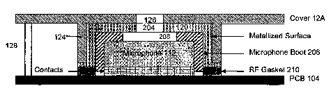
may force the placement of microphone 112 to be closer to such antennae than
preferred (at
least for RF interference reasons).
[0045] To further assist in shielding microphone 112, radio frequency (RF)
shield can
120 is provided to cover microphone 112 on PCB 104. Shield can 120 provides an
electromagnetic shield to isolate microphone 112 from electromagnetic
interference. Such
interference may originate from signals received and generated by either
antenna 154 or 156.
Shield can 120 has aperture 204 therein to allow audio signals entering
opening 126 to
ultimately enter shield can 120 and be provided to microphone 112. The size
and shape of
aperture 204 may be designed to meet acoustic and shielding requirements as
needed. In
particular, the size should be sufficiently small to still provide effective
RF shielding, but
sufficiently large to allow acoustic signals to pass into its interior to
reach microphone 112.
CA 02550887 2009-05-12
- 13-
In one embodiment, aperture 204 is round and has a diameter of approximately 1
to 2 mm.
Shield can 120 is preferably made of metal and is shaped to completely enclose
microphone
112, but for aperture 204, when microphone 112 is mounted onto PCB 104. In the
embodiment it has a thickness of approximately 0.2 mm, although other
thicknesses can be
employed. Shield can 120 is oblong in shape, but any suitable shape may be
used which can
cover microphone 112. At the bottom edge of shield can 120, a laterally
extending flange
may be provided to create a larger gasket area for placement tolerance and
more reliable
electrical contact. Microphone boot 206 is provided as a spacer between shield
can 120 and
microphone 112. It is made of a compressible, non-conductive material, like
rubber and is a
generally thin covering shaped to cover enough of the body of microphone 112
to prohibit or
impede contact between microphone 112 and shield can 120. Boot 206 does not
necessarily
have to cover all contact points between microphone 112 and shield can 120.
Boot 206 also
provides acoustic sealing and vibration isolation for microphone 112. Boot 206
has an
aperture 208 on its upper surface which is in approximate alignment with
apertures 204 and
122, thereby allowing any ambient sound signals to pass through boot 206 and
reach
microphone 112. The various apertures may be shaped and sized to provide
placement of the
external port away from the microphone itself to further enhance microphone
placement with
respect to the antennae location and the resulting RF interference, provided a
clear path is
provided for the ambient sound to reach microphone 112. This may also provide
flexibility
in location and size of external hole 126 in cover 12.
[00461 In the embodiment, microphone 112 may be soldered or fixed to PCB 104.
In
other embodiments, microphone 112 may be held in place on PCB 104 using a
friction fit of
boot 206, can 120 and elements of cover 12A. On PCB 104, RF gasket 210 is
provided on its
CA 02550887 2009-05-12
-14-
surface and surrounds the location footprint of microphone 112 on PCB 104. It
defines a
perimeter around the footprint which aligns with the boundary defined by
bottom edge of
shield can 120. As such, shield can 120 rests on top of gasket 210 when in
place. In order to
provide an RF seal, gasket 210 is preferably conductive and as such, may be
made from a
conductive material like GS 8000. PCB 104 may have at least one exposed
contact pad
underneath the perimeter of gasket 210 to provide an electrical connection
with gasket 210
and shield can 120 to an electrical circuit in PCB 104. The circuit may simply
be a
connection to an interior ground plane in PCB 104 to assist in the RF
shielding.
[00471 In the interior of cover 12A, walls 124 descend vertically inward from
the interior
ceiling of cover 12A to define interior cavity 214, which is shaped to provide
a snug fit
around a part (or even all) of RF shield can 120 and to assist in aligning can
120 above
microphone 112. In the present embodiment, there are four walls 124 which are
located on
each side of rectangular microphone 112. In other embodiments, other
arrangements of size
and number of walls (e.g. two or three walls) may be provided. Although they
are connected
in the shown embodiment, they may not necessarily be connected. In other
embodiments,
corner sections may be provided which descend from the interior ceiling.
Aperture 126 in
cover 12A in the top surface of cavity 214 allows audible signals to enter
from the outside
environment of device 10 to its interior and microphone 112. It will be
appreciated that other
physical wall-like structures may be provided within cover 12A and / or PCB
104 to align
shield can 120 about microphone 112. To assist in the shielding of microphone
112 from
unwanted RF signals the exposed surface of cavity may be coated with a
metallized material.
[00481 To assemble the relevant components, microphone 112 is placed in its
final
position with its connections aligning with the corresponding pads on PCB 102.
As noted
CA 02550887 2009-05-12
-15-
earlier, microphone 112 is typically not soldered onto PCB 102. Boot 206 is
fitted over
microphone 112. Then shield can 120 is fitted over boot 206. Shield can 120,
boot 206 and
microphone 112 may be assembled together in whole or in part prior to
insertion on PCB
102. When cover 12A is fitted in place with cover 12B over PCB 102, interior
cavity 214
contacts the top surface of shield can 120. The dimensions and shapes of PCB
102, covers
12A and 12B, shield can 120, boot 206, gasket 210 and microphone 112 are
defined such that
cover 12A presses inward on shield can 120 which compresses boot 206 which
provides
inward pressure on microphone 112, thereby providing an inward friction fit
for microphone
112 onto PCB 104 into its intended position about its contact pads. A
fastening means, such
as screw 128, provides a tight binding mechanism to keep cover 12A and 12B
locked
together with all elements appropriately secured within, in place.
Alternatively, a set of
engageable latches and hooks may be provided among the covers 12A and 12B and
PCB 102
to provide a snap-fit arrangement of the pieces. Although they are not shown,
antennae 154
and 156 are typically located at one end of PCB 102.
[00491 As shown in Fig. 5, the lateral width of gasket 210 is wide enough to
support the
bottom edge of shield can 120, including its bottom flange. Walls 124 are
positioned to fit
relatively tightly over shield can 120 and extend to abut against the top
surface of the
exposed bottom flange of can 120. It will be appreciated that in other
embodiments, the
physical interface between elements may have different shapes and abutments.
When all
elements are assembled, all apertures 126, 204 and 208 are in approximate
alignment
allowing audible signals to travel from the outside of device 10 to microphone
112.
[00501 Referring to Fig. 6, another embodiment is shown where an additional
gasket
130(2) is provided between the top of RF shield can 120(2) and the inner
surface of interior
CA 02550887 2009-05-12
-16-
cavity 214. The footprint of gasket 130(2) is shaped to have a larger open
area for its
aperture 132 than the corresponding apertures for the other elements. As such,
the shape and
size of aperture 132 can be varied to provide different Helmholtz resonators
by the space
bounded by the lateral edges of aperture 132, the bottom of the interior cover
of cover
12A(2) and the top of shield can 120(2). One use of the resonator is to
provide pre-emphasis
to high frequency signals received through aperture 132. For calculation
purposes, one or
both of the other apertures may be considered to be part of the resonator. To
assist in fixing
elements in place, the top and bottom of gasket 130 may have an adhesive
applied thereto to
assist in affixing it to its neighbour. Gasket 210(2) is shaped to align with
the straight bottom
of shield can 120(2). The walls 124(2) do not extend fully inward such that
they abut against
either PCB 102 or RF gasket 210(2). In other embodiments, other shapes can be
defined for
the differing elements.
[00511 It will be appreciated that in other embodiments, one or more of the
above
components may be modified in their sizes and shapes to meet specific
operational
requirements. Also, the order of arrangement of the components can be
modified. For
example, referring to Fig. 7, a further embodiment is shown where RF shield
can 120(3) is
placed underneath boot 206(3). Gasket 130(3) is located between the upper
surface of
microphone 112 and the ceiling of RF shield can 120(3). Interior cavity 214(3)
is defined to
have additional spacers 132 on the exterior perimeter of its area to provide
additional space
in cavity 214(3) underneath cover 12A. Cavity 214(3) defines a Helmholtz
cavity in a
similar manner as described above.
[00521 It will be appreciated that one feature of the embodiments is a system
which
allows microphones to be mounted onto a PCB and be shielded from RF signals
without
CA 02550887 2009-05-12
-17-
necessarily having to solder the microphones to the PCB. It is biased inward
or held in place
by a fastener. As noted, one method of securing the shield to the PCB is to
use a friction fit
between the PCB and the cover of the device. However, in other embodiments,
other devices
or techniques may be used to impart inward friction or pressure onto the
shield. For
example, a RF shield can may be provided with latches or receptacles for
latches that engage
with corresponding elements on the PCB or the lower cover to secure the shield
in place.
Also, the shield may be held down with screws secured into the PCB. It will be
appreciated
that there are other securing techniques which could be used that do not
involve soldering.
[00531 In other embodiments, a microphone and a shield can may be placed on
the back
side of a PCB of device 10. Therein, a back cover for device 10 is provided
with an
appropriate interior cavity (similar to one described above) to impart an
inward, upward
pressure on the shield can to press it against the PCB and the microphone to
hold the
microphone in place. It will be seen that such embodiments operate in a
similar manner to
embodiments described above, but for relevant components being placed on the
back side of
the PCB and mounting and alignment features being provided in the back cover
for device
10.
[00541 Although the invention has been described with reference to certain
specific
embodiments, various modifications thereof will be apparent to those skilled
in the art
without departing from the scope of the invention as outlined in the claims
appended hereto.