Note: Descriptions are shown in the official language in which they were submitted.
CA 02550952 2006-06-27
- 1 - 2005P03152 US-rai
Circuit arrangement and method for operating at least one L$D
and at least one electric lamp
Technical field
The present invention relates to a circuit arrangement for
operating at least one LED (light-emitting diode) and at least
one electric lamp having at least one first filament and one
second filament, comprising a first terminal for the first
filament and a second terminal for the second filament of the
electric lamp and a lamp supply unit for supplying power to the
electric lamp.. It also relates to a corresponding operating
method for at least one LED and at least one electric lamp
using such a circuit arrangement.
Prior art
The principal problem on which the present invention is based
consists in both electric lamps, for example fluorescent lamps,
and LEDs being operated in an illumination unit in order to
achieve particular visual effects, for example in order to vary
the color temperature. For this purpose, two ballasts are used
in the prior art, to be precise a ballast for the light-
emitting diodes and a second ballast for the fluorescent lamps.
In this case, the manufacturer of such an illumination unit
connects the two ballasts to the system connection of the
illumination unit via corresponding lines. Disadvantages of
this' known solution are the complexity in terms of wiring
involved for the manufacturer of such an illumination unit and
the space requirement involved for the two ballasts of such an
illumination unit.
Summary of the invention
The object of the present invention consists in developing the
circuit arrangement cited at the outset or the operating method
CA 02550952 2006-06-27
- 2 - 2005P03152 US-rai
cited at the outset such that a reduction in the wiring
complexity and a reduction in the space requirement for the
units) used to drive the electric lamps) and the light-
emitting diodes) are possible.
In principle, the present invention is based on the knowledge
that the disadvantages of the prior art can be overcome if the
at least one electric lamp and the at least one LED are
operated with one and the same ballast. This is because,
firstly, this only requires this one ballast to be wired to the
system connection. Secondly, such a ballast requires less space
than the two ballasts which were required in the procedure in
accordance with the prior art, in particular if specific
components are used both for the operation of the at least one
electric lamp and for the operation of the at least one LED.
If the current through the electric lamp is regulated, this
also results in the advantage that the luminous flux of the
individual LEDs is fixed within a predetermined tolerance
irrespective of the number of LEDs connected. Furthermore, with
the circuit arrangement according to the invention, the LEDs
can also be used to establish whether the electric lamp is
intact. This is because a current flow takes place to the
second terminal for the second filament of the electric lamp
only in the case of an intact electric lamp, i.e. the sum of
the currents to the second filaments is not equal to zero, with
the result that the at least one LED only illuminates when the
electric lamp is not defective.
One preferred embodiment is characterized by the fact that the
LED supply unit has an input and an output, the input and the
output being DC-isolated from one another in terms of their
potentials. The DC-isolation ensures that no direct current is
transmitted from the input of the LED supply unit to the output
of the LED supply unit . Owing to these measures, it is easily
possible to adhere to the safety regulations for the operation
CA 02550952 2006-06-27
- 3 - 2005P03152 US-rai
of LEDs envisaged for some applications or in various
countries.
The LED supply unit particularly preferably comprises a
transformer, whose primary side is coupled to the second
terminal. During operation, an alternating current having a
constant amplitude therefore flows through the primary side of
the transformer and consequently also on the secondary side of
the transformer, By selecting the turns ratio, it is possible
to establish the amplitude of the alternating current on the
secondary side. The current through the LED determines the
color and the brightness of the light output by the LED. In
this case, a capacitance is preferably connected in parallel
with the secondary side of the transformer. Owing to this
measure, it is possible for the current through the at least
one light-emitting diode to be set independently of the turns
ratio of the transformer.
As an alternative to the transformer, the LED supply unit may
comprise a capacitive coupling-out apparatus, which is coupled
to the second terminal. In this case, the light-emitting diodes
are preferably operated via two capacitors in parallel with a
coupling capacitor, which is required for the operation of the
electric lamp. In this case, the current through the LEDs is
less than or equal to the current through the electric lamp. In
this case, the capacitive coupling-out apparatus likewise
ensures that no direct current is transmitted from the input to
the output of the LED supply unit. In terms of good insulation
properties, possible capacitive coupling-out apparatuses are,
in particular, so-called X or Y capacitors.
Furthermore, a voltage limitation apparatus, in particular a
zener diode is preferably connected in parallel with the at
least one LED. This voltage limitation apparatus protects the
at least one light-emitting diode against overload since, in
the case of most light-emitting diodes, the power consumed
increases with the operating voltage. In particular in the case
CA 02550952 2006-06-27
- 4 - 2005P03152 US-rai
of a plurality of series-connected LEDs, application faults of
a circuit arrangement according to the invention can thus be
prevented: owing to the voltage limitation apparatus being
suitably dimensioned, the total number of LEDs which can be
operated without an overload on the circuit arrangement and/or
the total power which can be converted in the LEDs can be
limited.
The LED supply unit preferably also comprises a rectifier,
which is designed to provide a rectified signal at the output
of the LED supply unit, i.e, at the terminal at which the at
least one LED is connected to the LED supply unit.
The second filament of the electric lamp is preferably the cold
filament.
It is further preferred if the input of the LED supply unit is
coupled between the second terminal for the electric lamp and a
reference potential, in particular ground.
When connecting a plurality of LEDs to a circuit arrangement
according to the invention, these LEDs are preferably connected
in series.
In order to smooth the current in the LEDs, a smoothing
inductor can advantageously be introduced in series in the
current path of the LEDs.
Further advantageous embodiments are described in the dependent
claims.
The preferred embodiments and advantages described above with
reference to the circuit arrangement according to the invention
apply correspondingly to the operating method according to the
invention.
Brief description of the drawings
CA 02550952 2006-06-27
- 5 - 2005P03152 US-rai
Three exemplary embodiments of a circuit arrangement according
to the invention will now be described below with reference to
the attached drawings, in which:
figure 1 shows a first exemplary embodiment of a circuit
arrangement according to the invention;
figure 2 shows a second exemplary embodiment of a circuit
arrangement according to the invention; and
figure 3 shows a third exemplary embodiment of a circuit
arrangement according to the invention.
Preferred embodiment of the invention
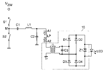
Figure 1 shows a schematic illustration of a first exemplary
embodiment of a circuit arrangement according to the invention,
for reasons of clarity only the components which are relevant
to the invention being illustrated. A so-called intermediate
circuit voltage UZW which, as is generally known, is produced
from the system voltage and is generally of the order of
magnitude of 400 V, is applied to the series circuit comprising
a first switch S1, implemented by a first bridge transistor,
and a second switch S2, implemented by a second bridge
transistor. In the present exemplary embodiment, a half-bridge
circuit is used as the bridge circuit . However, as is obvious
to a person skilled in the art, the invention can also be
implemented using a full-bridge circuit or.even in the case of
conventional ballasts, i.e. ballasts without a bridge circuit.
The switches S1 and S2 are driven, in a known manner, so as to
realize an inverter. A center point M of the bridge circuit is
defined between the two switches S1, S2. The bridge center
point M is connected to an electric lamp LP, in particular a
fluorescent lamp, via a coupling capacitor C1 and an inductance
L1. A resonant capacitor C2 is arranged in parallel with the
lamp LP. The circuit arrangement comprises a first terminal Al
CA 02550952 2006-06-27
- 6 - 2005P03152 US-rai
for a first filament W1 and a second terminal A2 for a second
filament W2 of the lamp LP. As can be seen from the drawing,
the filament W1 is the hot filament, and the filament W2 is the
cold filament of the lamp LP. An LED supply unit 10 is coupled
to the second terminal A2 for the second filament W2 of the
electric lamp and is designed to supply power to the at least
one LED. The LED supply unit 10 comprises a transformer Tr
having a transformation ratio U, whose primary side is coupled
between the terminal A2 of the electric lamp LP and the ground
potential. The secondary side of the transformer Tr is
connected in parallel with a capacitor C3, which makes it
possible to set the current through the at least one LED
irrespective of the turns ratio U of the transformer Tr. The
capacitor C3 is coupled to the input of a rectifier, which
comprises the diodes D1 to D4, the output of the rectifier
being coupled to the LED. By selecting the transformation ratio
i1 of the transformer Tr and selecting the capacitance of the
capacitor C3, it is possible to set the properties of the light
output by the LED, in particular the light color and the
brightness. In order to safeguard the LED against overload
owing to excessively high voltages, in particular during
starting operation of the electric lamp LP, a voltage
limitation apparatus, in this case a zener diode Z1, is
arranged in parallel with the LED.
Figure 2 shows a schematic illustration of the relevant
components of a second exemplary embodiment of a circuit
arrangement according to the invention, in which the same
reference symbols which have already been introduced with
reference to figure 1 are used for components which correspond
to those in figure 1. In the exemplary embodiment illustrated
in figure 2, the LED supply unit 10 comprises a capacitive
coupling-out apparatus, which is coupled to the second terminal
A2 of the lamp LP. This second coupling-out apparatus comprises
two capacitors C5, C6, which are operated in parallel with a
coupling capacitor C4 for the lamp LP. At the times at which
the potential at the terminal A2 is greater than the ground
CA 02550952 2006-06-27
- 7 - 2005P03152 US-rai
potential, a current accordingly flows via the capacitor C5,
the diode D1, the LED, the diode D4 and the capacitor C6. At
the times at which the potential at the terminal A2 is less
than the ground potential, a current flows via the capacitor
C6, the diode D2, the LED, the diode D3 and the capacitor C5.
Figure 3 shows a schematic illustration of the relevant
components of a third exemplary embodiment of a circuit
arrangement according to the invention, in which, in turn, the
same reference symbols which have already been introduced with
reference to figure 1 are used for components which correspond
to those in figure 1. In the exemplary embodiment illustrated
in figure 3, the inductance L1 in the supply line of the
electric lamp LP represents the primary winding of a
transformer, whose two secondary windings L21 and L22 are
arranged, together with the capacitors C7 and C8, in series
with the respective terminals A1, A2 for the lamp LP for the
purpose of preheating the lamp. In order to prevent the
transmission of current to the LED during the preheating
operation of the electric lamp LP, the primary side of the
transformer Tr has a first winding and a second winding, the
first winding being coupled to the first feedline of the
terminal A2, and the second winding being coupled to the second
feedline of the terminal A2.