Note: Descriptions are shown in the official language in which they were submitted.
CA 02551559 2006-06-23
WO 2005/062421 PCT/GB2004/005460
-1-
AN ANTENNA HAVING CONTROLLABLE EMISSION OF RADIATION
Field of the Invention
The present invention relates to an antenna with improved capability in
locking
onto a signal. The antenna is particularly suitable for use as part of a
mobile
telephone or any wireless device.
Background to the Invention
The growth in the market for hand-held communication devices, not physically
connected to a communication land line has, in recent years, been consistent
and
large. In particular, mobile telephones are now not only capable of allowing
voice
IO communication but also the transmission of moving images, virtually in real
time.
As there is no physical connection between a device and a land line,
communication or information is transmitted by means of electromagnetic
radiation signals. The means to transmit said information is usually an
antenna
attached to a device. For a device to transmit information, a low power signal
is
emitted from the device via the antenna. The signal is received by a tower
which
forwards the signal on. The tower can increase the power of the signal and
cause
it to be transmitted over large distances. The reception of the signal by a
second
device is essentially the reverse of the above described process in that a
signal
transmitted from a tower is received by the antenna of the mobile device and
the
information carried by the electromagnetic radiation is converted to the form
of
the output e.g. sound, text, images etc.
CA 02551559 2006-06-23
WO 2005/062421 PCT/GB2004/005460
-2
Whatever the type of information being communicated, the problem remains of
enabling a device to continue in contact with a transmission / reception
tower. A
key aspect of this is ensuring that the orientation of the signal transmitted
by the
mobile device is such that it is capable of being received by the tower. If
the
signal transmitted from the mobile device is not in the direction of the tower
then
the signal will not be received by the tower, irrespective of the power of the
signal
transmitted.
In an attempt to overcome this limitation, devices have been produced with a
plurality of antennae and a processor to switch between antennae to make sure
that the connection is not lost. The disadvantage of this approach is that to
include a plurality of antennae increases the complexity of the device and its
cost
of manufacture.
It is an object of the present invention to provide a single antenna to
overcome the
above disadvantages and provide an improved device.
Summary of the Invention
According to a first aspect of the invention there is provided:
an antenna for use in a communication device;
the antenna having a transmission/receiving element, the element being adapted
to
transmit and receive a radiation pattern;
the element being supported on a dielectric material layer;
wherein the orientation of a radiation pattern transmitted or able to be
received by
the element is controlled electronically.
The antenna is simpler and cheaper to manufacture than conventional antennae.
The need to include complex electronic circuitry (such as phase shifters and
their
associated control) to activate and deactivate antenna elements as in the case
of a
CA 02551559 2006-06-23
WO 2005/062421 PCT/GB2004/005460
-3-
multiple element antenna system is therefore obviated.
The transmission/receiving element preferably includes at least one loop. An
element having a spiral configuration is particularly preferred with a
rectangular
spiral being especially preferred. Alternatively, the spiral can have, a
circular,
triangular, trapezoidal configuration.
Conveniently, dielectric material from which the layer is formed dielectric
material has a dielectric constant of from 2-10. Typically the value is from
3.4 -
3.9. Preferably the thickness of the dielectric material layer is less than
20mm, and
particularly preferably 10-l4mm. The dielectric material layer optionally
comprises two layers of dielectric materials of different dielectric constant.
Conveniently the dielectric material layer is itself supported on a conductive
layer,
the conductive layer being itself optionally backed by an insulating medium.
The use of at least one low loss radio frequency (RF) switch (for example
micro
electromechanical switch (MEM) or PIN diode) will introduce phase shifts in
the
signal travelling on the transmission element by shorting or open-circuiting
the
element. This has the effect of changing the radiation pattern of the antenna.
Hence the radiation pattern can be made adaptive by using multiple switches.
Advantageously the dielectric constant of one or both of the dielectric
material
layers is variable. Variation of the dielectric constant can be by means of an
applied d-c voltage which causes a change in the dielectric constant of the
dielectric material. Since the guided wavelength along the spiral arm is
dependant
on the value of the dielectric constant, changing the dielectric constant
causes a
change in the angle of the emitted beam. Particularly preferably the applied
voltage is from 5-SOV with 5-20V being especially preferred. Optionally, a
liquid
crystal is embedded within the dielectric material. Variation of the magnitude
of
the applied voltage therefore causes a change in the angle of an emitted beam
of
radiation, and allows very rapid switching without the use of moving parts or
continual breakage and formation of a circuit. The communication device can
therefore readily transmit in the direction required to remain in contact with
a
CA 02551559 2006-06-23
WO 2005/062421 PCT/GB2004/005460
-4-
receiver.
According to a second aspect of the invention there is provided a
communication
device, the device including an antenna including a transmission element
having
at least one loop, the device further including one or more switches to effect
a
break in the transmission element. Preferably, the transmission element has a
spiral configuration.
Brief Description of the Drawings
The invention will now be described with reference to the accompanying
drawings which show by way of reference two embodiments of an antenna
element of a communication device. In the drawings:
Figure 1 illustrates the emission of electromagnetic radiation from a mobile
phone;
Figures 2A and 2B illustrate two views of an antenna;
Figures 3A and 3B illustrate the beam emitted or received by the antenna of
Figure 2 and a standard antenna respectively;
Figure 4 illustrates an open circuit switch antenna arm; having four open
switches;
Figure 5 is a table illustrating switching configurations of the antenna arm
in
Figure 4;
Figure 6 is an x-y plot showing 6max and cpma,; for the switching
configurations in
Figure 5.
Figures 7 and 8 show the gain and the VSWR respectively for the switching
configurations of Figure 5;
Figure 9 illustrates the radiation pattern for the maximum beam directions for
switch configurations 4 and 13 shown in Figure 5;
CA 02551559 2006-06-23
WO 2005/062421 PCT/GB2004/005460
-5-
Figure 10 illustrates an antenna having four shorting switches;
Figure 11 is an x-y plot showing 6maX and cpmah for shorting switch
configurations
in Figure 5.
Figures 12 and 13 show the gain and the VSWR respectively for shorting switch
configurations of Figure 5;
Figure 14 illustrates the radiation pattern for the maximum beam directions
for
shorting switch configurations 4 and 13 shown in Figures 5;
Figure 15 illustrates an antenna having a dielectric layer of varying
dielectric
constant; and
Figure 16 is a x - y plot of 6maX and cpmaX against dielectric constant.
Detailed Description of the Invention
The following example is one embodiment of the invention. It will of course be
understood that there are a number of ways of incorporating the invention
which
do not depart from the inventive concept.
In Figure 1, an antenna 10 which emits a signal in the form of a beam of
electromagnetic radiation. The beam is capable of carrying sufficient
information
for a decoding device to reproduce sound, text or visual images. The beams
11A,B,C are inclined at different angles relative to each other. The angle of
the
beam is variable and thus beams 11A,B,C are just illustrative examples. This
feature maximises the possibility of the element either transmitting to a
tower or
alternatively receiving a message therefrom.
In determining the angle of the beam to be used, a processing and signal
strength
detector 12 monitors the strength. Should the detector 12 determine the need
to
transmit using a different beam 11, the detector 12 sends a signal to a
circuit 13
which controls the direction of the beam 11.
CA 02551559 2006-06-23
WO 2005/062421 PCT/GB2004/005460
-6-
The circuit 13, should it be so required, switches the angle of the beam 11 so
as to
orient it towards the direction of the strongest signal. In this manner
contact with
a transmission tower is maintained and kept strong.
An embodiment of an antenna suitable to emit the beam pattern of Figure 1 is
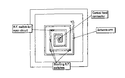
shown in Figure 2A. In Figure 2A, the antenna 20 has a copper transmission
element 21 having the form of a single-armed, rectangular spiral. The
transmission element 21 is approximately 1.4 mm wide and has an overall length
of approximately 290 mm. A support 25 for the transmission element 21, is made
of a dielectric material, Roger Ro-4350B having a dielectric constant of
approximately 3.7. In order to produce a good signal the antenna's thickness
is
approximately l2mm. For convenience the dielectric material is formed into a
square having a side length of approximately 51.3 mm.
The dielectric material, itself is backed by a conducting plane and where
useful,
for example to improve ease of incorporation of the antenna within a device,
the
conducting plane itself can be backed by a further layer formed of
electrically
insulating material.
One of the functions of the transmission element 21 is to emit, upon
energisation
by an electric current, a beam of electromagnetic radiation, carrying
information.
The point 22 is the feeding point of the antenna 10. Shorting RF switches 23
and
open circuit switch 24 are used to introduce a phase shift in the signal
travelling
on the antenna arm. The phase shift effects a movement in the angle of the
beam
radiated from the antenna. With the use of multiple switches any desired
variation
in the angle of the beam radiated can be achieved. Thus, making the whole of
the
antenna radiation pattern adaptive.
The dielectric constant of the dielectric material from which the support 25
is
made will typically have a dielectric constant of from 2-10. It has been found
that
a range of 3.4-3.9 for the dielectric constant gives an efficient and
effective
antenna. A number of materials known in the art, therefore suggest themselves
as
being suitable for use.
CA 02551559 2006-06-23
WO 2005/062421 PCT/GB2004/005460
_'7_
The thickness of the antenna 20 produced depends on a number of factors such
as
the operating frequency, the dielectric material used, the impedance of the
feeding
point and the dimensions of the unit into which the antenna is incorporated.
For
example, the usage of a material, for the support, which has a higher
dielectric
constant enables a thinner antenna to be used. Antenna contemplated in the
present invention have a thickness of less than 20 mm. More typically the
thickness of an antenna can be 10-l4mm.
Different shapes are possible for a transmission element whilst retaining at
least
one substantially 360° turn within the configuration. Although the use
of a
rectangular spiral allows easier numerical analysis of the signal, a circular
spiral,
trapezoidal or a triangular transmission element can be used.
In order to provide a switching function, a switch which allows both rapid
switching and which is robust is required. In practice such a switch is
provided by
a microelectromechanical switch (MEMS), a pin diode or any radio frequency
(RF) switch. In use, the particular type of switch is chosen to suit the
particular
dimensions of the antenna.
It has been found useful to be able to perform small changes of the angle of
an
emitted beam. In one embodiment, illustrated in Figure 2A. This has been
achieved by introducing a number of breaks of circuit within the spiral arm of
the
transmission element. Such breaks are provided by means of switches. As can be
visualised, the circuit can be made shorter or longer in a series of finite
steps by
activation or deactivation of the switches. By controlling which switches are
open
and closed, the angle of beam emission is thereby altered as and when
required. It
will be appreciated that increasing the number of switches incorporated into
an
antenna arm, decreases the lengths of the steps between the different
effective
lengths of the antenna. A greater number of switches therefore can lead to a
smoother change in the angles at which radiation is emitted.
An example of the change induced in a transmitted beam is given in Figures 3A,
3B, in which the arrows indicate the direction of maximum emitted radiation.
In
Figure 3B the emitted radiation is predominantly axial, that is directed along
the
CA 02551559 2006-06-23
WO 2005/062421 PCT/GB2004/005460
_g_
axis vector of the spiral. On application of the switches, the vector is
rotated so
that its direction is no longer in line with said axis vector.
On using the switching antenna as described above it has been found that the
Voltage Standing Wave Ratio (VSWR), which is a measure the ratio of forward
power to reflected, power, normally remains under 2, indicating that the power
required to transmit a signal is not greatly affected by switching. For the
limited
number of switch configurations where the VSWR value rises above 2, extra
power can be channelled to signals to ensure signal stability. The gain for
various
configurations is relatively constant at around 7.SdB+/-l.SdB.
Figure 4 illustrates an antenna 40 having a series of open circuit switches
indicated at 1, 2, 3, and 4. The switches are approximately lmm wide and their
operation acts to shorten or lengthen the effective length of the antenna arm
41.
The effect of activating the switches is shown in Figures 5 - 9. As in the
exemplified disclosure, there are 4 switches, each of which can be either in
an on
or off position, there are essentially 16 different combinations or switching
configurations, and hence 16 effective lengths of antenna are possible. The 16
switching configurations are shown in the table in Figure 5. Figure 6 shows
the
emaX and ~pmax values obtained with the various switch configurations given in
Figure 5. The largest variation is seen to be in cpma,;, with a relatively
small
variation 8n,ax. The second sets of lines indicate results obtained from
theoretical
predictions cpmaX and 6maX and it can be seen that there is relatively good
correlation
between theory and experiment.
Figure 7 shows the gain (in dB) for the various switch configurations. The
VSWR is given in Figure 8 and shows that for the majority of switch
configurations, the VSWR is below 2. Finally, the radiation patterns in the
directions of the maximum beam for switch configurations 4 and 13 respectively
are shown in Figure 9.
Figures 10 - 14 illustrate results for the shorting switch mode of operation.
The
switch configurations are those shown in Figures 5.
CA 02551559 2006-06-23
WO 2005/062421 PCT/GB2004/005460
_9_
In a further embodiment of an antenna, the direction of the emitted beam is
altered
by applying a d-c voltage across the support from the transmission element to
the
conducting plane. A typical applied voltage is from 5-SOV, with a range of
from
5-20V being preferred. Application of the voltage changes the dielectric
constant
of the support material which alters the emitted beam's angle. In an aspect of
this
embodiment, a liquid crystal is embedded in the substrate material itself.
Variation of the voltage across the liquid crystal then causes the dielectric
constant to change.
For an example of such a device is shown in Figure 15. The antenna 150 has a
transmission element 151 which, as previously, is in the form of a
rectangular,
single-armed spiral. The dielectric substrate on which the element 151 lies
comprises two layers 152A, 152B which are of dii~ering dielectric constant ES
and
ar respectively. Typically the layer 152A is formed of a synthetic / ferro-
electric
material. Application across the antenna therefore of a voltage V causes the
dielectric constant ss of the material on the layer 152A to change. The net
dielectric constant of combined dielectric layers, s"et 1S a function of as
and ar.
Changing $S therefore changes $nzt and causes the effective guided wave length
~,g
within the element 151 to be altered and thereby the angle at which radiation
is
emitted from the antenna.
Figure 16 illustrates the effect of changes of dielectric constant on the
angle of
transmission. In Figure 16, the axial and radial (with respect to the spiral
transmission element) components of the transmitted radiation have been
separated and are designated by 8",aX and cp",aX respectively. It will be
noted that as
Enec is changed then the angles of Amah and cpmaX are also changed. Across the
illustrated s"etvalues, 6maX exhibits a variation of 19° and cp",aa a
variation of 237°.
This compares with a range of 39° and 174° for the switching
method illustrated
earlier. Thus the switching method is capable of inducing greater variations
in
emax and changing the dielectric constant induces greater variations in cpmax.
It can
be envisaged that a combination of the switching method and the dielectric
method can be used to bring about the widest variations of both 8 and cp
within a
single device.
CA 02551559 2006-06-23
WO 2005/062421 PCT/GB2004/005460
-10-
It will of course be understood that the invention is not limited to the
specific
details described herein, which are given by way of example only, and that
various modifications and alterations are possible within the scope of the
appended claims.
10