Note: Descriptions are shown in the official language in which they were submitted.
~ ' I
CA 02552417 2006-06-30
Description
OPTICAL FUNCTIONAL CIRCUIT
Technical Field
[0001] The present invention relates to an optical
functional circuit , and more particularly, to an optical
functional circuit which uses a holographic wave
propagation medium to propagate a wave holographically
through multiple scattering in accordance with a
two-dimensional refractive index distribution.
Background Art
[0002] In an optical communication field, as an
optical circuit which can easily attain the branch and
interference of light , an integrated optical part using
an optical waveguide structure has been developed. In
the integrated optical part using the characteristic as
the wave of the light, an optical waveguide length is
adjusted to make the manufacturing of an optical
interferometer easier, or a circuit processing technique
in a semiconductor ffield is applied, which makes the
integration of the optical parts easier.
[0003] Such an optical waveguide structure is an
"optical confinement structure" where with regard to the
light propagating through the optical waveguide, the
spatial distribution of refractive indexes is used to
CA 02552417 2006-06-30
~ ,
- 2 -
attain a spatial optical confinement. In order to
constitute the optical circuit, an optical wiring and
the like are used to connect respective components in
cascade arrangement. For this reason, an optical path
length of the optical waveguide circuit must be longer
than an optical path length required to generate an
interference phenomenon and the like inside the optical
circuit. This results in a problem that the optical
circuit itself is extremely large in scale.
[0004] For example, when a typical arrayed waveguide
grating is exemplified, a plurality of lights having a
wavelength (~.~ ) inputted from an input port are repeatedly
branched and coupled by a star coupler having a slab
waveguide. Then, the branched lights are outputted from
an output port . However, an optical path length required
to branch the light at a resolution of about 1/1000 of
a wavelength becomes several ten thousand times of a
wavelength of the light propagating through the waveguide.
Also, not only the waveguide patterning of the optical
circuit, but also the process for installing a wavelength
plate and the like to compensate the circuit property
depending on a polarized light state is required to be
performed (for example, refer to a Non-patent Document
1).
[0005] Also, in order to miniaturize the optical
circuit, the light is required to be strongly confined
in the waveguide. Thus, the optical waveguide is
~
~ r
CA 02552417 2006-06-30
..
required to have a very great refractive index difference .
For example, in the optical waveguide of a conventional
step index type, the optical waveguide is designed to
have the spatial distribution of the refractive indexes
so that a specific refractive index difference has a value
greater than 0.1~. When such a great refractive index
difference is used to carry out the optical confinement,
the degree of freedom of the circuit configuration is
limited. In particular, even if the refractive index
difference in the optical waveguide is attempted to be
attained by using a local W light irradiation, a
thermo-optic effect or an electro-optic effect or the
like, the change amount in the obtained refractive index
is about 0.1% at most.
[ 0006 ] Moreover, in a case of changing the propagation
direction of the light, when the optical path of the
optical waveguide is curved at a small curvature, the
propagating light is leaked out from the optical waveguide .
Thus, the circuit property is deteriorated such as an
increase in a transmission loss and the like. Therefore,
in order to change the propagation direction of the light,
the orientation must be gradually changed along the
optical path of the optical waveguide. Inevitably, the
optical circuit length becomes very long. As a result,
it is difficult to miniaturize the optical circuit.
[ 0007 ] Therefore , the optical circuit that is high
in efficiency and small in size is attained by using a
CA 02552417 2006-06-30
' ' ' I
4 -
wave propagation medium which is smaller than the optical
circuit usingthe conventional optical waveguide circuit
and holographic circuit and enables the optical signal
control of a sufficiently high efficiency under a gradual
refractive index distribution, namely, even under a small
refractive index difference.
[0008] However, in the wave propagation medium, in
accordance with the refractive index of each virtual pixel
defined by a virtual mesh, an optical signal, while
undergoing multiple scattering, is transmitted from the
input port to the output port. Thus, a manufacturing
error when the mesh-shaped pixel is generated causes the
leakage of the transmission light. Consequently, the
interference is generated between the propagation light
outputted to the output port and the leaked transmission
light of the same wavelength, and even if the wavelength
is different and the interference is not generated,
crosstalk is generated.
(0009] Also, the wave propagation medium transmits
an optical signal by using the effect of the interference .
Thus , a large angle cannot be given to the optical path,
and crosstalk is great. Since the effect of the
interference is different depending on the angle of the
incident light, the fact that the rate for the oblique
incident component is high leads to one reason of the
deterioration in crosstalk. In particular, in a region
where a beam diameter of the light near the input and
CA 02552417 2006-06-30
' i
- 5 -
output ports is small, the rate of the component obliquely
incident with respect to the propagation direction of
the light is great, which deteriorates the crosstalk.
There is a problem that the circuit property is further
deteriorated such that the transmission loss of the
optical circuit becomes greater because of the
deterioration of the crosstalk as mentioned above.
[0010] Moreover, the mesh-shaped pixel near the input
port and the output port in the wave propagation medium
can function as a kind of lens and collect the lights .
However, because of the mesh-shaped pixel, there is a
problem that the discrimination of a light focusing
position is difficult and the connection to a different
optical element is difficult.
[0011] Non-patent Document 1: Y.Hibino, "Passive
Optical Devices for Photonic Networks", IEIC'Trans.
Commun., Vol. E83-B No.lO, (2000).
Disclosure of the Invention
[ 0012 ] The first object of the present invention is
to provide an optical functional circuit in which a
holographic wave propagation medium is applied and a
circuit property is excellent such as small transmission
loss and crosstalk. Also, the second object is to provide
an optical functional circuit in which the connection
of an optical waveguide device, to which the holographic
wave propagation medium is applied, is made easier so
CA 02552417 2006-06-30
- 6 -
that the transmission loss and the crosstalk are small.
[ 0013 ] In order to attain such objects, the optical
functional circuit in which a plurality of circuit
elements are formed on a substrate includes a wave
propagation medium, which converts an optical path of
the leakage light that is not emitted from a predetermined
output port of the circuit element so as to prevent the
leakage light from being coupled to a different circuit
element. This wave propagation medium is constituted
by an optical waveguide which is provided with a clad
layer formed on the substrate and a core embedded in the
clad layer, and a part of the optical waveguide is formed
in accordance with a refractive index distribution which
is multiple scattered.
[0014] Also, in the optical functional circuit
including the wave propagation medium, in order that among
optical signals made incident from an input port defined
in the wave propagation medium, a stray light that is
not emitted from a predetermined output port defined in
the wave propagation medium is not coupled to a different
output port, an optical axis of the input port and an
optical axis of the predetermined output port are arranged
so as not to be made coincident with each other.
[0015] Moreover, on the substrate, positioning
markers for defining input and output ports defined in
the wave propagation medium are formed. The positioning
markers , which are formed on members having optical parts
CA 02552417 2006-06-30
I
_ 7 _
optically coupled to the input and output ports and define
light focusing positions of the optical parts, and the
positioning markers for defining the ports are aligned,
thereby coupling the ports and the optical parts
optically.
[0016] Furthermore, on the substrate, monitoring
wave guides for defining input and output ports defined
in the wave propagation medium are formed from an end
facet on which the input port is formed to an end facet
on which the output port is formed. Optical fibers for
positioning, which are formed on members having optical
parts optically coupled to the input and output ports
and define light focusing positions of the optical parts,
and the monitoring waveguides are aligned, thereby
coupling the input and output ports and the optical parts
optically.
Brief Description of the Drawings
[ 0017 ] Fig . lA is a view explaining a basic structure
of a wave propagation medium;
Fig. 1B is a view explaining a basic structure of
a wave propagation medium;
Fig. 1C is a view explaining a basic structure of
a wave propagation medium;
Fig . 2 is a flowchart showing a calculation procedure
for determining a spatial refractive index distribution
of the wave propagation medium;
CA 02552417 2006-06-30
Fig. 3 is a view showing an optical
combining/splitting circuit according to an embodiment
of the present invention;
Fig. 4 is a view showing a transmission spectrum
of the optical combining/splitting circuit;
Fig . 5 is a view showing a removing method of a leakage
light in an optical branching circuit;
Fig. 6 is a view showing an insertion loss of the
optical branching circuit to which the removing method
of the leakage light according to a first embodiment is
applied;
Fig . 7 is a view showing a removing method of a leakage
light in an MZ-type optical combining/splitting circuit;
Fig. 8A is a view showing a transmission spectrum
of the MZ-type optical combining/splitting circuit
without any stray light guide;
Fig. 8B is a view of a transmission spectrum of an
MZ-type optical combining/splitting circuit to which a
removing method of a leakage light according to a second
embodiment is applied;
Fig. 9 is a view showing a removing method of a stray
light according to a third embodiment of the present
invention;
Fig. 10 is a view showing a transmission spectrum
of an optical combining/splitting circuit according to
the third embodiment;
Fig. 11 is a view showing a removing method of a
CA 02552417 2006-06-30
r
- 9 -
stray light according to a fourth embodiment of the present
invention;
Fig. 12 is a view showing a removing method of a
stray light according to a fifth embodiment of the present
invention;
Fig. 13 is a view showing a removing method of a
stray light according to a sixth embodiment of the present
invention;
Fig. 14 is a view showing a removing method of a
stray light according to a seventh embodiment of the
present invention;
Fig. 15 is a view showing a configuration of an
optical waveguide device including an optical
combining/splitting circuit according to an eighth
embodiment of the present invention;
Fig. 16 is a view showing a configuration of an
optical waveguide device including an optical
combining/splitting circuit according to a ninth
embodiment of the present invention;
Fig. 17 is a view showing a configuration of an
optical waveguide device including an optical
combining/splitting circuit according to a tenth
embodiment of the present invention;
Fig. 18 is a view showing a configuration of an
optical waveguide device including an optical
combining/splitting circuit according to an eleventh
embodiment of the present invention;
CA 02552417 2006-06-30
i r .I
- 10 -
Fig. 19 is a view showing a configuration of an
optical waveguide device including an optical
combining/splitting circuit according to a twelfth
embodiment of the present invention;
Fig. 20 is a view showing a configuration of an
optical waveguide device including an optical
combining/splitting circuit according to a thirteenth
embodiment of the present invention;
Fig. 21 is a view showing a configuration of an
optical waveguide device including an optical
combining/splitting circuit according to a fourteenth
embodiment of the present invention; and
Fig. 22 is a view showing a configuration of an
optical line termination apparatus according to a
fifteenth embodiment of the present invention.
Best Mode for Carrying Out the Invention
[ 0018 ] Embodiments of the present invention will be
described below in detail with reference to the drawings .
An optical functional circuit in this embodiment is a
holographic wave propagation medium defined in a
plurality of scattering points and propagates a wave
holographically through multiple scattering in
accordance with a two-dimensional refractive index
distribution.
[0019] First, the basic concept of the wave
propagation medium used in the present invention is
CA 02552417 2006-06-30
' ,
- 11 -
explained. Here, since it is applied to an optical
circuit,"wave"propagating throughthe wave propagation
medium is "light . " It is noted that the theory related
to the wave propagation medium indicates the property
of a medium in accordance with a typical wave equation
and can be established in principle even in the typical
wave . In the wave propagation medium, in order to input
a coherent light pattern and output a desirable light
pattern, the refractive index distribution is determined
such that a phase difference between a forward propagation
light and a backward propagation light which propagates
through the wave propagation medium becomes small even
at any position in the wave propagation medium. The
desirable light pattern is outputted by the multipleX
repetition of a holographic control at a local level in
accordance with the refractive index distribution.
[0020] The basic structure of the wave propagation
medium according to this embodiment is explained with
reference to Figs . 1A to 1C . As shown in Fig . 1A, in an
optical circuit substrate 1, there is a design region
1-1 of an optical circuit constituted by the wave
propagation medium. One end facet of the optical circuit
is an incidence facet 2-1 to which an input light IN is
incident. The input lightIN propagates while undergoing
multiple scattering inside the optical circuit, which
is constituted by the wave propagation medium and has
a spatial refractive index distribution, and outputted
CA 02552417 2006-06-30
- 12 -
as an output light OUT from an exit facet 2-2 serving
as the other end facet. A coordinate z in Fig. lA is
a coordinate (z=0 is an incidence facet, and z=zg is an
exit facet ) in the propagation direction of the light ,
and a coordinate x is a coordinate in a lateral direction
relative to the propagation direction of the light. It
is noted that, in this embodiment, the wave propagation
medium is assumed to be made of dielectric material, and
the spatial refractive index distribution is attained
by setting a local refractive index of the dielectric
material constituting the wave propagation medium in
accordance with a theory which will be described later .
[ 0021 ] "Field" ( input field ) formed by the input light
IN is modulated in accordance with the spatial
distribution of the refractive indexes of the wave
propagation medium constituting the optical circuit and
converted into "field" (output field) formed by the output
light OUT . In other words , the wave propagation medium
of the present invention is the (electromagnetic) field
converting means for relating the input field and the
output field in accordance with the spatial refractive
index distribution. It is noted that, with regard to
the input field and output field, the field of the light
in a section ( the section along the x-axis in the drawing )
vertical to the propagation direction (the z-axis
direction in the drawing) in the optical circuit is
referred to as a (forward) propagation image (a
CA 02552417 2006-06-30 '
~I
- 13 -
propagation field or propagation light ) in that position
(x, z) (refer to Fig. 1B).
[0022] Here, "field" typically implies an
electromagnetic field or a vector potential of the
electromagnetic field. The control of the
electromagnetic field in this embodiment corresponds to
the change of the spatial refractive index distribution
installed in the optical circuit, namely, the
distribution of a dielectric constant. Although the
dielectric constant is given as a tensor, usually, the
transition between the polarized light states is not great .
Thus , even if only one component in the electromagnetic
field is targeted and a scalar wave approximation is
performed, an excellent approximation is attained.
Therefore, in this specification, the electromagnetic
field is treated as a complex scalar wave. It is noted
that, in "state" of the light, there are an energy state
(wavelength) and a polarized light state. Hence, when
"field" is treated as the representation of the state
of the light , the wavelength of the light and the polarized
light state can be contained.
[0023) Also, usually, in the optical circuit for
preventing the amplification and attenuation of the
propagation light, when the spatial distribution of the
refractive indexes is determined, the image ( the input
field) of the input light IN other than a focal point
is determined uniquely for the image (the output field)
CA 02552417 2006-06-30
r ' r
- 14 -
of the output light OUT. The field of the light
propagating to the side of the incidence facet 2-1 from
the side of the exit facet 2-2 as mentioned above is
referred to as a backward propagation image (a backward
propagation field or backward propagation light) (refer
to Fig. 1C) . The backward propagation image as mentioned
above can be defined for each position in the optical
circuit. That is, when the field of the light at any
position in the optical circuit is considered, if the
position is considered as the exit point of a virtual
"input light," similarly to the above-mentioned case,
the backward propagation image at the position can be
considered for the image of the output light OUT. In
this way, the backward propagation image can be defined
for each position in the optical circuit.
[0024] In particular, in the single optical circuit,
when the exit field is defined as the propagation field
of the incidence field, the propagation field and the
backward propagation field are coincident at any point
in the optical circuit . It is noted that the field is
the function on the targeted entire space. However, in
the case of "incidence field" or "exit field, " this implies
the section of the field on the incidence facet or exit
facet . Also, in the case of "field distribution, " when
a discussion is carried out with regard to a certain
particular section, this implies the section of the field
of the section concerned.
CA 02552417 2006-06-30
- 15 -
[0025] In order to explain a determining method of
the refractive index distribution, the use of symbols
is preferable in understanding. Thus, in order to
represent the respective amounts, the following symbols
are used. It is noted that the targeted light (field)
is not limited to the light in a single state. Hence,
in order to be able to target the light where the lights
in a plurality of states are superimposed, an index j
is given to the light in the individual state, and they
are typically represented.
[ 0026 ] ~ cp' (x) : j -th incidence field ( this is a complex
vector value function and defined in accordance with the
intensity distribution and phase distribution set on the
incidence facet , and the wavelength and polarized wave ) .
y' (x) : j-th exit field ( this is a complex vector
value function and defined in accordance with the
intensity distribution and phase distribution set on the
exit facet, and the wavelength and polarized wave).
It is noted that , with regard to cpj ( x ) and ~' ( x ) , unless
an intensity amplification, a wavelength conversion and
a polarized wave conversion are carried out in the circuit ,
the sum of the optical intensities are same (or the loss
of an ignorable level), and their wavelengths and
polarized waves are equal.
[ 0027 ] - {cp' (x) , ~' (x) } : input output pair ( a set of
a field of the input and output).
{ cp' ( x ) , ~' ( x ) } is def fined in accordance with the intensity
CA 02552417 2006-06-30
- 16 -
distribution and phase distribution on the incidence
facet and exit facet, and the wavelength and polarized
wave.
[0028] ~{nq}: refractive index distribution (a set
of values in an entire optical circuit design region) .
When one refractive index distribution is given to the
given incidence field and exit field, the field of the
light is determined. Thus, it is necessary to consider
the field for the entire refractive index distribution
given by the q-th repetitive calculation. Therefore,
assuming that (x, z ) is an uncertain variable, the entire
refractive index distribution may be represented as nq(x,
z ) . However, in order to distinguish from a value nQ(x,
z ) at a position (x, z ) , .{nq} is represented for the entire
refractive index distribution.
. [ 0029 ] ' ncore : a symbol indicating a value of a high
refractive index for a peripheral refractive index, such
as a core portion in the optical waveguide.
[ 0030 ] ' nclad= a symbol indicating a value of a low
refractive index for more, such as a clad portion in the
optical waveguide.
[ 0031 ] wp~ ( z , x, {nq} ) : a value of a field at the
position (x, z ) when the j-th incidence field cps (x) is
propagated until z in the refractive index distribution
{nq} .
~ ~' ( z , x, {nq} ) : a value of a field at the position
(x, z) when the j-th exit ffield ~~(x) is backwardly
CA 02552417 2006-06-30
. 5 , - 17 -
propagated until z in the refractive index distribution
{nq} .
[0032] In this embodiment, {nq} is given such that
the refractive index distribution becomes
cp' ( ze, x, {nq} ) _~' (x) or the state close thereto, for all
J.
[ 0033 ] "Input port" and "output port" are "regions"
where the fields on the incidence facet and the exit facet
are concentrated. For example, this is the region where
the optical intensity can be propagated to a fiber by
an optical fiber to the portion. Here, the intensity
distribution and phase distribution of the field can be
designed so as to be different between the j-th field
and the k-th field. Thus, a plurality of ports can be
installed on the incidence facet and the exit facet.
Moreover, when the set of the incidence field and the
exit field is considered, the phase generated by the
propagation between them is different depending on the
frequency of the light . Hence , the light whose frequency
is different (namely, the light whose wavelength is
different ) can be set as the different port , regardless
of whether or not the field shape including the phase
is equal or orthogonal.
[0034] Here, the electromagnetic field has the
wavelength and the polarized light state as the parameters ,
in the field of a real number vector value. However.
the value of the component is indicated by using a complex
CA 02552417 2006-06-30
.
- 18 -
number which is easy in typical mathematic treatment,
and the solution of the electromagnetic wave is
represented. Also, in the following calculation, it is
assumed that the intensity of the entire field is ruled
as 1. As shown in Fig. 1B and Fig. 1C, with regard to
the j - th incidence f field cp' ( x ) and exit f field ~' ( x ) , the
propagation field and backward propagation field, are
assumed to be the complex vector value functions at
respective positions and represented as ~~ ( z , x, {n} ) and
~'(z,x,{n}). Since the values of those functions are
changed in accordance with the refractive index
distribution {n}, the refractive index distribution {n}
becomes the parameter. From the definition of the
symbols, cp'(x)=cp'(O,x,{n}) and~'(x)=~'(ze,x,x{n}). The
values of those functions can be easily calculated by
the known method such as a beam propagation method and
the like , if the incidence f field cp' ( x ) , the exit f field
~' ( x ) and the ref ract five index dis tribut ion { n } are given .
[0035] A typical algorithm for determining the
spatial refractive index distribution will be explained
below. Fig. 2 shows a calculation procedure for
determining the spatial refractive index distribution
of the wave propagation medium. This calculation is
repeatedly executed. Then, the number of the repetitions
is represented by q. When the calculation is executed
untilthe(q-1)-th calculation,the(q-1)-th calculation
is illustrated. In accordance with a refractive index
CA 02552417 2006-06-30
- 19 -
distribution {nq_1} obtained by the (q-1 ) -th calculation,
with regard to each j-th incidence field c~~(x) and exit
field ~j(x), the propagation field and the backward
propagation field are calculated by a numerical
calculation, and the results are represented as
cp'(z,x,{nq_1}) and ~'(z,x,{nq_1}) respectively (step
S220).
[ 0036 ] In accordance with those results , a refractive
index nq(z,x) at each position (x, z) is calculated by
the following equation (step S240).
nq(z,x)=nq_1(z,x)-a~~Im[~j(z,x, {nq_1})*~~j(z,x,{nq_
1})l (1)
Here, the symbol [ ~ ] in the second term on the right-hand
side implies the inner product calculation, and Im[]
implies the imaginary component of the f field inner product
calculation result in []. It is noted that the symbol
[*] is the complex conjugate. The coefficient a is the
value after the value equal to or less than the fraction
of nq ( z , x ) is further divided by the number of the f field
sets , and this is the positive small value . The ~ j implies
the summing of the indexes j.
[ 0037 ] When the steps 5220 and S240 are repeated, if
an absolute value of a difference between the value
cp' ( ze,x, {n} ) on the exit facet of the propagation field
and the exit field ~' ( x ) becomes smaller than a desirable
error d~ (step 5230: YES), the calculation is ended.
[0038] In the above-mentioned calculations, the
CA 02552417 2006-06-30
20 -
initial value {no} of the refractive index distribution
may be suitably set. However, as this initial value {no}
is closer to an expected refractive index distribution,
the convergence of the calculation becomes accordingly
quick (step 5200). Also, when ~'(z,x,{nQ_1}) and
cp' ( z , x, {nq_1 } ) are calculated for each j , in a case of
a computer in which parallel calculations are possible,
they may be calculated for each j (namely, for each
~'(z,x,{nq_1}) and~j(z,x,{nq_1}), aclustersystemandthe
like can be used to make the efficiency of the calculation
higher ( step S220 ) . Also, if the computer is constituted
by a relatively small memory, in the summing portion about
the indexes j in the equation (1), the suitable j is
selected with regard to each q, and only the ~' ( z,x, {nq_1} )
and cpj ( z , x, {nq_1} ) , which correspond to it , can be ..
calculated to repeat the calculations thereafter ( step
S220).
[0039] In the above-mentioned calculations, if the
value of ~' ( z , x , { nq_1 } ) and the value of cpj ( z , x , { nq_1 } ) are
close, Im[~'(z,x,{nq_1})*~cpj(z,x,{nq_1})] in the equation
(1) becomes the value corresponding to the phase
difference. Then, reducing this value can obtain a
desirable output.
[0040] The determination of the refractive index
distribution can be expressed in a different word such
as an operation for determining a virtual mesh for the
wave propagation medium and determining a refractive
CA 02552417 2006-06-30
- 21 -
index of a micro region ( a pixel ) def fined by this mesh
for each pixel. Such a local refractive index can be
any (desirable) value for each position, in principle.
The simplest system is the system provided only with a
pixel having a low refractive index {nL} and a high
refractive index {nH} , and the entire refractive index
distribution can be determined by the spatial
distribution of the two kinds of the pixels. In this
case, the position in which the low refractive index pixel
in the medium exists can be regarded as the gap of the
high refractive index pixel. Reversely, the position
in which the high refractive index pixel exists can be
regarded as the gap of the low refractive index pixel.
That is , the wave propagation medium of the present
invention can be represented such that: the desirable
position ( pixel ) in the medium having a uniform refractive
index is replaced by the pixel of the refractive index
different from this.
[0041] The calculation content for the refractive
index distribution determination as mentioned above is
summed as follows . An input port and an output port are
installed in the medium ( the dielectric material in the
case of the light) through which the wave can be
transferred holographically. Then, a field
distribution 1 (a forward propagation light) of the
transmission light incident from the input port and a
field distribution 2 ( a backward propagation light ) of
CA 02552417 2006-06-30
- 22 -
a phase conjugate light where the output field expected
when an optical signal incident from the input port is
outputted from the output port is backwardly propagated
from the output port side are determined by the numerical
calculation. With regard to the field distribution 1
and the field distribution 2 , the spatial refractive index
distribution in the medium is determined so as to eliminate
the phase difference at each position (x, z ) of the
transmission light and the backward propagation light.
It is noted that, when the steepest descent method is
employed as the method of obtaining such a refractive
index distribution, by using the refractive index at each
point as a variable and changing the refractive index
to a direction obtained by the steepest descent method
and consequently changing the refractive index as
indicated in the equation ( 1 ) , it is possible to decrease
the difference between the two fields . When such a wave
propagation medium is applied to the optical part for
emitting the light incident from the input port to the
desirable output port, the interference phenomenon
caused by the multiple scattering between the propagation
waves generated in the medium makes the effective optical
path length longer. Thus, it is possible to constitute
the optical circuit having the optical signal control
property which is sufficiently high even in the gradual
refractive index change (distribution).
[0042] Fig. 3 shows an optical combining/splitting
CA 02552417 2006-06-30
- 23 -
circuit according to an embodiment of the present
invention. In accordance with the above-mentioned
algorithm, the repetition of about 200 times results in
a 1 x 2 optical combining/splitting circuit having the
refractive index distribution shown in Fig. 3. Here,
a black portion inside an optical circuit design region
1-1 in the drawing is a high refractive index portion
(a dielectric material multiple scattering portion)1-11
corresponding to a core, and the portion except the black
portion is a low refractive index portion 1-12
corresponding to a clad, and this is a scattering point
which is lower in the refractive index than the waveguide .
The refractive index of the clad is assumed to be the
refractive index of a quartz glass, and the refractive
index of the core has the value where a specific refractive
index to the quartz glass is higher by 1.5~. The size
of the optical circuit is 300 ~,m in length and 140 ~,m
in width. The mesh used for the calculation when the
refractive index distribution is determined is 300 x 140.
Fig. 4 shows a transmission spectrum of the optical
combining/splitting circuit. From the transmission
spectrum, it is found that an optical combining/splitting
device in accordance with a wavelength is formed.
First Embodiment
[0043] As mentioned above, the holographic wave
propagation medium can emit the light incident from the
CA 02552417 2006-06-30
- 24 -
input port to the desirable output port . Therefore, in
the optical functional circuit where a plurality of
circuit elements are formed on the substrate, as the
optical part for removing the light leaked from each of
the circuit elements (hereinafter, referred to as the
leakage light ) , namely, the light which is not emitted
from the predetermined output port of the circuit element ,
the holographic wave propagation medium is used.
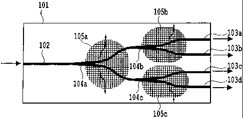
[ 0044 ] Fig. 5 shows a removing method of the leakage
light in the optical branching circuit . A 1 x 4 optical
branching circuit is composed of a waveguide type
branching circuit on a substrate 101. Then, the light
made incident from an input waveguide 102 is transmitted
through three branching waveguides 104a to 104c and
emitted from four output waveguides 103a to 103d. At
this time, the axis displacement and mode mismatch of
the optical fiber, which is optically coupled to an
input/output waveguide, cause the leakage light to be
generated inside the 1 x 4 optical branching circuit 101 .
Also, a radiation light or evanescent light generated
in the branching waveguide 104a becomes the leakage light
and is re-coupled to the branching wave guides 104b and
104c and the output waveguides 103a to 103d, and then
deteriorates the uniformity of the output power of the
branch light. Similarly, the radiation lights or
evanescent lights generated in the branching waveguides
104b and 104c become the leakage lights and are re-coupled
CA 02552417 2006-06-30
- 25 -
to the output wave guides 103a to 103d, and then deteriorate
the uniformity of the output power of the branch light .
[0045] Therefore, in order to prevent the leakage
lights generated in the branching waveguides 104a to 104c
from being re-coupled to the waveguides, stray light
guides 105a to 105c are installed. The stray light guides
105a to 105c are the above-mentioned wave propagation
mediums and arranged in the finite regions of the clad
portion in the substrate 101. The leakage lights
generated in the branching waveguides 104a to 104c are
emitted to the side, in which the input/output waveguides
of the substrate 101 are not formed, by the stray light
guides 105a to 105c.
[0046] Fig. 6 shows an insertion loss of the 1 x 4
optical branching circuit. Thisshowsthe insertion loss
between the input waveguide and each output waveguide ,
when the light of a wavelength 1 . 55 ~.m is made incident .
The variation in the insertion loss when the stray light
guides 105a to 105c are present is 0 . 1 dB, and the variation
in the insertion loss when there is no stray light guide
is 1 dB . It is found that the leakage light is removed
by the stray light guide using the wave propagation medium .
Second Embodiment
[0047] Fig. 7 shows a removing method of a leakage
lightinthe MZ-type opticalcombining/splitting circuit.
The MZ-type optical combining/splitting circuit is
' CA 02552417 2006-06-30
- 26 -
provided with an optical coupler 114a coupled to input
waveguides 112a and 112b, an optical coupler 114b coupled
to output waveguides 113a and 113b, and arm waveguides
116a and 116b for coupling the optical coupler 114a and
the optical coupler 114b. Similarly to the first
embodiment , the axis displacement and mode mismatch of
the optical fibers optically coupled to the input/output
waveguides cause the leakage light to be generated inside
the MZ-type optical combining/splitting circuit. Also,
the radiation lights or evanescent lights generated in
the optical couplers 114a and 114b become the leakage
lights and are re-coupled to the arm waveguides 116a and
116b and the output waveguides 113a and 113b, and then
deteriorate the crosstalk.
[0048] Therefore, in order to prevent the leakage
lights generated in the optical coupler 114a and 114b
from being re-coupled to the optical waveguides , stray
light guides 115a and 115b are installed. The stray light
guides 115a and 115b are the above-mentioned wave
propagation mediums and arranged in the finite regions
of the clad portion in a substrate 111. The leakage lights
generated in the optical couplers 114a and 114b are emitted
to the side, in which the input/output wave guides of the
substrate 111 are not formed, by the stray light guides
115a and 115b.
[ 0049 ] Figs . 8A and 8B show the transmission spectrum
of the MZ-type optical combining/splitting circuit . Fig.
' CA 02552417 2006-06-30
r ~ ~ I
- 27 -
8A shows the transmission spectrum of the MZ-type optical
combining/splitting circuit without any stray light
guide, and the crosstalk is 25 dB. Fig. 8B shows the
transmission spectrum of the MZ-type optical
combining/splitting circuit to which the removing method
of the leakage light according to the second embodiment
is applied, and the crosstalk is 40 dB. It is found that
the leakage light is removed by the stray light guides
115a and 115b using the wave propagation medium.
[ 0050 ] In the first and second embodiments , since the
holographic wave propagation medium is applied as the
optical part for removing the leakage light, in the
conventional optical circuit, it is possible to attain
an optical functional circuit having excellent circuit
property where the interference is not generated between
the plurality of output ports, and the transmission loss
and the crosstalk are small.
Third Embodiment
[0051] With reference to the transmission spectrum
of the optical combining/splitting circuit shown in Fig.
4, it is found that a part of the transmission light to
be emitted to an output port b is emitted to an output
port a. This is because with a manufacturing error when
the wave propagation medium having the shape of the mesh
is manufactured, a part of the light to be transmitted
through the wave propagation medium is not outputted to
~
CA 02552417 2006-06-30
_ 2g _
a predetermined output port but emitted to a different
output port or leaked from the portion other than the
output port . In this way, among the light signals made
incident from the input port , the light that is not emitted
from the predetermined output port, namely; the
transmission light that does not contribute to the circuit
operation assumed on the design or obstructs the circuit
operation is hereinafter referred to as "stray light . "
As shown in Fig. 4, it is found that the transmission
light to be emitted to the output port b is emitted as
the stray light to the output port a.
[ 0052 ] The removing method of this stray light will
be described below in detail by exemplifying the optical
combining/splitting circuit shown in Fig. 3. Fig. 9
shows the removing method of the stray light according.
to the third embodiment of the present invention . With
respect to an optical axis 3-11 on an input port 3-1 in
the optical combining/splitting circuit, optical axes'
3-12a and b of an output port 3-2 are shifted in a lateral
directiononacoordinateX. Specifically with reference
to Fig . 9 , it is assumed to be a half value 8 of a beam
divergence angle of the incident light from the input
port 3-1. The output port 3-2 may be arranged outside
the intersection of the exit facet 2-2 and two lines of
an angle 8 from the input port 3-1 with respect to the
optical axis 3-11 of the input port 3-1.
[0053] That is, the transmission light components
' CA 02552417 2006-06-30
- 29 -
that do not contribute to the circuit operation assumed
on the design are scattered by the pixels whose refractive
indexes are different. However, the whole thereof is
substantially straightly advanced. Thus, only by
shifting and setting the optical axes 3-12a and b of the
output port 3-2 with respect to the optical axis 3-11
of the input port 3-1, there is a certain effect of removing
the stray light.
[ 0054 ] Fig. 10 shows the transmission spectrum of the
optical combining/splitting circuit according to the
third embodiment. As compared with the spectrum shown
in Fig. 4, it is found that the stray light that has been
emitted to the output port a is suppressed. In this way,
by application of the holographic wave propagation medium,
miniaturization can be attained and it is possible to
attain the optical functional circuit having the
excellent circuit property where the interference is not
generated between the plurality of output ports , and the
transmission loss and the crosstalk are small.
Fourth Embodiment
[ 0055 ] Fig. 11 shows a removing method of the stray
light according to the fourth embodiment of the present
invention. Similarly to the third embodiment, the
optical axes 3-12a and b of the output port 3-2 are shifted
with respect to the optical axis 3-11 of the input port
3-1. In the fourth embodiment, the output port 3-2 is
' CA 02552417 2006-06-30
- 30 -
set for an exit facet 2-3 on x=xe, and an angle between
the optical axis 3-11 and the optical axes 3-12a and b
are square.
[0056] At this time, the calculation for calculating
the refractive index distribution may be calculated along
the straight line to connect the input port 3-1 and the
output port 3-2. In this case, the input field and the
output field are inclined and given.
Fifth Embodiment
[ 0057 ] Fig. 12 shows a removing method of the stray
light according to the fifth embodiment of the present
invention. In addition to the configuration of the
fourth embodiment, a stray light guide 4 is arranged.
In the fourth embodiment, along the optical axis 3-11
of the input port, the stray light is considered to be
outputted in the direction of the exit facet 2-2.
Therefore, the stray light guide 4 is arranged such that
the stray lights around the optical axis 3-11 can be
collected and collectively outputted to the left end of
the exit facet 2-2.
[0058] In the calculation for calculating the
refractive index distribution of the stray light guide
4 , the input end facet of the stray light guide is suitably
determined to determine the stray light field on the input
end facet . Next , along the axis based on the input end
facet , the calculation is carried out in accordance with
CA 02552417 2006-06-30
~ ' ~ I
- 31 -
the above-mentioned algorithm.
Sixth Embodiment
[ 0059 ] Fig. 13 shows a removing method of the stray
light according to the sixth embodiment of the present
invention. In addition to the configuration of the third
embodiment , an input waveguide 5 -1 and output waveguides
5-2a and b are arranged. In the optical circuit shown
in Fig . 9 , the input port 3 -1 and output port 3 - 2 of the
wave propagation medium formed insidethe optical circuit
design region 1-1 do not have any structural boundary.
Thus, the connection to the optical fiber is difficult.
[0060] Therefore; the waveguide 5-1 connected to the
input port and the waveguides 5-2a and b connected to
the output port are formed on a substrate 1-2 around the
optical circuit design region 1-1. The optical
waveguides 5-1 and 5-2 are the straight waveguides
composed of core portions and clad portions around the
core portions and have the structural boundaries. Thus,
the connections to optical fibers 6-1 and 6-2 are easy.
[ 0061 ] It is noted that , in the sixth embodiment , the
straight waveguide is described, however, the optical
waveguide has flexibility in layout, and a curved
waveguide is also possible . Thus , the degree of freedom
of the positional relationship between the input port
and the output port of the optical circuit design region
1-1 and the optical fiber is increased.
, ' CA 02552417 2006-06-30
- 32 -
Seventh Embodiment
[ 0062 ] Fig. 14 shows a removing method of the stray
light according to the seventh embodiment of the present
invention . The seventh embodiment is one example of the
complex optical circuit having a plurality of optical
circuit design regions on which the wave propagation
mediums designed by the design procedure shown in Fig.
2 are formed. An optical fiber 6-1 is optically coupled
to the input waveguide 5-1 connected to the input port
of an optical circuit design region 1-1a. The optical
circuit design region 1-1a is, for example, the optical
combining/splitting circuit and has two output ports.
The output ports are connected via connection waveguides
5-3a and b to the input ports of an optical circuit design
region 1-1b, respectively. The optical circuit design
region 1-lb is, for example, a filter circuit and has
two output ports . The output ports are optically coupled
via output waveguides 5-2a and b to optical fibers 6-2a
and b, respectively.
[0063] In the optical circuit design region 1-1a, as
described in the third embodiment , with respect to the
optical axis of the input port , the optical axis of the
output port is shifted laterally on the coordinate x.
Around the input waveguide 5-1, similarly to the fifth
embodiment, a stray light guide 4-2 is arranged such that
the stray light generated in the connection portion
' CA 02552417 2006-06-30
- 33 -
between the optical fiber and the input waveguide is not
inputted to the optical circuit design region 1-1a.
[ 0064 ] Also, around the waveguides 5-3a and b, a stray
light guide 4-3 is arranged such that the stray light
generated in the connection portion between the output
port and the waveguide is not inputted to the optical
circuit design region 1-1b. Also around the output
waveguides 5-2a and b, stray light guides 4-4a and b are
arranged such that the stray light generated in the
connection portion between the output port and the
waveguide is not coupled to the optical fibers.
[ 0065 ] In this way, so as to prevent the stray light
generated in the connection portion and the stray light
generated in the wave propagation medium from being
inputted to the optical circuit at the next stage, it
is possible to constitute the optical circuits each having
the excellent circuit property. Also, by application
of the holographic wave propagation medium,
miniaturization of the optical circuit can be attained.
[0066] In the third to seventh embodiments, by
application of the holographic wave propagation medium,
miniaturization of the optical circuit is attained.
Moreover,-the optical axis of the input port and the
optical axis of the output port are arranged so as not
to be made coincident with each other. Consequently,
it is possible to attain the optical functional circuit
having the excellent circuit property where the
CA 02552417 2006-06-30
- 34 -
interference is not generated between a plurality of
output ports, and the transmission loss and the crosstalk
are small.
Eighth Embodiment
[0067] As mentioned above, the axis displacement and
mode mismatch of the optical fiber optically coupled to
the input/output waveguide cause the generation of the
leakage light and the generation of the stray light.
Therefore, connection of the optical waveguide device
to which the holographic wave propagation medium is
applied is made easier to attain the optical functional
circuit where the transmission loss and the crosstalk
are small.
[ 0068 ] Fig. 15 shows the configuration of an optical
waveguide device including . an optical
combining/splitting circuit according to the eighth
embodiment of the present invention. The optical
waveguide device is constituted by connecting the optical
fiber to the optical combining/splitting circuit shown
in Fig . 3 and enclosing in a package ( not shown ) . The
optical fibers 13a to 13c are coupled to an input port
on the incidence facet of a wave propagation medium 11
formed on a substrate 10 and the output ports on the exit
facet . The optical fibers 13a to 13c are fixed to fixing
glass blocks 12a to 12c and coupled to the input and output
ports while alignment between the substrate 10 and the
CA 02552417 2006-06-30
~ . I
- 35 -
glass blocks 12a to 12c is performed.
[ 0069 ] The wave propagation medium 11 does not have
the structural boundary because of the mesh-shaped pixel .
Thus , it is difficult to visually discriminate the light
focusing positions of the input and output ports.
Therefore, on the substrate 10, positioning markers 15a
to 15c are formed with reference to the coordinates of
the input and output ports determined at the time of the
calculation. As for the positioning markers 15a to 15c,
a waveguide core may be formed on the substrate 10 , or
a metal may be formed on the surface of the substrate
10. The alignment can be easily performed by forming
the markers corresponding to the light focusing positions
of optical fibers 23a to 23c even on the opposite glass
blocks 12a to 12c.
Ninth Embodiment
[ 0070 ] Fig. 16 shows the configuration of an optical
waveguide device including an optical
combining/splitting circuit according to the ninth
embodiment of the present invention. In the region where
the beam diameter of the light near the input and output
ports is small, it is necessary to reduce the rate of
the component that is obliquely incident with respect
to the propagation direction of the light and consequently
suppress the crosstalk. Therefore, a waveguide 25a is
connected to an input port of a wave propagation medium
' CA 02552417 2006-06-30
- 36 -
21 serving as the optical combining/splitting circuit
shown in Fig. 3. Then, optical waveguides 25b and 25c
are connected to output ports . Moreover, on a substrate
20, wave propagation mediums 24a to 24c for mode field
conversion are formed, thereby improving the coupling
efficiency between the optical waveguides 25a to 25c and
optical fibers 23a to 23c.
[ 0071 ] Positioning markers 26a to 26c are used even
in the connection between the optical fibers 23a to 23c
and the wave propagation mediums 24a to 24c for mode field
conversion. That is, on the substrate 20, the
positioning markers 26a to 26c are formed with reference
to the coordinates of the input and output ports determined
at the time of the calculation, and the markers
corresponding to the light focusing positions of the
optical fibers 23a to 23c are formed even on the opposite
glass blocks 22a and 22b. Consequently, alignment can
be easily performed.
Tenth Embodiment
[ 0072 ] Fig. 17 shows the configuration of an optical
wavegulde device including an optical
combining/splitting circuit according to the tenth
embodiment of the present invention . The difference from
the ninth embodiment lies in the difference in the
configuration of the wave propagation mediums 24a to 24c
for mode field conversion.
' CA 02552417 2006-06-30
- 37 -
[ 0073 ] In the wave propagation mediums 24a to 24c in
the ninth embodiment, the entire refractive index
distribution of the wave propagation mediums is
determined in accordance with the refractive indexes
(here, the binary refractive indexes) possessed by the
respective virtual pixels defined by the virtual mesh.
In the tenth embodiment, the typical algorithm for
determining the above-mentionedspatial refractive index
distribution is used to determine the refractive index
distribution by modulating a core width of the optical
waveguide in an optical axis direction, as shown in Fig.
17.
[ 0074 ] The configuring method of the width of the core
of the wave propagation medium 24a is simply explained.
1f When the refractive index distribution is given which
minimizes the phase difference between the field of the
signal light inputted from the optical fiber 23a and the
field where the field in which the phase of the field
of the desirable signal light to be outputted to the wave
propagation medium 21 is inverted is propagated to the
optical fiber 23a, the inputted signal light can be
converted into the desirable output signal light.
Specifically, the phase difference between the
respective positions in the optical axis direction is
calculated. Then, if the phase difference is positive,
the core width of the optical waveguide is increased,
and if the phase difference is negative, the core width
CA 02552417 2006-06-30
- 38 -
of the optical waveguide is decreased. Consequently,
the phase difference is minimized. In accordance with
such a configuring method, the width of the core of the
optical waveguide which minimizes the phase difference
is determined by each calculation. Thus, the inputted
signal light can be converted into the desirable output
signal light.
Eleventh Embodiment
[ 0075 ] Fig. 18 shows the configuration of an optical
waveguide device including an optical
combining/splitting circuit according to the eleventh
embodiment of the present invention. The substrate 20,
on which the wave propagation medium 21 serving as the
optical combining/splitting circuit shown in Fig. 3 is
formed, and a substrate 40, on which a light emitting
element 41 and a light receiving element 42 are placed,
are coupled and enclosed in a package (not shown).
Consequently, the optical waveguide device is
constituted. Optical waveguides 25b and 25c are
connected to the output ports of the wave propagation
medium 21, and wave propagation mediums 27a and 27b serving
as light collecting lenses are formed, thereby improving
the coupling efficiency to the light emitting element
41 and the light receiving element 42.
[0076] Even for the connection between the wave
propagation mediums 27a and 27b serving as the light
CA 02552417 2006-06-30
~ ' ~ I
- 39 -
collecting lenses and the light emitting element 41 and
the light receiving element 42, positioning markers 26b
and 26c are used. In this way, since the light collecting
lenses are formed as the wave propagation mediums on the
substrate, the optical waveguide device can be
miniaturized. Conventionally, when the optical
waveguide device is manufactured, the optical axis
alignment is required among the light emitting element
and the light receiving element, the light collecting
lens, and the optical combining/splitting device.
However, according to this embodiment , only the alignment
by the positioning markers is performed, which can reduce
the manufacturing step of the optical waveguide device.
Twelfth Embodiment
[ 0077 ] Fig. 19 shows the configuration of an optical
waveguide device including an optical
combining/splitting circuit according to the twelfth
embodiment of the present invention. The substrate 20,
on which the wave propagation medium 21 serving as the
optical combining/splitting circuit shown in Fig. 3 is
formed, and a substrate 50, for example, on which an
optical switch 51 and an optical filter 52 are formed,
are coupled and enclosed in a package (not shown).
Consequently, the optical waveguide device is
constituted. The optical wave guides 25b and 25c of the
substrate 20 and the optical waveguide of the substrate
CA 02552417 2006-06-30
- 40 -
50 are connected by the wave propagation mediums 24b and
24c for mode field conversion.
[0078] For the alignment for the connection,
similarly to the case of the optical fiber in Fig. 16,
the positioning markers 26b and 26c are used. In this
way, even the connection between a conventional PLC
circuit and the wave propagation medium can be easily
performed by using the positioning marker. According
to the eighth and ninth embodiments and this embodiment,
the optical waveguide devices of the various
configurations can be easily combined.
Thirteenth Embodiment
[ 0079 ] Fig. 20 shows the configuration of an optical
waveguide device. including an optical
combining/splitting circuit according to the thirteenth
embodiment of the present invention. A waveguide 35a
is connected to an input port of a wave propagation medium
31 on a substrate 30, and optical waveguides 35b and 35c
are connected to an output port . Similarly to the ninth
embodiment, wave propagation mediums 34a to 34c for mode
field conversion are further formed, thereby improving
the coupling efficiency between the optical waveguides
35a to 35c and optical fibers 33a and 33b for input and
output.
[0080] The connection between the wave propagation
r mediums 34a to 34c for mode field conversion and the
' CA 02552417 2006-06-30
- 41 -
optical f fibers 33a and 33b for input and output , monitoring
wave guides 36a and 36b are used. That is , on the substrate
30, ports of the monitoring waveguides 36a and 36b are
formed with reference to the coordinate of the input and
output ports determined at the time of the calculation.
Then, the optical fibers 33a and 33b for positioning,
which correspond to the light focusing positions of the
optical fibers , are held even for opposite glass blocks
32a and 32b. A light source and an optical power meter
are connected via the optical fibers 33a and 33b for
positioning and the monitoring waveguides 36a and 36b.
Then, while the optical intensities are measured, the
connection positions are determined. Thus, it is
possible to easily perform the alignment between the wave
propagation mediums 34a to 34c for mode field conversion
and the optical fibers 33a and 33b for input and output .
Fourteenth Embodiment
[ 0081 ] Fig. 21 shows the configuration of an optical
waveguide device including an optical
combining/splitting circuit according to the fourteenth
embodiment of the present invention . The difference from
the thirteenth embodiment lies in the structure that the
wave propagation mediums 34a to 34c for mode field
conversion are the wave propagation mediums in which the
waveguide widths are modulated, similarly to the tenth
embodiment.
~ CA 02552417 2006-06-30
. ' ,
- 42 -
[0082] According to the eighth to fourteenth
embodiments, by using the positioning markers or
monitoring waveguides formed on the substrate, the
optical waveguide device to which the holographic wave
propagation medium is applied can be easily connected.
Fifteenth Embodiment
[ 0083 ] Fig . 22 shows the configuration of an optical
network unit (ONU) according to the fifteenth embodiment
of the present invention. The ONU is the apparatus
installed in a subscriber house in an optical fiber
subscriber network, and the optical signal is transmitted
to and received from an optical line terminal (OLT) on
a station side. A wavelength of 1.55 ~.m is used in a
descending signal of OLT-ONU, and a wavelength of 1.55
~,m is used in an ascending signal of the OLT-ONU.
[ 0084 ] The ONU is provided with a PD202 for receiving
the descending signal, an LD203 for transmitting the
ascending signal, a monitor PD204 for monitoring a power
of an output light of the LD203, and a WDM filter 205
for combining and splitting the ascending signal and the
descending signal, on a PLC substrate 201. Also, the
signal which is wavelength-multiplexed by the WDM filter
205 is connected to the OLT via an optical fiber 207 fixed
to a glass block 206. In the ONU, the leakage light is
generated in the connection portions between the PD202
and the optical waveguide, between the LD203 and the
' CA 02552417 2006-06-30
~ I
- 43 -
optical waveguide, between the WDM filter 205 and the
optical waveguide, and between the optical fiber 207 and
the optical waveguide.
[ 0085 ] Therefore, the removing method of the leakage
light described in the above-mentioned embodiments and
the like are applied. The wave propagation mediums 211
and 212 have the function of the light collecting lens ,
as described in the eleventh embodiment and improve the
coupling efficiencies between the PD202 and the optical
waveguide and between the LD203 and the optical waveguide,
respectively. At the intersection portion of the WDM
filter and the optical waveguide, as described in the
first and second embodiments, the stray light guides 213a
and 213b constituted by the wave propagation mediums are
installed, thereby preventing the leakage light from
being again coupled to the optical waveguide. Moreover,
as described in the eighth embodiment , the markers 215a
and 215b are used for the connection between the PLC
substrate 201 and the glass block 206. As described in
the ninth embodiment, the wave propagation medium 21 for
mode field conversion is used for the coupling between
the optical fiber 207 and the optical waveguide.
[0086] In this way, by improving the coupling
efficiency of the optical coupling at each connection
portion and further suppressing the crosstalk, it is
possible to avoid the deterioration in S/N as an optical
receiver. Also, the connection at the mounting step is
CA 02552417 2006-06-30
- 44 -
made easier, which can reduce the number of the mounting
steps and consequently improve the productivity.