Language selection

Search

Patent 2552543 Summary

Third-party information liability

Some of the information on this Web page has been provided by external sources. The Government of Canada is not responsible for the accuracy, reliability or currency of the information supplied by external sources. Users wishing to rely upon this information should consult directly with the source of the information. Content provided by external sources is not subject to official languages, privacy and accessibility requirements.

Claims and Abstract availability

Any discrepancies in the text and image of the Claims and Abstract are due to differing posting times. Text of the Claims and Abstract are posted:

  • At the time the application is open to public inspection;
  • At the time of issue of the patent (grant).
(12) Patent: (11) CA 2552543
(54) English Title: SWITCHING DEVICE PROVIDED WITH NEUTRAL CONDUCTOR
(54) French Title: DISPOSITIF DE COMMUTATION DOTE D'UN CONDUCTEUR NEUTRE
Status: Expired and beyond the Period of Reversal
Bibliographic Data
(51) International Patent Classification (IPC):
  • H1H 71/00 (2006.01)
  • H1H 3/54 (2006.01)
(72) Inventors :
  • MATTLAR, HARRI (Finland)
  • KOLMONEN, RAINER (Finland)
  • SUUTARINEN, AKI (Finland)
(73) Owners :
  • ABB OY
(71) Applicants :
  • ABB OY (Finland)
(74) Agent: GOWLING WLG (CANADA) LLP
(74) Associate agent:
(45) Issued: 2013-07-02
(86) PCT Filing Date: 2005-01-18
(87) Open to Public Inspection: 2005-07-28
Examination requested: 2009-11-19
Availability of licence: N/A
Dedicated to the Public: N/A
(25) Language of filing: English

Patent Cooperation Treaty (PCT): Yes
(86) PCT Filing Number: PCT/FI2005/000030
(87) International Publication Number: FI2005000030
(85) National Entry: 2006-07-05

(30) Application Priority Data:
Application No. Country/Territory Date
20040072 (Finland) 2004-01-19

Abstracts

English Abstract


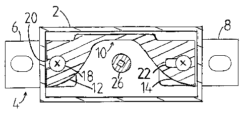
A switching device provided with a neutral conductor and arranged for opening
and closing an electric circuit, the switching device comprising a frame (2),
through which the electric circuit's neutral conductor (4) having a first end
(6) and a second end (8) passes. The neutral conductor (4) comprises a movable
middle portion (10) that is arranged for breaking the neutral conductor (4)
inside the frame (2), the movable middle portion (10) being movable with
respect to the first (6) and the second (8) end of the neutral conductor (4)
and located between them.


French Abstract

La présente invention concerne un dispositif de commutation doté d'un conducteur neutre et conçu pour ouvrir et fermer un circuit électrique, ce dispositif de commutation comprenant un bâti (2) à travers lequel passe le conducteur neutre du circuit électrique (4) qui présente une première extrémité (6) et une seconde extrémité (8). Le conducteur neutre (4) comporte une partie médiane mobile (10) qui est conçue pour rompre le conducteur neutre (4) à l'intérieur du bâti (2), ladite portion médiane mobile (10) étant mobile par rapport à la première extrémité (6) et à la seconde extrémité (8) du conducteur neutre (4) et disposée entre ces deux extrémités.

Claims

Note: Claims are shown in the official language in which they were submitted.


6
WHAT IS CLAIMED IS:
1. A switching device provided with a neutral conductor and ar-
ranged for opening and closing an electric circuit, the switching device com-
prising a frame (2), through which the electric circuit's neutral conductor
(4)
having a first end (6) and a second end (8) passes, the neutral conductor (4)
comprising a movable middle portion (10) that is arranged for breaking the
neutral conductor (4) inside the frame (2), the movable middle portion (10) be-
ing movable with respect to the first (6) and the second (8) end of the
neutral
conductor (4) and located between them, the switching device comprising
pressing means (16) for pressing the movable middle portion (10) against the
first (6) and the second (8) end of the neutral conductor (4), the pressing
means (16) being adapted to selectively lock the movable middle portion (10)
in a broken position and in a contact position, the broken position being the
position where there is no electrically conductive connection between the
first
end (6) of the neutral conductor (4) and the second end (8) of the neutral con-
ductor (4), and the contact position being the position where the first end
(6) of
the neutral conductor (4) is in electrically conductive connection with the
sec-
ond end (8) of the neutral conductor (4), characterized in that the pressing
means (16) comprise one screw member (18) per each end of the movable
middle portion (10), each screw member (18) comprising a threaded portion
and a head portion and the diameter of the head portion being larger than that
of the threaded portion.
2. A switching device according to claim 1, characterized in that
the movable middle portion (10) comprises a slot (20, 22) at its first end
(12)
and at its second end (14), each slot (20, 22) forming an opening extending
through the middle portion (10), and that the threaded portions of the screw
members (18) are arranged to pass through the movable middle portion (10)
via the slots (20, 22).
3. A switching device according to claim 2, characterized in that
one end of the slot (20) at the first end (12) of the movable middle portion
(10)
is open.
4. A switching device according to claim 3, characterized in that
the slot (22) at the second end (14) of the movable middle portion (10) is so
long that the neutral conductor (4) can be broken by loosening the screw
members (18) and by sliding the movable middle portion (10) along the surface

7
of the first (6) and the second (8) end of the neutral conductor towards the
second end (8) of the neutral conductor until the movable middle portion (10)
reaches a position where it is not in a conductive contact with the first end
(6)
of the neutral conductor (4).
5. A switching device according to any one of claims 1 - 4, char-
acterized in that the movable middle portion (10) comprises a portion (24)
which is in a substantially perpendicular plane with respect to the plane in
which the first (12) and the second end (14) of the movable middle portion
(10)
are located.
6. A switching device according to any one of claims 1 - 5, char-
acterized in that the switching device is a modular switching device and that
the neutral conductor (4) is located in a control device module.

Description

Note: Descriptions are shown in the official language in which they were submitted.


CA 02552543 2006-07-05
WO 2005/069332 PCT/FI2005/000030
1
SWITCHING DEVICE PROVIDED WITH NEUTRAL CONDUCTOR
BACKGROUND OF THE INVENTION
[0001] The invention relates to a switching device provided with a
neutral conductor according to the preamble of the independent claim.
[0002] Switching devices are apparatuses that are used for opening
and closing an electric circuit. A switching device comprises at least one
pole
connected to a phase conductor and a control device for opening and closing
this pole. Examples of switching devices are switches and switch fuses.
[0003] It is known to arrange a neutral conductor to pass through a
switching device.
[0004] In some situations, for example when a switching device is
installed or serviced, it is necessary to perform measurements or tests where
the influence of the neutral conductor has been eliminated. Breaking the neu-
tral conductor may be required in connection with an insulation level meas-
urement, for instance. In prior art switching devices, however, the breaking
of a
neutral conductor is often difficult, or the structure of the breaking
mechanism
is complex.
BRIEF DESCRIPTION OF THE INVENTION
[0005] The object of the invention is to provide a switching device
provided with a neutral conductor to solve the above-mentioned problems. The
object of the invention is achieved by a switching device which is
characterized
by what is disclosed in the independent claim. Preferred embodiments of the
invention are disclosed in the dependent claims.
[0006] The invention is based on the neutral conductor comprising a
movable middle portion for breaking the neutral conductor.
[0007] An advantage of the switching device according to the inven-
tion is that the neutral conductor can be broken quickly and easily for meas-
urements or testing, for example. A 'further advantage is that the structure
of
the breaking mechanism is simple.
BRIEF DECRIPTION OF THE FIGURES
[0008] The invention will now be described in greater detail by
means of preferred embodiments, with reference to the accompanying draw-
ings, in which

CA 02552543 2006-07-05
WO 2005/069332 PCT/FI2005/000030
2
Figure 1 is a top view of a partly dismantled control device module
of a switching device according to an embodiment of the invention; and
Figure 2 is a cross-sectional side view of the control device module
of Figure 1.
DETAILED DESCRIPTION OF THE INVENTION
[0009] In the control device module of Figure 1, a neutral conductor
4, which is arranged to be broken, passes through a frame 2. The neutral con-
ductor 4 comprises a first end 6, a second end 8 and a movable middle portion
10.
[0010] The first end 6 of the neutral conductor 4 is close, to the first
side of the frame 2 and the second end 8 of the neutral conductor 4 is close
to
the second side of the frame 2. The first and the second side of the frame are
opposite to each other. The movable middle portion 10 of the neutral conductor
can be moved with respect to the first 6 and the second 8 end of the neutral
conductor 4, and it is located between them so that the first end 12 of the
mov-
able middle portion 10 is close to the first end 6 of the neutral conductor 4
and
the second end 14 of the movable middle portion 10 is close to the second end
8 of the neutral conductor 4.
[0011] Both the first 6 and the second 8 end of the neutral conduc-
for are formed of a substantially rectangular planar preform by bending it so
as
to provide it with a cross-sectional shape that resembles the letter U, where
one of the branches of the letter U is longer than the other. The longer
branch
extends outside the frame 2 and is arranged to be connected to the neutral
wire of the electric circuit or to another similar structure. The first 6 and
the
second 8 end are arranged so that the longer branch of the letter U is located
lower than the shorter branch.
[0012] The movable middle portion 10 of the neutral conductor is
formed of a planar preform by bending the middle portion of the preform so
that it is at a right-angle towards the rest of the preform. Thus the middle
por-
tion of the preform forms portion 24 which is at an angle of 90° with
respect to
the plane in which the first 12 and the second 14 end of the movable middle
portion 10 are located.
[0013] The portion 24 of the movable middle portion 10 is in a dif-
ferent plane than the ends of the middle portion 10 since a control shaft 26
of
the switching device passes in the middle of the frame 2, the control shaft be-

CA 02552543 2006-07-05
WO 2005/069332 PCT/FI2005/000030
3
ing arranged to control the switching device. The bent structure of the
movable
middle portion 10 thus improves space utilization inside the frame 2. In
addition
to the movable middle portion 10, attention is preferably paid to space
utiliza-
tion in the design of the first 6 and thesecond 8 end of the neutral conductor
4,
too, i.e. to the arrangement of other components inside the frame 2 as well as
to their easy installation. The components to be mounted inside the frame 2,
which are preferably taken into account in the shaping of the neutral
conductor
4, include auxiliary contacts and microswitches and the main shaft of the
switching device. These components are not shown in the figures.
[0014] The parts of the neutral conductor 4 are shaped to enable
the portion 24 to slide to the side of the second end 8 of the neutral
conductor,
whereby the portion 24 is partly between the second end 8 of the neutral con-
ductor and the frame 2 wall.
[0015] When the first end 6 of the neutral conductor 4 is desired to
be in contact with the second end 8 of the neutral conductor 4, the movable
middle portion 10 is pressed against the first 6 and the second end 8 by press-
ing means 16. The pressing means 16 comprise one screw member 18 per
each end of the movable middle portion 10. Each screw member 18 comprises
a threaded portion and a head portion, the diameter of the head portion being
larger than that of the threaded portion. The lower surfaces of the head por-
tions of the screw members 18 are arranged to press the movable middle por-
tion 10 against the first 6 and the second 8 end of the neutral conductor when
the screw members are tightened.
[0016] The materials of the neutral conductor 4 and pressing means
16 have been selected and dimensioned to correspond to the currents passing
in the neutral conductor.
[0017] In the structure illustrated in Figure 2, the counterparts for
the screw members 18 are integrated into the first 6 and the second 8 end of
the neutral conductor 4, i.e. the ends are provided with threads that are ar-
ranged to cooperate with the respective threaded portion of the screw member
18. Alternatively, separate nuts can be employed.
[0018] The movability of the middle portion 10 is achieved by two
slots. At the first end 12 of the movable middle portion 10, there is an open
slot
20, and at the second end 14 a closed slot 22. The open slot 20 has one open
end and one closed end. The both ends of the closed slot 22 are closed. The
slots 20 and 22 are arranged to receive the threaded portion of the respective

CA 02552543 2006-07-05
WO 2005/069332 PCT/FI2005/000030
4
screw member 18. Each slot forms an opening extending through the middle
portion 10 so that the threaded portion of the respective screw member 18 may
pass through the movable middle portion 10 via the slot. The threaded portion
of the screw member 18 can be slid through-the open end of the open slot 20,
whereas each closed end of the slots prevents sliding the threaded portion
therethrough.
[0019] The width of both the open slot 20 and the closed slot 22 is
slightly larger than the diameter of the respective screw member and smaller
than the diameter of the head portion. In the direction perpendicular to the
lon-
gitudinal axis of the screw member 18, the length of the slots 20 and 22 is
greater than the diameter of the screw member 18. The closed slot 22 is sub-
stantially longer than the open slot 20.
[0020] The first end 12 of the movable middle portion 10 is detach
able from the first end 6 of the neutral conductor without removing the respec
tive screw member 18. When the respective screw member 18 has been loos
ened by turning it a bit in the opening direction, the first end 12 of the
movable
middle portion 10 can be slid away from below the head of the screw member
18. The second end 14 of the movable middle portion 10 cannot be fully de
tached from the second end 8 of the neutral conductor without removing the'
respective screw member 18.
[0021] In a preferred embodiment of the invention, the closed slot
22 is made so long that the movable middle portion 10 can be slid, without re-
moving the respective screw member 18 of the closed slot 22, into a position
where the middle portion 10 is not in a conductive contact with the first end
6 of
the neutral conductor 4 even though the respective screw member 18 of the
closed slot 22 were retightened. The neutral conductor 4 is thus broken by
loosening the screw members 18 and by sliding the movable middle portion 10
along the upper surface of the first 6 and the second 8 end of the neutral con-
ductor towards the second end 8 of the neutral conductor. By tightening the
screw member 18 at the second end 8, the movable middle portion 10 can be
locked in a desired position, in which case it cannot accidentally move into a
conductive contact with the first end 6 of the neutral conductor. An advantage
of this embodiment is that the conductive contact between the ends 6 and 8 of
the neutral conductor 4 can be reliably maintained broken during measure-
ments or testing without having to detach any part of the neutral conductor 4
or
the pressing means 16 from the switching device. As a result, none of the
parts

CA 02552543 2006-07-05
WO 2005/069332 PCT/FI2005/000030
of the neutral conductor 4 or pressing means is at the risk of disappearing
dur-
ing the measurement or testing.
[0022] In an alternative embodiment, both ends of the movable
middle portion 10 comprise a slot having an open end. In that case, the slots
5 can be adapted such that the movable middle portion 10 can be detached from
the switching device after the screw members 18 have been loosened, i.e. nei-
ther of the screw member 18 needs to be completely removed for detaching
the movable middle portion 10.
[0023] In Figure 2, the dashed line illustrates a lid 28 that covers the
neutral conductor 4 during the normal use of the switching device. The lid 28
is
quickly detachable and attachable for easy access to the neutral conductor 4.
In an embodiment, the lid 28 is arranged to be openable without tools.
[0024] The switching device structure according to the invention,
which comprises a neutral conductor that can be broken, was described above
in connection with a modular switching device. It is clear that the structure
ac
cording to the invention is also applicable to switching devices where the con-
trol apparatus is mounted in the same frame part with the switch poles.
[0025] It is obvious to a person skilled in the art that the inventive
concept can be implemented in various ways. The invention and its embodi
ments are thus not limited to the above examples but they may vary within the
scope of the claims.

Representative Drawing
A single figure which represents the drawing illustrating the invention.
Administrative Status

2024-08-01:As part of the Next Generation Patents (NGP) transition, the Canadian Patents Database (CPD) now contains a more detailed Event History, which replicates the Event Log of our new back-office solution.

Please note that "Inactive:" events refers to events no longer in use in our new back-office solution.

For a clearer understanding of the status of the application/patent presented on this page, the site Disclaimer , as well as the definitions for Patent , Event History , Maintenance Fee  and Payment History  should be consulted.

Event History

Description Date
Time Limit for Reversal Expired 2019-01-18
Letter Sent 2018-01-18
Change of Address or Method of Correspondence Request Received 2018-01-10
Grant by Issuance 2013-07-02
Inactive: Cover page published 2013-07-01
Inactive: Final fee received 2013-04-22
Pre-grant 2013-04-22
Notice of Allowance is Issued 2013-04-05
Letter Sent 2013-04-05
4 2013-04-05
Notice of Allowance is Issued 2013-04-05
Inactive: Approved for allowance (AFA) 2013-04-03
Amendment Received - Voluntary Amendment 2012-10-01
Inactive: S.30(2) Rules - Examiner requisition 2012-04-13
Amendment Received - Voluntary Amendment 2011-08-22
Inactive: S.30(2) Rules - Examiner requisition 2011-02-24
Letter Sent 2010-01-08
Request for Examination Received 2009-11-19
Request for Examination Requirements Determined Compliant 2009-11-19
All Requirements for Examination Determined Compliant 2009-11-19
Amendment Received - Voluntary Amendment 2009-11-19
Letter Sent 2006-10-12
Inactive: Correspondence - Transfer 2006-09-18
Inactive: Courtesy letter - Evidence 2006-09-12
Inactive: Cover page published 2006-09-12
Inactive: Single transfer 2006-09-08
Inactive: Notice - National entry - No RFE 2006-09-06
Application Received - PCT 2006-08-15
National Entry Requirements Determined Compliant 2006-07-05
Application Published (Open to Public Inspection) 2005-07-28

Abandonment History

There is no abandonment history.

Maintenance Fee

The last payment was received on 2012-12-20

Note : If the full payment has not been received on or before the date indicated, a further fee may be required which may be one of the following

  • the reinstatement fee;
  • the late payment fee; or
  • additional fee to reverse deemed expiry.

Patent fees are adjusted on the 1st of January every year. The amounts above are the current amounts if received by December 31 of the current year.
Please refer to the CIPO Patent Fees web page to see all current fee amounts.

Owners on Record

Note: Records showing the ownership history in alphabetical order.

Current Owners on Record
ABB OY
Past Owners on Record
AKI SUUTARINEN
HARRI MATTLAR
RAINER KOLMONEN
Past Owners that do not appear in the "Owners on Record" listing will appear in other documentation within the application.
Documents

To view selected files, please enter reCAPTCHA code :


To view images, click a link in the Document Description column (Temporarily unavailable). To download the documents, select one or more checkboxes in the first column and then click the "Download Selected in PDF format (Zip Archive)" or the "Download Selected as Single PDF" button.

List of published and non-published patent-specific documents on the CPD .

If you have any difficulty accessing content, you can call the Client Service Centre at 1-866-997-1936 or send them an e-mail at CIPO Client Service Centre.


Document
Description 
Date
(yyyy-mm-dd) 
Number of pages   Size of Image (KB) 
Description 2006-07-04 5 275
Drawings 2006-07-04 1 27
Claims 2006-07-04 2 71
Abstract 2006-07-04 2 88
Representative drawing 2006-09-10 1 12
Cover Page 2006-09-11 1 43
Claims 2011-08-21 2 76
Claims 2012-09-30 2 74
Cover Page 2013-06-11 1 43
Notice of National Entry 2006-09-05 1 193
Reminder of maintenance fee due 2006-09-18 1 110
Courtesy - Certificate of registration (related document(s)) 2006-10-11 1 105
Reminder - Request for Examination 2009-09-20 1 117
Acknowledgement of Request for Examination 2010-01-07 1 188
Commissioner's Notice - Application Found Allowable 2013-04-04 1 164
Maintenance Fee Notice 2018-02-28 1 178
PCT 2006-07-04 5 154
Correspondence 2006-09-05 1 27
Correspondence 2013-04-21 2 53