Note: Descriptions are shown in the official language in which they were submitted.
CA 02552731 2006-07-05
WO 2005/069777 PCT/US2004/041379
MICROLENS ARRAYS
CROSS-REFERENCE TO RELATED APPLICATIONS
This application is a continuation-in-part of U.S. Application No. 10/754,365,
entitled "Method for Making Micro-Lens Array" and filed January 8, 2004, which
is
incorporated herein by reference in its entirety.
TECHNICAL FIELD
This invention relates generally to optics and optical devices and more
particularly
to microlens arrays, methods for making microlens arrays, and microlens array
systems and
applications.
BACKGROUND
Microlens arrays provide optical versatility in a miniature package for
imaging
applications. Traditionally, a microlens is defined as a lens with a diameter
less than one
millimeter; however, a lens having a diameter as large as five millimeters or
more has
sometimes also been considered a microlens.
There are many conventional methods for manufacturing microlenses. For
example,
one commonly used technique for manufacturing microlenses begins by coating a
substrate
with a selected photoresist, exposing the photoresist coated substrate to
radiation through a
mask, or alternatively, subjecting the photoresist to gray scale laser
exposure. Upon heating
the substrate, the exposed photoresist melts and surface tension pulls the
material into the
form of convex lenses. The depth of the photoresist determines the focal
length of the lens.
Another method for the manufacture of microlenses is to use ion exchange. In
this
method, ions are diffused into a glass rod to give a radial refractive index
distribution. The
index of refraction is highest in the center of the lens and decreases
quadratically as a
function of radial distance from the central axis. Microlenses made using the
ion exchange
method are used to collimate light from fibers as, for example, in
telecommunication
applications.
In general for many applications, microlens arrays are preferred over discrete
microlenses. As an example, one manufacturing process for the production of
glass
microlens arrays generally involves reactive ion etching (RIE) of fused
silica. In general, it
CA 02552731 2006-07-05
WO 2005/069777 PCT/US2004/041379
is very difficult to meet all the requirements of microlens arrays using RIE.
The RIE
technology involves many steps before the final product can be produced and
thus the yield
is typically poor and the products are costly.
As another example, compression molding of optical quality glass to form
microlens arrays is also well known. This method includes compressing optical
element
preforms, generally known as gobs, at high temperatures to form a glass lens
element. In
the compression molding process, a gob is inserted into a mold cavity. The
mold resides
within an oxygen-free chamber during the molding process. The gob is generally
placed on
the lower mold and heated above the glass transition temperature and near the
glass
softening point. The upper mold is then brought in contact with the gob and
pressure is
applied to conform the gob to the shape of the mold cavity. After cooling, the
lens is
removed from the mold.
Unfortunately, compression molding an array of microlenses using one or more
preforms is subject to many difficulties, which may include alignment of
mechanical and
optical axes of each lens element with respect to a common axis and location
of each lens
element with respect to a reference point in the array. Furthermore, it is
extremely difficult
to machine convex aspheric mold cavities using conventional techniques if the
microlens
diameter is less than 1 mm.
As another example, microlens arrays are often formed on the top surface of
silicon
chips, either for light-sensitive (e.g., CCDs) or light-emitting (e.g., micro-
display devices)
applications. A planarization layer is first formed over the silicon
substrate. A color filter
layer is next formed over the planarization layer with sub-pixel areas
properly aligned with
active devices in the silicon substrate. Another planarization layer is
generally formed over
the color filter layer and, finally a photoresist material is deposited over
the second
planarization layer. Conventional lithographic techniques are then utilized to
form
rectangular patterns in the photoresist. After exposure, a development step
removes the
photoresist in the exposed areas leaving the central island regions over the
pixel-active
areas transparent. Development and sometimes etching, removes the photoresist
material
between these central regions and forms trenches in the photoresist area
separating the
islands of photoresist now defining the individual microlens sites. A deep
plasma etch into
the silicon substrate next removes all layers above the substrate. Photoresist
is then stripped
and the devices are hard-baked to reflow the micro lenses into the proper
optical form by
controlling time and temperature.
2
CA 02552731 2006-07-05
WO 2005/069777 PCT/US2004/041379
Although there are many conventional methods for producing microlenses and
microlens arrays, these conventional techniques may involve difficult or
expensive
manufacturing steps or fail to meet certain design requirements, such as for
example in
terms of viewing angle, brightness, uniformity, or contrast. Consequently,
there is a need
for an improved microlens array.
SUMMARY
Systems and methods are disclosed herein to provide microlens arrays. For
example,
in accordance with an embodiment of the present invention, a method for
manufacturing a
microlens array is disclosed. The microlens array may be manufactured without
requiring
difficult or expensive manufacturing steps as required by some conventional
microlens
arrays. The microlens array may also meet the design requirements for a
display screen,
such as for example in terms of brightness and uniformity, contrast, and/or
viewing angle.
For example, the microlens array may be utilized as a television screen, a
computer screen
(e.g., computer monitor), a photocopy screen, a projection screen, a display
screen (e.g.,
ranging from a cellular phone display screen to a wall-sized display screen),
a laptop
screen, or with various other types of imaging, optical, or display systems.
In accordance with an embodiment of the present invention, for example, a
method
is provided for manufacturing a microlens array. The method includes adhering
or binding
together a bundle of optically transparent members, such as rods or fibers.
The bundle of
optically transparent members is cut to form sheets of member segments. The
cross-section
or faces of the sheet may resemble a honeycomb-like structure. The faces may
be polished
to smooth out any rough edges created by the cutting process. If desired, one
or both faces
or ends of the sheets can be modified to shape the ends into a desired shape.
The modified ends are exposed to an energy source, such as a heat source,
electrical
spike, laser light and the like, which causes the end of each member segment
to form a lens
segment. A light-shielding layer may be placed over the modified ends on one
side or both
sides of the sheet, leaving, for example, the lens segment of each member
segment only
partially exposed (e.g., only a central portion of each lens segment allowing
light through).
One or more coatings may be applied on both sides or on only one side of the
sheet (e.g., an
anti-reflection coating and/or an anti-glare coating). The resulting microlens
array may
provide a display screen for various applications (e.g., a small display
screen for a camera,
3
CA 02552731 2006-07-05
WO 2005/069777 PCT/US2004/041379
a personal digital assistant, or a laptop up to a large display screen for a
projection screen, a
wall-sized display screen, or a billboard-sized display screen).
Thus, the microlens array manufactured by the method of the present invention
can
be made small or large. For example, the size of the microlens array can be
made from less
than about 10 ~,m square to greater than a 70 in. x 70 in. wall display unit.
Unlike other
microlens array manufacturing methods, each lens element is made with a high
degree of
lens size uniformity. As described in further detail below, the lens element
arrangement in
the array can be fixed as desired or to satisfy the requirements of different
applications.
More specifically, in accordance with an embodiment of the present invention,
method for manufacturing a microlens array includes providing a bundle of
optically
transparent members; cutting the bundle of optically transparent members to
form at least
one sheet of optically transparent member segments; heating the at least one
sheet of
optically transparent member segments to form lens segments; and covering a
portion of at
least one the lens segments with a light-shielding layer.
In accordance with another embodiment of the present invention, a display
screen
includes optically transparent members formed as one or more microlens array
sheets and
adapted to provide a pathway for light, wherein each of the optically
transparent members
has a lens formed on at least one end of the optically transparent member; and
a light-
shielding layer disposed adjacent to the sheet and adapted to block a portion
of the light
leaving each of the optically transparent members.
In accordance with another embodiment of the present invention, a method for
providing a display screen formed as a microlens array includes providing
optically
transparent cylindrical rods bundled together to form a structure having a
honeycomb-like
cross section; cutting the bundle of optically transparent cylindrical rods to
form at least
one sheet of optically transparent rod segments, each optically transparent
rod segment
having a first end and a second end and adapted to channel light; heating both
ends to form
a lens surface on said ends; and covering a portion of the lens surface on the
first ends with
a light-shielding layer.
The scope of the invention is defined by the claims, which are incorporated
into this
section by reference. A more complete understanding of embodiments of the
present
invention will be afforded to those skilled in the art, as well as a
realization of additional
advantages thereof, by a consideration of the following detailed description
of one or more
4
CA 02552731 2006-07-05
WO 2005/069777 PCT/US2004/041379
embodiments. Reference will be made to the appended sheets of drawings that
will first be
described briefly.
BRIEF DESCRIPTION OF THE DRAWINGS
FIG. 1 is a flowchart illustrating a method in accordance with an embodiment
of the
present invention;
FIG. 2 is a simplified illustration of a bundle of optically transparent
members in
accordance with an embodiment of the present invention;
FIG. 3A is a simplified representation of a cut sheet of optically transparent
member
segments taken across the bundle of FIG. 2 in accordance with an embodiment of
the
present invention;
FIG. 3B is a side view of a single optically transparent member segment in
accordance with an embodiment of the present invention;
FIG. 4A is a simplified side view illustration of an array of optically
transparent
member segments subjected to a heating treatment in accordance with an
embodiment of
the present invention;
FIG. 4B is a simplified side view illustration of an array of optically
transparent
member segments subjected to a heating treatment in accordance with an
embodiment of
the present invention;
FIG. 5 is a simplified illustration of a light beam shape converter and light
interpreter used in a projection system including microlens arrays in
accordance with an
embodiment of the present invention;
FIGS. 6A, 6B, 6C and 6D are simplified side views of various configurations of
microlens arrays in accordance with an embodiment of the present invention;
FIGS. 7A and 7B a,re simplified side view illustrations of a bundle of
optically
transparent members in accordance with an embodiment of the present invention;
FIGS. 8A and 8B show simplified illustrations of standard cut optically
transparent
member segments undergoing an etch process in accordance with an embodiment of
the
present invention;
FIG. 9 is a simplified illustration of an optically transparent member segment
undergoing a heat treatment in accordance with an embodiment of the present
invention;
CA 02552731 2006-07-05
WO 2005/069777 PCT/US2004/041379
FIG. 10 is a simplified representation of a sheet of optically transparent
member
segments in accordance with an embodiment of the present invention;
FIG. 11 is a simplified side view illustration of an array of optically
transparent
member segments having a light-shielding layer applied in accordance with an
embodiment
of the present invention; and
FIG. 12 is a simplified representation of a sheet of optically transparent
member
segments employed in a display screen in accordance with an embodiment of the
present
invention.
Embodiments of the present invention and their advantages are best understood
by
referring to the detailed description that follows. It should be appreciated
that like reference
numerals are used to identify like elements illustrated in one or more of the
figures.
DETAILED DESCRIPTION
FIG. 1 is a flowchart illustrating a method 100 in accordance with an
embodiment
of the present invention. Method 100 includes providing a bundle of optically
transparent
members, such as optically transparent rods or fibers made for example of
glass, plastic and
the like (s 102). The bundle of optically transparent members is cut or sliced
into a sheet or
sheets of optically transparent member segments (s 104), where each sheet has
a first face
and a second face. The thickness of each sheet can be made to any desired
thickness, as
desired or depending upon application requirements.
The ends of each optically transparent member segment in each sheet can be
polished so as to create a smooth end (s 106). Method 100 may also include
modifying one
or both faces of the sheets (s106) to form the face of the sheet into a
surface that varies
from a flat surface to a more rounded surface. Optionally, the end of each
transparent
member segment can be modified (s106) so as to create variable sized and
shaped lens
structures during the lens element formation process.
As described in greater detail below, one or both faces of each sheet of
optically
transparent member segments are subjected to an energy source that can provide
a heating
treatment, which causes a lens element to form on the end or ends of the
optically
transparent member segments (s108). In addition, the newly formed array of
lens elements
can be coated (s 110), if desired, using for example a thin film. The coating
can include an
anti-reflection or anti-glare material for display screen applications.
6
CA 02552731 2006-07-05
WO 2005/069777 PCT/US2004/041379
FIG. 2 is a simplified illustration of a bundle 200 of a plurality of
optically
transparent members 202 in accordance with an embodiment of the present
invention. In
one embodiment, each optically transparent member 202 can be a rod, cylinder,
fiber or
other similarly shaped member that can provide a pathway for light. The
plurality of
optically transparent members 202 is bound together (s102) along a
longitudinal axis of
each member. The resulting structure has a cross-section which resembles a
honeycomb-
like structure.
In one embodiment, optically transparent members 202 can be bound together to
form bundle 200 using any suitable adhesive, such as an ultraviolet (UV)
curable adhesive
and the like. Beneficially, when using a UV curable adhesive to form bundle
200 of
optically transparent members 202, any gaps that may exist between the members
are filled
with the adhesive before the adhesive is cured. Alternatively, bundle 200 can
be formed
during a drawing/polling process.
Optically transparent members 202 can be made of a variety of materials. For
example, in one embodiment, optically transparent members 202 are made of
glass (Si02),
plastic, polymer wires or other similar optically transparent materials. The
diameter and
length of each optically transparent member 202 that make up bundle 200 are
generally
dictated by the application.
In one embodiment, for example, when manufacturing a microlens array, the
thickness of bundle 200 (i.e. the length of members 202) is made greater than
or at least
equal to a desired thickness of the microlens array required by the
application. For example
as shown in FIG. 3A, to ensure the proper thickness, bundle 200 can be cut
(s104) into a
single layer or sheet 300 to form an array of optically transparent member
segments 302
having a thickness t. Accordingly, the length of optically transparent members
202 should
be greater than or equal to t. Bundle 200 can be cut into sheet 300 or
multiple sheets 300
using conventional cutting technologies, such as for example by employing
dicing saws
and/or cutting wheels.
In one embodiment, for example, when providing a microlens array for an
imaging
system, such as a camera, the thickness of each sheet 300 of optically
transparent member
segments 302 can be about 100 ~,m, where for an image projection system using
a light
integrator the thickness may approach several millimeters or more.
In one embodiment, each optically transparent member 202 in bundle 200 can be
standard single mode fiber, which has a core size of 9 ~,m and an overall
diameter of about
7
CA 02552731 2006-07-05
WO 2005/069777 PCT/US2004/041379
125 ~,m. In general, the diameter of each optically transparent member 202 can
range, for
example, from between about less than 1 to about several millimeters depending
on the
application. In general, pre-bundled optically transparent members 202 of FIG.
2 designed
to desired specifications to suit specific applications are commercially
available, for
example, from Corning, Inc. of New York.
FIGS. 7A and 7B are simplified side view illustrations of a bundle 700 (i.e.,
a
bundle 700a and a bundle 700b for FIGS. 7A and 7B, respectively) in accordance
with
embodiments of the present invention. In one embodiment, bundle 700a can be
made to
include optically transparent members having individually varying diameters.
For example,
in FIG. 7A bundle 700a is shown having optically transparent members 702a with
a
diameter dl and optically transparent members 702b with a diameter d2, where
d2 is greater
than dl. In this embodiment, optically transparent members 702a are disposed
on a
peripheral area A1 of bundle 700a and optically transparent members 702b are
disposed in a
core area A2 of bundle 700a.
In this example, the beam intensity of a light input 704 directed into a
microlens
array formed from bundle 700a in accordance with the principles of the present
invention
can be expected to be redistributed as shown in an intensity curve 706.
Redistribution of the
light intensity is useful in systems, such as image proj ection systems,
cameras and the like.
FIG. 7B shows bundle 700b having optically transparent members 702c having a
diameter d4 and optically transparent members 702d having a diameter d3, where
d3 is
greater than d4. In this embodiment, optically transparent members 702d are
disposed on a
peripheral area A3 of bundle 700b and optically transparent members 702c are
disposed in a
core area A4 of bundle 700b.
In this example, the beam intensity of a light input 708 directed into a
microlens
array formed from bundle 700b in accordance with the principles of the present
invention
can be expected to be redistributed as shown in an intensity curve 710.
As shown in FIGS. 3A and 3B, once sheet 300 of optically transparent member
segments 302 is cut to a desired thickness t, ends 304 and 306 may be
modified. In one
embodiment, the ends or faces 304 and 306 of cut sheet 300 can be polished or
otherwise
"cleaned" to form a smooth flat surface on one or both ends of sheet 300.
In another embodiment, the polishing can be used to modify the curvature,
size, and
related parameters of each face 304 and 306 of sheet 300 to form and optimize
a desired
CA 02552731 2006-07-05
WO 2005/069777 PCT/US2004/041379
microlens array surface on one or both faces of sheet 300. The shape of the
array surface
may be determined by the desired application.
For example, referring briefly to FIG. 6D, a simplified illustration shows an
embodiment of a microlens array 608 with lenses formed in a curved manner on
one
surface (i.e., a surface 610). In one embodiment, the curvature of surface 610
of array 608
can be controlled during the polishing process. For example, the polishing arm
can be
allowed to swing while rotating array 608, thus forming a curved surface of
member
segments 302 on face 304.
The individual shape of the ends 304 and 306 (FIG. 3B) of each optically
transparent member segment 302 can also be adjusted or modified to create the
curvature,
size, and parameters of each optically transparent member segment 302 (s106).
The
modifications can be accomplished using vaxious techniques including
polishing, etching,
acid etching and the like.
In one embodiment, for example, each end 304 and 306 can be modified into
vaxious shapes by etching a peripheral axea of each member segment 302. For
example,
FIG. 8A shows a fiber segment 302 etched, such that a core area AS is raised
above a
peripheral area A6 to form etched member segment 802 that can result in a more
highly
curved lens element 804 when heat is applied thereto as described below.
In another embodiment, shown in FIG. 8B, the etching of member segment 302 is
increased to form a substantially pointed area in the core area AS and steeper
slopes in
peripheral area A6 of etched member segment 806 that can result in an even
more highly
curved lens element 808 when heat is applied thereto as described below.
In one embodiment, the etching process described above can be accomplished by
placing ends 304 and 306 into a hydrofluoric (HF) acid bath for a specific
duration of time.
The acid bath affects the peripheral area A6 before it affects the core area
A5, thus the
longer the optically transparent member 302 is held in the HF acid bath, the
more severe is
the etch (i.e. the steeper the slope of the etched area). Beneficially, for
example, optically
transparent member segments with etched ends may form lenses with shorter
focal lengths
and may improve light focusing.
As shown in FIG. 4A, surfaces 308 and/or 310 of the array of optically
transparent
member segments 302 that form sheet 300, whether etched or not, may be
subjected to an
energy source, which causes heating (s108) to form lens elements 406, which
together form
microlens array 400.
9
CA 02552731 2006-07-05
WO 2005/069777 PCT/US2004/041379
As illustrated in FIG. 9, the heat treatment causes a peripheral area P I of
each
member segment 302 to soften or melt faster than a core area C1. The surface
tension
created by the unequal melting, causes curved surfaces to form at the ends of
the member
segment producing lens elements 904 and 906.
The heat treatment can be carried out using any suitable heat generation means
including equivalents of the embodiments described herein. For example,
referring again to
FIG. 4A, in one embodiment, the array of optically transparent member segments
302 can
be placed into a furnace 402. Furnace 402 is capable of providing a heating
level which
may allow for the heat treatment to be accomplished for any given optically
transparent
member segment material. The heat treatment causes the formation of lens
elements 904 on
surfaces 308 and/or the formation of lens elements 906 on surfaces 310, if
desired.
In yet another embodiment, as shown in FIG. 4B, the heat treatment can be
accomplished by scanning surfaces 308 and/or 310 with a laser 404 (e.g., a
high-powered
lasers using a wavelength that can be absorbed by the optically transparent
member
segment material to heat the material and form lens elements 904 and/or 906.
In other
embodiments, the energy source which provides heating can be an electrical
spark/arc or a
glow discharge placed near the ends of optically transparent member segments
or by
application of other known energy sources.
FIG. 3B is a side view of a single optically transparent member segment 302 in
accordance with an embodiment of the present invention. In this embodiment,
end 304 of
optically transparent member segment 302 can be modified by the heating
process to have
different radii of curvature in two mutually perpendicular or other different
directions. The
particular illustration in FIG. 3B shows a curved surface 308 on end 304, such
as an oval,
semi-oval, plano/convex asphere and the like shaped lens surface, which can
provide
different optical performance in different optical axes relative to a major
axis of the lens
surface.
In one embodiment, end 306 can also be modified to either be made flat or to
have
different radii of curvature in two mutually perpendicular or other different
directions. FIG.
3B shows a curved surface 310 on end 306, such as an oval or semi-oval shaped
lens
surface, which can provide different optical performance in different optical
axes relative to
the major axis of the lens surface.
The pitch and size of the microlens array can also be adjusted based on the
requirements of the particular application. Manufacturing specifications and
tolerances for
CA 02552731 2006-07-05
WO 2005/069777 PCT/US2004/041379
microlens arrays are typically governed by the specific application and may be
defined by
the end user accordingly.
In one example, using a method in accordance with an embodiment of the present
invention, a microlens array may be made with a focal length non-uniformity or
variation of
less than 5% across the entire array, using standard single mode fiber having
a diameter of
about 125 ~,m.
FIG. 5 illustrates an example of an application for microlens arrays made
using a
method in accordance with an embodiment of the present invention. The example
includes
a projection system 500 which can include multiple microlens arrays of
variable sizes and
shapes designed for a specific application. In one embodiment, light enters
projection
system 500 at a first end 502 having a first microlens array 504 with a first
shape 506, such
as for example a round shape. The light exits projection system 500 at a
second end 508
through a second microlens array 510 with a second shape 512, such as for
example a
rectangular shape. As should be understood from this example, the shapes and
sizes of the
microlens arrays can be made as desired for any application with methods
disclosed herein
in accordance with one or more embodiments of the present invention.
Furthermore, if necessary or desired, lens elements 406 (FIG. 4A) of microlens
array 400, in accordance with an embodiment of the present invention, can be
coated
(sl 10). In one embodiment, such as for example for a display screen
application, microlens
array 400 can be coated with an anti-reflection coating and/or an anti-glare
coating. The
coatings applied to microlens array 400 can be applied by well known
techniques, such as
sputtering, deposition, evaporation, spraying, dipping, spinning, rolling and
the like.
As previously mentioned in accordance with one or more embodiments of the
present invention, a thickness t for a microlens array may be varied as can
the size and
shape of the lens surfaces and the number of lens sides, depending on the
application or
specifications. For example, FIG. 6A provides a simplified illustration
showing an
embodiment of a microlens array 602 having lenses formed on both sides. The
thickness t
of microlens array 602 may be made any desired thickness, such as for example
a small
thickness with t between about 100 p,m and about 1 millimeter or a large
thickness with t
greater than 1 millimeter.
FIG. 6B provides a simplified illustration showing an embodiment of a
microlens
array 604 having lenses formed on both sides; however, for this example the
thickness t is
considered large (e.g., greater than 1 millimeter). It should be understood
from these
11
CA 02552731 2006-07-05
WO 2005/069777 PCT/US2004/041379
embodiments, that the thickness t can be made any thickness, as desired. FIG.
6C provides
a simplified illustration showing an embodiment of a microlens array 606
having lenses
formed on one side only in accordance with an embodiment of the present
invention. FIG.
6D is similar to FIG. 6C, with lenses formed on one side only, but as
discussed above,
surface 610 has a curved surface.
One or more embodiments of the present invention described herein are
described
for use with optically transparent members of a cylindrical shape arranged in
a bundle.
However, it should be understood by those of ordinary skill in the art that
the principles of
the present invention are not limited to cylindrical shapes and can apply to
optically
transparent members having other shapes, such as for example rectangular,
square, or
hexagonal.
In accordance with an embodiment of the present invention, a microlens array
may
be provided as described herein and employed, for example, as a display
screen. For
example, a microlens array may be provided as described herein for method 100
(e.g., s102
through s 110), with additional manufacturing operations performed which may
improve the
performance or qualities of the microlens array when utilized as a display
screen.
For example, FIG. 10 provides a simplified representation of a microlens array
sheet
1000 of optically transparent member segments 1002 in accordance with an
embodiment of
the present invention. Sheet 1000, for example, may have been formed according
to method
100 (e.g., s102 through s108) or by or including alternative corresponding
operations as
described herein.
Thus, sheet 1000, for example, was formed by being sliced from a bundle of
optically transparent members or light rods (e.g., such that sheet 1000 is
approximately the
desired thickness t), with sides 1004 and 1006 of sheet 1000 polished (and/or
modified) and
heat treated to form lenses on each end of optically transparent member
segments 1002.
Sheet 1000 may be employed as a display screen or further operations may be
performed on
sheet 1000, which may improve the performance or qualities of sheet 1000 when
utilized as
a display screen.
As an example, a light-shielding layer may be disposed on side 1004 and/or
side
1006 to block a portion of light passing through one or more optically
transparent member
segments 1002 (e.g., blocking light around a lens periphery of each optically
transparent
member segment 1002). The light-shielding layer (e.g., a black-colored layer)
may be a
metal or other type of material which is deposited, adhered to, applied,
sprayed, or
12
CA 02552731 2006-07-05
WO 2005/069777 PCT/US2004/041379
otherwise disposed onto side 1004 andlor side 1006 of sheet 1000. The light-
shielding layer
operation may be included as an operation of method 100 (e.g., s110 of method
100 of FIG.
1).
For example, FIG. 11 is a simplified side view illustration of optically
transparent
member segments 1002 having a light-shielding layer 1102 applied in accordance
with an
embodiment of the present invention. For example, layer 1102 may be deposited
entirely
over lenses 1104 of optically transparent member segments 1002 (e.g., on side
1004).
Lenses 1104 of optically transparent member segments 1002 may then be
partially exposed,
for example by etching or back-polishing or other techniques depending upon
the material
utilized for layer 1102 to remove a portion of layer 1102.
Lenses 1104 may thus be partially exposed, for example, at a central or a core
region of each lens 1104 while layer 1102 remains to block light around a
periphery region
of each lens 1104. The etching, back-polishing, or other techniques utilized
may also flatten
each lens 1104, as illustrated in FIG. 11. Thus, FIG. 11 illustrates sheet
1000 (i.e., a
microlens array) having an integrated light shield. It should also be noted
that FIG. 11 is an
illustration and that the dimensions shown for layer 1102 and optically
transparent member
segments 1002 may be shown with dimensions exaggerated or distorted for
clarity and to
aid in understanding one or more aspects of an embodiment of the present
invention.
A coating (e.g., a thin film coating) may be applied to side 1006 and/or side
1004 of
sheet 1000 after application of layer 1102. For example, a thin film coating,
such as for
example an anti-reflection coating and/or an anti-glare coating, may be
applied to side 1004
(e.g., the light output side). The coating may serve to reduce reflections
and/or glare and
may also serve to protect sheet 1000 (e.g., from scratches or other damage).
The coating
may be applied as part of method 100 (e.g., s110 of method 100 of FIG. 1).
Various types of coatings, such as those known by one skilled in the art, may
be
applied, depending upon the desired result or application requirements. For
example, the
coating material may be selected from Si02, Si3N4, or TiOz or any combination
of these or
other conventional coating materials. As an example, the selected coating
materials may be
employed to form a multi-layer thin film coating configuration.
Sheet 1000, with for example layer 1102 as described in reference to FIG. 11,
may
be employed as a display screen, as disclosed herein. For example, FIG. 12
provides a
simplified representation of a display screen 1200 in accordance with an
embodiment of the
present invention. Display screen 1200, for example, includes sheet 1000 with
optically
13
CA 02552731 2006-07-05
WO 2005/069777 PCT/US2004/041379
transparent member segments 1002 and light-shielding layer 1102 (e.g., around
the lens
periphery of optically transparent member segments 1002).
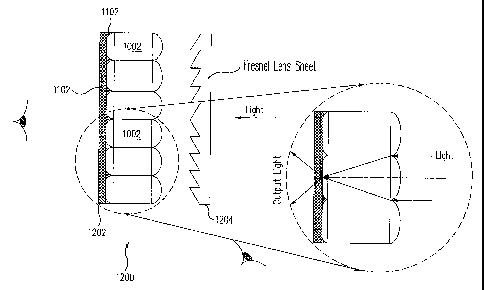
Display screen 1200 may also include a coating 1202 (e.g., a thin film coating
as
disclosed herein). A sheet 1204, such as for example a Fresnel~lens sheet, may
also be
included. As shown in FIG. 12, light is provided, which passes through display
screen 1200
to be viewed on the other side. By utilizing techniques disclosed herein, the
resulting output
light (i.e., the resulting light after passing through display screen 1200)
may have superior
qualities or performance as compared to conventional display screens.
As described herein, various embodiments of microlens arrays are disclosed.
For
example, in accordance with an embodiment of the present invention, a
microlens array is
disclosed which may be utilized to provide a high-quality display screen. The
display
screen may be inexpensive to manufacture relative to some conventional display
screens.
Furthermore, the display screen may offer improved performance relative to
some
conventional display screens, such as for example in terms of brightness and
uniformity,
contrast, and/or viewing angle
Embodiments described above illustrate but do not limit the invention. It
should also
be understood that numerous modifications and variations are possible in
accordance with
the principles of the present invention. Accordingly, the scope of the
invention is defined
only by the following claims.
14