Note: Descriptions are shown in the official language in which they were submitted.
CA 02554867 2006-07-31
WO 2005/074792 PCT/US2005/004834
3 NON-INVASIVE SPECTROSCOPY OF MAMMALIAN TISSUES
4
6 FIELD OF THE INVENTION
7 This invention relates to the non-invasive, spectrometric,
8 assessment of hemoglobin in the blood of mammalian tissues.
9
BACI<GROUND
11 The assessment of blood in mammalian tissues is important in
12 different scientific disciplines. In medicine, the assessment of blood,
13 and in particular, the assessment of hemoglobin concentration in the
14 blood, is important in the diagnosis and treatment of many diseases
and dysfunctions. In forensic science, the assessment of blood is an
16 indication of contusions or bruises of the skin, which are typical
17 consequences of blunt impact trauma. The invention concerns the
18 non-invasive, spectrometric, assessment of hemoglobin concentration
19 in blood in mammals. Two significant applications of this technology
are in the diagnosis of anemia, in which hemoglobin concentration is
21 assessed, and in the determination of blunt force trauma, in which
22 hemoglobin degradation and aging is assessed. These two
23 applications are discussed below.
24 A. Anemia
Anemia is often perceived by the general population to be a
26 minor medical condition. However, according to the World Health
27 Organization (WHO), anemia is the single, largest global illness
CA 02554867 2006-07-31
WO 2005/074792 PCT/US2005/004834
1 adversely affecting mortality and worker capacity. The United States
2 Department of Health & Human Services deems it a significant public
3 health concern. Of the 16 million people estimated to have anemia in
4 the United States, 78% go undiagnosed. In developing countries where
nutritional inadequacies and infectious diseases are more prevalent,
6 the situation is estimated to be even worse.
7 Anemia is a deficiency in the number of healthy red blood cells
8 in an individual's body. This deficiency results in oxygen deficiency in
9 the body's tissues and organ systems. Medically, anemia is defined by
the WHO as a hemoglobin concentration below 12 g/dL for females
11 and below 13 g/dL for males. Anemia is well known to the general
12 public to influence physical function by causing fatigue and weakness.
13 It also decreases myocardial function and increases peripheral arterial
14 vasodilation and activation of the sympathetic and reninangiotensin-
aldosterone system, which strongly influences the initiation or
16 progression of diseases such as heart failure and renal failure. In
17 addition, anemia affects individuals with other diseases; at least 33%
18 of cancer patients, 65-95% of HIV/AIDS patients, and 70% of
19 rheumatoid arthritis patients also have anemia.
Age-related disability and loss in physical function are mounting
21 public health concerns. Loss of physical function endangers the
22 quality of life and independence of many older adults and has
23 significant social and economic repercussions. The prevalence of
24 anemia increases with age and averages about 13% in persons' over 70
years of age. A majority of the anemia in aging adults signifies
2
CA 02554867 2006-07-31
WO 2005/074792 PCT/US2005/004834
1 diseases such as cancer and infectious ailments or are due to iron
2 deficiency or malnutrition. Recent studies indicate that anemia in
3 aging adults ins an independent risk factor for decline in physical
4 performance and is associated with higher mortality risl<s.
Yet anemia is severely under-diagnosed. The reasons are two-
6 fold. To determine if a patient is anemic, the physician can either
7 make a visual inspection of the palpebral conjunctiva of the eye socket
8 or take a blood sample and have a cell blood count (CBC) test run.
9 Visual inspection, dependent on the physician's experience and
training, is at best only 70J accurate and it has been shown that
11 physicians today are less accurate in diagnosing anemia by visual
12 inspection that in the past. Hung, et al., Evaluation of the Physician's
13 Ability to Recognize the Presence or Absence of Anemia, Fever, and
14 Jaundice, Academic Emergency Medicine 7.' 746-56 (2000). The CBC
test is very accurate, but painful and expensive to perform, time-
16 consuming and often not included in a routine examination.
17 Because of the need to assess hemoglobin concentration in a
18 more accurate and effective manner, a number of devices and methods
19 have been proposed. Exemplary are (i) retinal imaging, see United
States Patent No. 6, 305,804 entitled Non-Invasive Measurement of
21 Blood Component Using Retinal Imaging, (ii) blood oxygenation
22 monitoring, see United States Patent No. 6,456,862 entitled Method
23 for Non-Invasive Spectrophotometric Blood Oxygenation Monitoring
24 and United States Patent No. 6,149,589 entitled On-Line and Real-
Time Spectoreflectometry Measurement of Oxygenation in Patients
3
CA 02554867 2006-07-31
WO 2005/074792 PCT/US2005/004834
1 Eye, (iii) in-vivo imaging of blood, see United States Patent No.
2 6,104,939 entitled Method and Apparatus for Reflected Imaging
3 Analysis, (iv) blood analyzer technology, see United States patent
4 5,791,345 entitled Non-Invasive Blood Analyzer, and (v) image
processing of blood vessels, see United States Patent No. 4,99B,533
6 entitled Apparatus and Method for In Vivo Analysis of Red and White
7 Blood Cell Indices. None of these proposed solutions has been
8 embraced by health care professionals, predominately because of
9 inconvenience and inaccuracies in the results.
United States Patent Application Publication No. 2003/0002772,
11 published January 2, 2003 and entitled Non-Invasive Determination of
12 Blood Components discloses a method for estimating an amount of
13 hemoglobin in bodily fluids from the color of a tissue surface of a
14 subject by taking a digital color image of the surface of the subject
and a color reference object, decomposing the images into sub-
16 images of component colors having values corresponding to the pixels
17 of the images, selecting a window of each of the images, and
18 calculating an estimated level of hemoglobin using values associated
19 with the component values corresponding to the windows. Although
this approach is rapid, due to the inherent noise in this approach, the
21 accuracy of this method is limited.
22 Accordingly, there is still a significant need in the art for a
23 device that can quickly, accurately and non-invasively measure or
24 assess hemoglobin concentration. Such a device would have many
health care applications, such as in routine physical examinations, in
4
CA 02554867 2006-07-31
WO 2005/074792 PCT/US2005/004834
1 emergency rooms, for emergency rescue professionals, during surgery
2 for in-situ measurement of bleeding, for home health care for the
3 chronically ill and aging population, in developing countries lacking
4 medical facilities, in military medical units and in mass casualty
situations and triage units, and by oncology, pediatric, obstetric and
6 gynecology, anesthesiology, infectious disease, gastroenterology,
7 cardiology, nephrology, geriatric and urology specialists who deal with
8 anemia on a~regular basis.
9 B. Forensics
Visible contusions or bruises of the skin, the typical
11 consequence of blunt impact trauma, develop after the rupture of
12 blood vessels due to compressive or shearing forces imposed on the
13 body. Bruises are characterized as either subcutaneous or
14 intracutaneous, depending on the tissue layer that is affected. See
Bohnert, et al., Spectrophotometric Evaluation of the Colour of Intra-
16 and Subcutaneous Bruises, lnt'I,JoUrnal ofLegal Medicine 173(6): 343-
17 8 (2000). A subcutaneous bruise appears at the site of impact or
18 indirectly by local expansion or shifting of a hemorrhage. After a time
19 interval of hours to days, hemorrhages that are originally localized
deep in the tissue layers can extend toward the surface of the skin.
21 The bruise can change color over the course of time from blue to
22 green to yellow during the passing days as a result of the breakdown
23 and diffusion of hemoglobin. When the skin is forced by the
24 application of pressure into channel or profile, the blood is forced into
those sections of skin not exposed to the pressure, with hemorrhages
5
CA 02554867 2006-07-31
WO 2005/074792 PCT/US2005/004834
1 occurring as a result of vascular ruptures in the dermis. There have
2 been many studies on how to date bruising and how to distinguish
3 abusive bruising from accidental bruising. See for example, Bariciak,
4 et al., Dating Bruises in Children: an Assessment of Physician
Accuracy, Pediatrics 112(4), 804-7 (x003); Dunstan, et al., A Scoring
6 System for Bruise Patterns: A Tool for Identifying Abuse", Archives of
7 Disease in Childhood 86(5): 330-33 (2002) and Carpenter, The
8 Prevalence and distribution of Bruising in Babies, Archives ofDisease
9 in Childhood 80: 363-66 (1999). The color impression of a bruise, its
spectral signature and the extent of hemoglobin degradation are all
11 indicators of bruise age. Although a few recent studies of
12 spectrometric assessment of skin have been undertaken to diagnose
13 various skin diseases, we are aware of no studies relating to
14 spectrometric assessment of skin to assess bruise condition and age.
Assessments are routinely made by physicians without evidence-
16 based, scientific, support and there is currently no objective standard
17 or device for assessing bruises in mammals, especially humans.
18 Accordingly, there is also a compelling need in the art for a non-
19 invasive device and method to accurately age and assess the condition
of bruised tissue.
21
22 INVENTION SUMMARY
23 In one aspect, the invention provides a non-invasive
24 spectrometric device and method for assessing or detecting
hemoglobin concentration in mammalian tissues. More specifically,
6
CA 02554867 2006-07-31
WO 2005/074792 PCT/US2005/004834
1 the invention provides a non-invasive spectrometric device and
2 method for assessing or detecting hemoglobin concentration in
3 dermal and epidermal tissues of the skin in mammals. The device can
4 be used to detect hemoglobin concentration in an area of the skin that
has been subjected to bruising, in the palpebral conjunctiva area of
6 the eye socket, in the earlobe or in any other tissue surface.
7 Spectrometers are well know in the art. In operation, light
8 energy from a light source enters the spectrometer via an entrance slit,
9 passes through an objective lens, a diffraction grating and an exit slit.
The diffraction grating diffracts the light into its component
11 wavelengths and the wavelengths then strikes a detector that
12 generates a voltage in proportion to the intensity of the light hitting it.
13 The voltage drives a read-out device designed to provide the data on
14 the light's intensity. In early spectrometers, only one wavelength
could be detected and its intensity measured at a time. More recently,
16 the exit slit and detector have been replaced by an array of charge
17 coupled devices (CCDs), which has enabled measurement of more than
18 one wavelength at a time. (The number of wavelengths that can be
19 simultaneously measured is determined by the number of elements in
the CCD array.) The array generates an output that is used to
21 reconstruct the intensity of the light striking each element of the array.
22 This output is sent to a output device such as a monitor, a laptop
23 computer, a PDA (portable digital assistant) device, a printer or the
24 like.
7
CA 02554867 2006-07-31
WO 2005/074792 PCT/US2005/004834
1 In the spectrometric device of this invention the objective lens
2 and diffraction grating are replaced with a spectral imaging apparatus
3 based on electrically switchable color filter technology. The
4 spectrometric device of the invention comprises wavelength filter
means as the spectral imaging apparatus for transmitting or reflecting
6 wavelengths of light, light intensity sensor means arranged and
7 disposed to measure the intensity of the wavelengths transmitted or
8 reflected by the wavelength filter means and generate an electrical
9 signal from the wavelengths transmitted or reflected, output
processing means connected to the light intensity sensor means to
11 receive and process the output from the light intensity sensor means,
12 and display means connected to the output processing means to
13 display the output.
14 In one aspect, the light intensity sensor means is arranged and
disposed in stacked relation to the wavelength filter means such that
16 wavelengths of light are transmitted through the wavelength filter
17 means into the light intensity sensor means. In another aspect, the
18 light intensity sensor means is arranged and disposed in angular
19 relation to the wavelength filter means such that wavelengths of light
are reflected from the wavelength filter means into the light intensity
21 sensor means. In both of these aspects the light intensity sensor
22 means may be provided by an array of charged coupled devices (CCD)
23 or by a photodiode. The currently preferred embodiment employs a
24 CCD array.
8
CA 02554867 2006-07-31
WO 2005/074792 PCT/US2005/004834
1 The wavelength filter means comprises at least one pair of
2 planer substrates in parallel-opposed relation, at least one layer of
3 light-wavelength modulating material disposed between the pair of
4 planer substrates to achieve spectral coverage in the visible light
spectrum, and a power source in power-providing communication with
6 the substrate. The substrates will typically be composed of ITO-
7 coated glass or plastic such that electricity may be employed as the
8 source of power, but in one aspect of the invention described in detail
9 below, electrically conducting substrates are unnecessary because the
source of power is thermal. Three different types of Known light-
11 wavelength modulating materials may be employed in the wavelength
12 filter means: deformed helix ferroelectric liquid crystals, holographic
13 polymer dispersed liquid crystals, and cholesteric liquid crystals.
14 The light-wavelength modulating material, in one aspect,
comprises deformed helix ferroelectric liquid crystals (DH-FLC),
16 electrically tuned to exhibit pre-determined wavelength selection
17 properties. By "electrically tuned" we mean that when a voltage is
18 applied across the DH-FLC, the pitch of molecules elongates, which
19 correspondingly lengthens the wavelength of light exhibited. As in
understood in the art, the voltage applied to DH-FLC crystals varies
21 the pitch, which lengthens the wavelength of light transmitted or
22 reflected. Due to this fact, varying voltages can be applied to the DH-
23 FLC materials to set the materials to transmit or reflect at pre-
24 determined wavelengths. Typically DH-FLC have been employed in
display applications. In such applications, parallel boundary
9
CA 02554867 2006-07-31
WO 2005/074792 PCT/US2005/004834
1 conditions are employed. In the DH-FLC of this inventions, the
2 molecules in the layers of the DH-FLC employed are aligned
3 perpendicular to the surfaces of the planer substrates, i.e.
4 homeotropic alignment. This modification achieves the reflective
capacity of the material.
The power source employed to modulate the DH-FLC can be
7 either electrical power or thermal power. For thermal power
8 applications, a transparent resistive heater or other thermal power
9 source is positioned on the planer, exterior, surface of one of the
substrates, which are not ITO coated. For electrical power
11 applications, the electrical power source is connected to the
12 conducting elements, the ITO coating, of the substrate to create an in-
13 plane electric field using well-Know techniques in the art.
14 In another aspect, the spectrometric device of the invention
includes light-wavelength modulating material composed of
16 holographic polymer dispersed liquid crystals (H-PDLC) disposed
17 between electrically conducting substrates. In this aspect, the light
18 wavelength modulating material and electrically conducting substrates
19 are arranged in a stack. The stack is composed of a plurality of layers
of H-PDLC arranged in alternating, superposed, relation to a plurality
21 of substrate layers. The number of substrate layers equals the number
22 of layers of H-PDLC, plus one. In other words, the wavelength
23 modulating material includes alternating layers of, from bottom to top,
24 substrate and H-PDLC in a stack with the top layer being a layer of the
substrate. Each side of the substrate layer adjacent to H-PDLC will
CA 02554867 2006-07-31
WO 2005/074792 PCT/US2005/004834
1 have an electrical conducting coating, for example indium-tin-oxide
2 (1T0) in order to complete the circuit. Consequently, the top and
3 bottom layers of substrate may have an electrical conducting coating
4 on only the side, the side disposed interiorly and adjacent to the H-
PDLC. The stack may be composed of as many alternating layers of
6 electrically conducting substrate and H-PDLC as is desired but
7 preferably the stack will be composed of between two and ten layers of
8 H-PDLC (and therefore between three and eleven layers of substrate).
9 In one embodiment of this aspect of the invention, the stack is
composed of one layer of H-PDLC sandwiched between two layers of
11 electrically conducting substrate. In this aspect, there exists in the H-
12 PDLC film a variable index of refraction of the liquid crystal, which is
13 different from the index of refraction of the polymer. This variable
14 index of refraction permits continuous modification of the reflection or
transmission peak, thereby eliminating the need for multiple
16 "gratings", each providing reflection or transmission at a single peak.
17 These variable refraction index H-PDLC and their operation are
18 described in detail in United States Patent Publication No.
19 ZOOZ/0130988 herein incorporated by reference.
In an alternate embodiment of the invention, the light-
21 wavelength modulating material is composed of cholesteric liquid
22 crystals (CLC) disposed between electrically conducting substrates. In
23 this embodiment the CLC may also be composed a plurality of CLC
24 layers arranged in alternating, superposed, relation to a plurality of
substrate layer. In this case, the stack will have a number of substrate
11
CA 02554867 2006-07-31
WO 2005/074792 PCT/US2005/004834
1 layers one greater than the number of CLC layers and the power
2 source will produce electrical energy perpendicular to the pitch axis of
3 the CLC layers.
4 The CLC layers have the capacity to reflect light of different,
per-determined wavelengths, but because they are inherently reflect
6 light in a right or left handed manner, the maximum efficiency will be
7 only 50%. Consequently, to increase the efficiency, the device may
8 further include a passive optical element such as a quarter-wave plate
9 disposed in parallel relation between two reflective CLC of opposite-
handedness.
11 In another aspect, one CLC layer may be interposed between two
12 electrically conducting substrate layers. In this aspect, there exists in
13 the CLC film a variable index of refraction of the liquid crystal, which is
14 different from the index of refraction of the polymer. Like the variable
refraction index H-PDLC, the variable index of refraction in the CLC
16 permits continuous modification of the reflection or transmission
17 peak, thereby eliminating the need for multiple "gratings", each
18 providing reflection or transmission at a single peak.
19 The output processing means connected to the light intensity
sensor means to receive and process the output from the light
21 intensity sensor means can be any of the well-Known output
22 processing means employed in spectrometers. Likewise, the display
23 means connected to the output processing means to display the
24 output can be configured using well-known techniques in the art to
display indicia of the estimated level of hemoglobin detected.
12
CA 02554867 2006-07-31
WO 2005/074792 PCT/US2005/004834
1 In the operation of the device of the invention, light is projected
2 from the area of epidermal tissue of interest into the device and is
3 then filtered by the wavelength filter means and detected by the light
4 sensor means of the device, the latter of which generates an electrical
signal from the wavelengths transmitted or reflected and transmits
6 that signal to the output processing means, which processes the
7 output and transmits it to a display readable by a physician or other
8 health care professional. The basics of how spectrometers and other
9 spectroscopic tools (such as, for example, spectrophotometers) work
is well Known in the art and succinctly described in Steven L. Brown,
11 "Laboratory Techniques for General Chemistry, Ch. 5, Spectroscopy" ,
12 2002, Hayden-McNeil Publishing, Plymouth, Michigan.
13 The invention also includes a method of detecting or assessing
14 the concentration of hemoglobin in a mammalian subject suspected of
having an abnormal hemoglobin concentration. The method comprises
16 the steps of (a) exposing an area of tissue of a mammalian subject
17 suspected of having an abnormal hemoglobin concentration to a
18 spectrometer of the invention to receive and analyze light reflected
19 from the area of tissue; (b) reading the output from the spectrometer
2o indicating the hemoglobin concentration in the area of tissue exposed
21 to the spectrometer; and (c) comparing the hemoglobin concentration
22 of the output to the hemoglobin concentration in a control standard
23 for a normal epidermal tissue specimen.
24
DESCRIPTION OF THE DRAWINGS
13
CA 02554867 2006-07-31
WO 2005/074792 PCT/US2005/004834
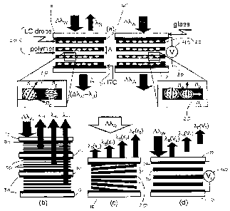
1 Fig. 1 is an illustration of a H-DPLC containing device. In (a) the
2 prior art panel is illustrated in its voltage-off and voltage applied
3 positions. In (b) and (c) two embodiments of the device of the
4 invention are illustrated in which only one layer of H-DPLC is
employed.
6 Fig. 2 is a graphic representation of the transmission results (a)
7 and the reflection results (b) for the stack of five H-DPLC layers
8 described in detail below.
9 Fig. 3 illustrates the mode of operation of a prior art CLC panel
(a) in planar (left), focal conic (middle) and homeotropic (right) states.
11 In (b) an embodiment of the invention composed of a stacl< of three
12 CLC panels is illustrated. In (c) an embodiment of the invention
13 composed of one CLC in IPS mode is illustrated.
14 Fig. 4 is a graphic representation of the transmission results (a)
and the reflection results (b) for a CLC device composed of three panel
16 pairs to reflect read, green and blue as described in detail below.
17 Results are shown in (c) for a single panel CLC IPS device that nearly
18 covers the entire spectral range as described in detail below.
19 Fig. S illustrates the device of the invention comprising DH-FLC
crystals subject to in-plane switching to produce a red-shift.
21 Fig. 6 is a graphic representation of the transmission results (a)
22 and reflection results (b) as temperature varies in the DH-FLC
23 containing device of the invention.
24
DETAILED DESCRIPTION
14
CA 02554867 2006-07-31
WO 2005/074792 PCT/US2005/004834
1 In the spectrometric device of this invention the objective lens
2 and diffraction grating are replaced with a spectral imaging apparatus
3 based on electrically switchable color filter technology. The
4 spectrometric device of the invention comprises wavelength filter
means as the spectral imaging apparatus for transmitting or reflecting
6 wavelengths of light, light intensity sensor means arranged and
7 disposed to measure the intensity of the wavelengths transmitted or
8 reflected by the wavelength filter means and generate an electrical
9 signal from the wavelengths transmitted or reflected, output
l0 processing means connected to the light intensity sensor means to
11 receive and process the output from the light intensity sensor means,
12 and display means connected to the output processing means to
13 display the output. The light intensity sensor means may take the
14 form of an array of charge coupled devices (CCDs) or a photodiode.
The output processing means and display means are both well-
16 recognized elements of spectrometric devices and need not be
17 described in detail here as the skilled artisan would be able without
18 undue experimentation to arrange, connect and incorporated these
19 elements. Any of the well-known output processing means and
display means known in the art may be used.
21 In one aspect, the light intensity sensor means is arranged and
22 disposed in stacked relation to the wavelength filter means such that
23 wavelengths of light are transmitted through the wavelength filter
24 means into the light intensity sensor means. In another aspect, the
light intensity sensor means is arranged and disposed in angular
CA 02554867 2006-07-31
WO 2005/074792 PCT/US2005/004834
1 relation to the wavelength filter means such that wavelengths of light
2 are reflected from the wavelength filter means into the light intensity
3 sensor means.
4 The wavelength filter means comprises at least one pair of
planer substrates in parallel-opposed relation, at least one layer of
6 light-wavelength modulating material disposed between the pair of
7 planer substrates to achieve spectral coverage in the visible light
8 spectrum, and a power source in power-providing communication with
9 the substrate. The substrates will typically be composed of ITO-
coated glass or plastic such that electricity may be employed as the
11 source of power, but in one aspect of the invention described in detail
12 below, electrically conducting substrates are unnecessary because the
13 source of power is thermal. Three different types of Known light-
14 wavelength modulating materials may be employed in the wavelength
filter means: holographic polymer dispersed liquid crystals (H-PDLC),
16 cholesteric liquid crystals (CLC), and deformed helix ferroelectric liquid
17 crystals (DH-FLC). These types of liquid crystals are well-I<nown in the
18 art. Their use, including the modifications necessary or desirable to
19 employ them in the spectrometric device of the invention, is described
in detail below.
21 A. H-PDLC containing devices
22 Holographic polymer dispersed liquid crystals are created by a
23 simple one-step fabrication process in which a homogeneous mixture
24 of photosensitive propolymer and nematic liquid crystal is exposed to
an interference pattern process following the method disclosed in
16
CA 02554867 2006-07-31
WO 2005/074792 PCT/US2005/004834
1 Bowley and Crawford, "Diffusion I<inetics of Formation of Holographic
2 Polymer Dispersed Liquid Crystal Display Materials", 2000, Applied
3 Physics Letters 76. In the bright regions of the interference pattern
4 the polymerization occurs more rapidly that in the ~darl< regions,
forcing the non-reactive liquid crystal out of the bright regions and
6 into the dark regions. This diffusion process creates a stratified
7 material composed of liquid crystal droplets and polymer rich layers
8 that is locked-in by the photo-polymerization process. The grating
9 pitch is given by n= ~f//2<n>sin 8, where ~f/is the wavelength of the
exposing laser beams, <n> is the average index of refraction of the
11 liquid crystal and polymer mixture , and 2 0 is the angle between the
12 exposure beams inside the sample. Since the liquid crystal typically
13 has an average index of refraction that is larger than that of the
14 polymer, a spatial perturbation in the index of refraction exists.
The principle is illustrated in Fig. 1 (a). The H-PDLC includes
16 liquid crystal and matrix polymer layers (20) which form a reflection
17 grating capable of reflecting a wavelength of light disposed between a
18 pair or more than one pair of electrically conducting substrates (10),
19 which may be formed from indium-tin-oxide (ITO)-coated glass or
plastic. See for example, PCT Patent Publication WO O1 /20406
21 published 22 March 2001, which discloses a multicolored reflection
22 liquid crystal display device in which the liquid crystal film is capable
23 of reflecting two different wavelengths of light. Each electrically
24 conducting substrate layer (10) is connected with a means for
17
CA 02554867 2006-07-31
WO 2005/074792 PCT/US2005/004834
1 providing electrical energy through the electrodes of the conductant
2 (30) and into the H-PDLC (20).
3 In the absence of an applied voltage, a refractive index
4 modulation exists between the liquid crystal rich planes (shown as
droplets) and the pure polymer planes of the H-PDLCs. The average
6 index of refraction of the liquid crystal rich layers, n~c, is some
7 combination of the ordinary, n0, and the extraordinary, ne, index of
8 refraction of the liquid crystal, which is estimated as n~c Z ~ (ne2 +
9 Zno~)/3. When the material is illuminated with a broadband white-
light source, a narrow reflection band is rejected with reflectives
11 greater than 50% and peal< widths in the 15-30 nm range depending
12 on the birefringence of the liquid crystal, index of refraction of the
13 polymer, and sample thicleness. Since liquid crystal molecules possess
14 a positive dielectric anisotropy they align parallel to the applied
electric field when an external voltage (40) is applied. In the aligned
16 state, the ordinary refractive index of the liquid crystal matches that of
17 the polymer and the index modulation vanishes. The H-PDLC (20)
18 becomes transparent to all wavelengths, as shown in Fig. 1 (a), right
19 panel. Switching voltages in the range of 50-100 volts are needed,
since the liquid crystal is highly constricted by the holographic planes
21 of dimensions 170-200 nm for visible reflections; however, the
22 response times can be very fast, in some cases, less than 100 p
23 seconds.
24 In one embodiment of the current invention, these HPDLCs are
employed as a spectrometric device. This embodiment is illustrated in
18
CA 02554867 2006-07-31
WO 2005/074792 PCT/US2005/004834
1 Fig 3(b), in which the spectrometric device comprises a plurality of
2 planer H-PDLC film layers disposed in alternating, stacking relation
3 with a plurality of planer ITO-coated substrate layers. The H-PDLC
4 stratified films are sandwiched between the ITO coated glass
substrates and maintained at a distance of between about 2 to about
6 30 micronmeters. Between 2 and ZO H-PDLC film layers, and therefore
7 between 3 and 21 substrate layers may be employed. Preferably,
8 between 2 and 10 layers of H-PDLC and therefore between 3 and 1 1
9 substrate layers may be employed. Electrical leads 30 are then
connected to the edges of each of the planer ITO glass substrates so
11 the H-PDLC material can be exposed to an applied voltage. When a
12 voltage is applied, an electric field is created within the material and
13 the H-PDLCs can be tuned to a transparent state. By using multiple H-
14 PDLC layers, various wavelengths can be allowed to pass through the
stack by applying different voltages to the different substrate layers.
16 In Fig. 1 (b), the stack is shown with broad band incident white light,
17 ~~W, and three reflection bands 7~8~, 7~B2,~g3,whose peak wavelength is
18 dictated by Bragg's law, 7~B = 2d<n> for normally incident light, where
19 dis the thickness of the holographid plane. In the embodiment
illustrated in Fig. 3(b), a stack of three H-PDLC layers is shown but the
21 device may be constructed with more or less than three layers to
22 generate a number of reflection bands corresponding to the number of
23 H-PDLC layers in the stack.
24 In another embodiment, the stack is composed of five H-PDLC
film layers interspersed between planer ITO-coated substrates instead
19
CA 02554867 2006-07-31
WO 2005/074792 PCT/US2005/004834
1 of three layers as described above. Fig. 2 is a graphic representation
2 of data for such a stack in transmission, Fig. 2(a) and in reflection, Fig.
3 2(b). In reflection (Fig. 2(b)), the five-layered H-PDLC stack exhibits
4 between 30-40% reflectance in the wavelength range between about
600 and 760 ~ [nm].
6 Referring again to Fig. 1, parts (c) and (d) illustrate two alternate
7 embodiments of this aspect of the inventions. In the aspect illustrated
8 in (c), only one H-PDLC film is needed and employed because a spatial
9 gradient has been created in the holographic plane sizes from one
edge of the sample to the other. The H-PDLC sample can then act as a
11 wavelength modulating material for multiple wavelengths. In order to
12 selected different wavelengths, the ITO coating can be pixilated so that
13 the various wavelengths can be electrically addressed independently.
14 In the alternate embodiment shown in (d), only one H-PDLC film
is needed and employed because there exists in the H-PDLC film a
16 variable index of refraction of the liquid crystal, which is different from
17 the polymer. In this way, as the electric field is applied to the two
18 substrates, and the index of refraction changes with respect to the
19 index of the polymer enabling the H-PDLC to be electrically addressed
to a pre-determined wavelength. This alternate embodiment is
21 described in detail in PCT Patent Publication WO O1 /20406 published
22 22 March 2001, which is herein incorporated by reference.
23 All of these above embodiments of H-PDLC can be used in the
24 non-invasive, spectrometric device of the invention to assess
hemoglobin concentration in the blood of mammalian tissues.
CA 02554867 2006-07-31
WO 2005/074792 PCT/US2005/004834
1
2 B. CLC containing devices
3 Cholesteric liquid crystals (CLC) are also Known in the art. CLC
4 exhibit long-range, orientational order analogous to conventional
nematic liquid crystals, except that the molecules are chiral. See
6 Blinoff and Chigrinov, Electro-Optic Effects in Liquid Crystals, Springer,
7 New York, (1994). Consequently, the structure acquires a
8 spontaneous right-handed or left-handed twist about a helical axis
9 normal to the average direction of the liquid crystal molecules. The
degree of twist of the phase is characterized by the cholesteric pitch,
11 "P". Heretofore, CLC have been used in flat -panel display
12 applications. See Yang, et al., in Liquid Crystals in Complex
13 Geometries Formed by Polymer and Porous Networks, Crawford, GP
14 and Sumer, S, eds., Taylor & Francis, London (1996); Doane, et al.,
Cholesteric Liquid Crystals for Flexible Display Applications, John Wiley
16 & Sons, London, (2004). The operation of a CLC device is illustrated in
17 Figure 3(a)left panel. In the zero voltage state illustrated in the left
18 panel, the molecules are aligned in the planar configuration between
19 the substrate layers, and since the structure is periodic, they can
reflect a bandwidth centered at Via, which is dictated by Bragg's law (~B
21 = <n>P for normal incidence). Upon application of an applied voltage
22 (V~ ~ 10-15 volts for a 5 pm sample), a positive dielectric anisotropy
23 material (~~>0) transforms to a focal conic state, which is
24 characterized by a random distribution of helical pitches, as shown in
Fig. 3(a), middle panel. This state is transparent and remains that way
21
CA 02554867 2006-07-31
WO 2005/074792 PCT/US2005/004834
1 even after the voltage is removed. In other words, this device
2 possesses bi-stable memory since the focal conic state can remain
3 indefinitely even after the field is removed. Upon application of a
4 higher voltage (Vz ~ 25-30 volts), the material transforms to the
hometropic, aligned, state as shown in Fig. 3(a), right panel. When the
6 voltage is abruptly removed, the homeotropic state transforms back to
7 the reflective planar state. Fig. 3(a) right panel. The chiral pitch can be
8 engineered, or set, by mixing in different concentrations the chiral
9 components to reflect in the ultraviolet, visible and near infrared in
accordance with art-recognized tehchniques. The switching time is on
11 the order of 30-50 ms dower, depending on the mode, than other
12 liquid crystal materials.
13 In order for CLC to be used in a non-invasive spectrometer, full
14 spectral coverage in the visible light spectrum is required. This can be
achieved by employing a CLC stack, comprising a plurality of layers of
16 cholesteric liquid crystal materials. Fig. 3(b) illustrates a three-stack
17 of CLC panels that reflect red, green and blue. Fig. 4(a) presents the
18 data for this stack in the transmission mode and Fig. 4(b) presents the
19 data for this stack in the reflection mode upon application of the
applied voltage. Since CLC are intrinsically right- or left-handed
21 because of their chirality, they can reflect only right-handed or left-
22 handed, circularly polarized, light, ideally with 50J efficiency at the
23 Bragg wavelength. To solve this problem, we disposed and arranged
24 the panels that reflected red, green and blue as panel pairs, each color
having a right handed and a left handed panel forming the respective
22
CA 02554867 2006-07-31
WO 2005/074792 PCT/US2005/004834
1 pairs, so that we actually had six panels in the stack, two red, then two
2 green, then two blue. We then integrated a passive optical element
3 between two identically reflecting panels to achieve a much higher
4 efficiency, exceeding BO%, as shown in Fig. 4(a) and (b). In the
embodiment illustrated the passive optical element employed was a
6 quarter-wave plate, but the skilled artisan will recognize that any
7 passive optical element could be used. Alternatively, to achieve the
8 same outcome, a left handed panel and a right handed panel with the
9 same 7~B can be stacked.
l0 The stacked solution illustrated in Fig. 4(b) was experimentally
11 evaluated and the results are shown in Fig. 5(a) and (b). The full
12 spectral width of the reflection peak in Fig. 4(b) is O~FWHM>100nm.
13 The spectral width is largely dictated by the birefringence of the CLC
14 material, Vin. To decrease the spectral bandwidth, materials with a
lower ~n can be employed. For example, for a material with a
16 On~0.05, bandwidths on the order of D~FwHM~30nm for 7~B = 600nm
17 can be achieved. Because CLC materials do not have the scattering
18 losses observed with H-PDLC materials, numerous panels can be
19 stacked to achieve full spectral coverage in the visible range.
A CLC in-plane switching (IPS) mode is shown in Fig. 4(c) in
21 which field direction is parallel to the substrates, orthogonal to how it
22 was applied in Fig. 4(a) and (b). As an in-plane voltage is applied
23 perpendicular to the pitch axis of the CLC, the pitch elongates and the
24 reflection red-shifts. This IPS mode permits the use of one panel to
span nearly the entire visible spectral range, as is shown in Fig. 4(c).
23
CA 02554867 2006-07-31
WO 2005/074792 PCT/US2005/004834
1 This mode enable electrical tuning of the reflection band from 450 nm
2 to 700nm. Assuming linearity in the transition region, the
3 tunability/resolution metric is OV/07~~ 0.1 5 V/nm for the peak
4 maximum. The downside of this approach is that overall efficiency
may be reduced because the electrodes on the surface of the substrate
6 reduce the optical throughput, as CLC materials do not respond above
7 the electrode. By offsetting a pair of transparent conducting
8 electrodes on the top and bottom substrates and by driving them with
9 voltage signals out of phase, this problem is alleviated. In addition,
because the switching voltage is higher in the CLC IPS mode as
11 compared to conventional IPS mode, the electrodes must be arranged
12 closer together so that maximum drive voltages do not exceed 40-50
13 volts. The preferred distance between electrodes is around 5 ~tm, but
14 the skilled artisan will recognize that distance between electrodes can
be optimized for various materials without any undue
16 experimentation.
17 C. DH-FLC
18 The art-known ferroelectric liquid crystal, or chiral smectic C
19 phase (SmC) liquid crystals, consists of layers of molecules. This
thickness of the chiral smectic C layers are less than one molecular
21 length. See Yeh and Gu, Optics of Liquid Crystals, john Wiley, New
22 York, (1999). As a result, the molecules must tilt at an angle with
23 respect to the layer normal. Because the tilt angle is fixed, the
24 molecular orientation is confined to a cone with a half apex angle of 0.
Ferroelectric liquid crystal materials have intrinsic chirality and
24
CA 02554867 2006-07-31
WO 2005/074792 PCT/US2005/004834
1 associated pitch, much like CLC materials, and they have a dipole
2 moment perpendicular to the long molecular axis, rather than parallel
3 to it as in the case of CLCs materials. In ferroelectric switching, the
4 molecules switch on the cone.
Art-Known, deformed helix ferroelectric liquid crystal materials
6 (DH-FLC) were first used in display applications. See Verhulst, et al., A
7 Wide Viewing Angle Video Display Based on Deformed Helix
8 Ferroelectric LC and Diode Active Matrix, Proceeding ofthe
9 /nternational Display Research Conference 94.' 377-80 (1994). In
those applications, parallel boundary conditions were employed, i.e.,
11 the molecules are aligned in parallel to the substrate surfaces In this
12 embodiment of the invention, homeotropic alignment, wherein the
13 molecules are aligned perpendicular to the substrate surfaces, should
14 be employed so that the panel provides a wavelength selection
property similar to the CLC panel. Dynamic switching times for panels
16 of DH-FLC materials operated as described above should be less than
17 500 ps.
18 This embodiment is illustrated in Fig. 5. Pitch is deformable
19 using temperature or an in-plane electric field. If an in-plane electric
2o field is employed, the helix deforms or elongates and the reflection
21 red-shifts. If the in-plane switching (IPS) mode described above for
22 CLC materials is employed, the same disadvantages described will
23 result and accordingly, the IPS electrodes should be located closer
24 together to minimize aperture loss. A preferred range is about 5 pm,
but the skilled artisan will recognize that distance between electrodes
CA 02554867 2006-07-31
WO 2005/074792 PCT/US2005/004834
1 can be optimized for various materials without any undue
2 experimentation. If temperature is employed to accomplish switching,
3 a transparent resistive heater may be incorporated into the device and
4 employed in place of electric power in accordance with well-
s recognized methods. A DH-FLC panel having homeotropic alignment
6 at the surfaces, i.e., in which the molecules are aligned perpendicular
7 to the plane of the layer was prepared and subjected to temperature
8 increases. The data is presented in Fig. 6(a) and (b) for transmission
9 and reflection, respectively. Since the refractive index of the material
was, small and the cone angle was around 30 degrees, the sample was
11 tilted with respect to the incident light to increase the index
12 perturbation with respect to the incoming light. One DH-FLC panel
13 can cover the entire visible spectral range, as is illustrated in Fig.
6(c).
14 Assuming linearity in the transition region if Fig. 6(c), the
tenability/resolution metric is OV/~~ ~ 0.12 °/nm.
16 The DH-FLC panels of the invention may be switched either
17 electrically or thermally. Electrical switching is currently the preferred
18 mode. Lil<e the CLC-containing devices of the invention , electrical
19 switching may be accomplished by advantageous employment of the
herein disclosed IPS mode, in which the field direction is parallel to the
21 substrates. Thermal switching can be accomplished by employing a
22 transparent resistive heater, which is connected to a power supply
23 (typically a current source) employing methods and materials well-
24 Know in the art.
26
CA 02554867 2006-07-31
WO 2005/074792 PCT/US2005/004834
1 Other embodiments are within the scope and spirit of the
2 claims. Certain elements and functions of the invention described
3 above can be implemented using software, hardware, firmware,
4 hardwiring, or any combinations of these in art-recognized ways.
Features, elements and means of the invention implementing various
6 functions may be physically located at various positions rather than in
7 a single location or apparatus.
8 All references cited in this document are hereby incorporated by
9 reference herein for the substance of their disclosure.
to
27