Note: Descriptions are shown in the official language in which they were submitted.
CA 02555960 2006-08-10
WO 2005/078918 PCT/SE2005/000197
Zoad-Invariant Amplifier
Technical Area
The present invention relates to electronic amplification.
More specifically, the invention relates to biasing of linear
push-pull power amplifiers.
Background Art
Electronic amplifiers have found their way into applications
such as e.g. audio reproduction. Audio may be represented by
a low-level electrical signal. In the process of transforming
such a signal into sounds perceivable by the human ear, it is
amplified in terms of voltage and/or current and forwarded to
an electromechanical transducer, i.e. a loudspeaker.
Electrical amplification is accomplished by using a so-called
power amplifier.
The vast majority of power amplifiers today fox linear
applications such as audio reproduction are push-pull
amplifiers. Such amplifiers employ disparate first and second
circuitry for sourcing and sinking current respectively to a
load such as a loudspeaker. Henceforth, the first circuitry
will be referred to as sourcing circuitry, and the second
circuitry will be referred to as sinking circuitry. Their
constituent parts will be denoted correspondingly.
The sourcing circuitry thus sources current and therefore is
connected to a positive voltage supply terminal of a power
supply, while the sinking circuitry sinks current and
therefore is connected to a negative voltage supply terminal
of the power supply. Each of the sourcing and sinking
circuitry has one or several power handling output devices
connected serially or in parallel.
1
CA 02555960 2006-08-10
WO 2005/078918 PCT/SE2005/000197
Active power output devices, i.e. valves or power transistors
are inherently non-linear, particularly when currents are
low. In push-pull amplifiers, this causes crossover
distortion. Crossover occurs when load current switches
direction, i.e. when handling of load current switches from
one or a set of sourcing output devices to one or a set of
sinking output devices or vice versa.
A means to lower the impact of non-linearity inherent in
active output devices, and subsequently to lower crossover
distortion, is to traverse a quiescent current through the
sourcing and sinking output devices. By properly drawing a
quiescent current through the output devices, they are forced
to operate in a more linear region when load current is low.
This is called biasing. Amplifiers that operate in this way
are traditionally said to operate in class A or class AB.
Traditional class A amplifiers are biased to provide through-
conduction of quiescent current at all times while the
amplifier is in operation, for all permissible loads. A
drawback is that the quiescent current often becomes very
large, with resulting large internal power dissipation. In
traditional class AB amplifiers, the quiescent current is
much lower but load currents above some generally quite low
level force the active output devices that do not carry the
load current at any given point in time to cut off, thereby
causing some crossover distortion.
In the art, it is known to prevent cut off while keeping the
quiescent current in the same order of magnitude as for a
traditional class AB amplifier, thus overcoming traditional
class A amplifier shortcomings without introducing
significant crossover distortion.
In some applications it is important that power amplifiers
have very low output impedance. For example, designers of
2
CA 02555960 2006-08-10
WO 2005/078918 PCT/SE2005/000197
high performance loudspeakers generally model power
amplifiers as perfect or near perfect voltage sources. Thus,
the output of a model power amplifier substantially maintains
a voltage proportional to the input signal, irrespective of
impedance variations caused by reactive components of the
loudspeaker. This means that parts that together constitute a
loudspeaker, i.e. cabinets, speaker elements, ports,
crossover filters and so fourth are designed to produce a
desired sound when a power amplifier connected to the
loudspeaker has low output impedance. Accordingly, power
amplifiers suitable for high performance loudspeakers
generally have low output impedance. Achieving low output
impedance is however by no means trivial, or has substantial
drawbacks.
Global negative feedback is often employed in power
amplifiers. Global negative feedback lowers the output
impedance. The impedance reduction that can be achieved
through global negative feedback is however dependent on the
amount of feedback that can be applied. A certain amount of
global negative feedback usually has its merits and is often
even quite necessary, but extensive negative feedback
compromises stability. If loop gain, being the product of
forward and feedback gain is too high with respect to
available bandwidths and other stability criteria, distortion
increases and self-oscillation may even be induced.
Paralleling of power handling output devices also brings down
output impedance. Depending on design and types of output
devices, paralleling may cause various well-known
implications such as difficulties in achieving appropriate
current sharing between the paralleled output devices.
In solid-state amplifiers, so-called degeneration resistors,
also known as emitter or source resistors, are often fitted
3
CA 02555960 2006-08-10
WO 2005/078918 PCT/SE2005/000197
in the amplifier's output stage, at the amplifier's power
handling transistors. This is particularly so in discrete
designs where current sensing can not easily be carried out
on the active output devices because of process variations,
thermal variations and difficulties in achieving thermal
proximity with other components. Current sensing is generally
required for efficiently controlling the quiescent current.
Reduced impedance degeneration resistors lower the output
impedance of the amplifier. Biasing however generally becomes
more difficult, since control of quiescent current becomes
more critical.
Low output impedance can also be accomplished by employing
local positive feedback, though stability and biasing may be
detrimentally affected.
Some applications require Direct-Current (DC) amplification.
Such a requirement rules out amplifier designs that
implicitly carry out high-pass filtering or designs that
otherwise degrade signals that have a DC offset voltage.
In some applications, including quality audio reproduction,
measures are sometimes taken to eliminate or reduce unwanted
DC voltages being present at the output of intrinsically DC
coupled amplifiers. Even so, internal DC amplification is
often advantageous since control of low-frequency response
can be simplified and made more precise e.g. through DC servo
arrangements that provide low frequency negative feedback.
Conversely, lack of ability to amplify DC signals may be
disadvantageous.
Examples from the prior art pertinent to output impedance
and/or biasing are shown below.
In US-patent number 5,389,894, Ryat discloses a power
amplifier comprising an input amplifier gain stage, a bias
4
CA 02555960 2006-08-10
WO 2005/078918 PCT/SE2005/000197
circuit for enabling class AB operation and a sourcing and a
sinking output transistor in a push-pull output stage. The
gain stage supplies a signal drive current only to the
sourcing output transistor, while the sinking output
transistor receives its drive current from the bias circuit.
Thus, the signal drive current from the gain stage to the
sourcing transistor is separate from the drive current from
the bias circuit to the sinking transistor. The object is to
provide high drive capability, high voltage swing, and an
amplifier that does not suffer from high output impedance
under high current conditions.
The power amplifier disclosed by Ryat employs design
principles that presuppose close thermal coupling and closely
matched component s Such an environment is generally found in
monolithic integrated circuits. Discrete designs on the other
hand generally have to cope with significant parameter
spreads due to differing reciprocal temperatures and process
variations.
For example, to sense currents through the output
transistors, Ryat uses second transistors that share Vbe-
voltages with the output transistors, for generating second
currents proportional to the currents through the output
transistors. Thus, current sensing is carried out on the
output transistors. As previously said, this is not easily
done in discrete designs, particularly with some types of
output devices such as MOSFETs where process and temperature
variations have gross impact on the electrical properties.
Moreover, the bias control and the output transistor drive
circuitry are asymmetric. Asymmetry is generally known to
cause problems, e.g. distortion, DC voltage operating point
offset or drift with changing temperature.
5
CA 02555960 2006-08-10
WO 2005/078918 PCT/SE2005/000197
In US-patent number 5,055,797, Chater discloses a push-pull
power amplifier having automatic bias control. Output
currents from sourcing and sinking output transistors of the
output stage of the amplifier are determined by sensing
voltages across sourcing and sinking sensing resistors, the
sensed voltages being proportional to the output currents.
The sensed voltages are added and the resulting sum signal is
operated upon for extracting a signal proportional to a peak
minimum value. The signal being proportional to the peak
minimum value is used in a negative feedback loop for
controlling the quiescent current of the amplifier. The
object is to provide a method of bias control that is not
dependent on thermal variations of the output transistors, is
unaffected by the presence or absence of an output signal,
and that accordingly reduces crossover distortion.
The biasing scheme of Chater has little effect on output
impedance. Furthermore, the amplifier is not DC coupled. If
it were, it would be insufficiently biased for DC signals
since the peak minimum value would not unconditionally
represent the quiescent current in the presence of a load
current.
In US-patent number 4,439,743, a biasing circuit is shown for
reducing distortion in power amplifiers caused by non-linear
amplifying elements. This is accomplished by excluding output
transistors in the signal transmission path of the biasing
circuit.
In US-patent number 4,489,283 there is disclosed a power
amplifier having a fixed and a variable biasing circuit. The
variable biasing circuit enables full cycle conduction of
power-amplifying elements. This is achieved by sensing
control voltages (Vbe) of the power amplifying elements and
in response thereto providing calibration currents used for
6
CA 02555960 2006-08-10
WO 2005/078918 PCT/SE2005/000197
controlling the power amplifying elements in suoh a way as to
prevent cut-off during a full signal cycle.
In US-patent number 5,977,829, an amplifier having a variable
quiescent current is shown. At low output power levels, a
biasing circuit provides a reduced biasing current to the
input stage of the amplifier, while at higher output power
levels the biasing current is augmented in order to reduce
distortion.
In US-patent number 6,188,269 there is disclosed a rail-to-
rail amplifier having a bias-current that is substantially
independent of process variations, temperature and supply
voltage. A sub circuit mimics an idle output stage. A bias
voltage is generated in response to a current through the sub
circuit. The bias voltage in turn controls the quiescent
current through an output stage.
In US-patent number 4,558,288 there is disclosed an emitter-
follower type push-pull output stage in which a bias circuit
prevents cut-off of output transistors, thereby decreasing
crossover distortion.
In US-patent number 4,885,674 there is disclosed a load-
independent switch-mode power converter. The invention
features a positive current-feedback loop that compensates
for varying voltage drops caused by load variations.
In the prior art there are thus known various biasing schemes
and methods to lower output impedance of an amplifier and to
prevent cut-off. However, there is yet room for substantial
improvement.
A problem in the art is to devise a push-pull amplifier that
has a simple mechanism for reducing output impedance without
introducing the disadvantages previously discussed.
7
CA 02555960 2006-08-10
WO 2005/078918 PCT/SE2005/000197
A further problem is to devise a push.-pull amplifier that has
a simple mechanism for enabling conduction of a quiescent
current at high load currents, for preventing active output
device cut-off and associated crossover distortion, without
introducing the disadvantages previously disoussed. Further
problems will become clear from the detailed description of
the invention.
Summary of the Invention
An electronic push-pull amplifier and a method in accordance
with the current invention provide a solution to the
aforementioned problems and to other related problems.
A push-pull amplifier according to the invention comprises:
- a sourcing current sense resistor for facilitating sensing
of a sourcing current through an output stage sourcing
current path of the push-pull amplifier, the sourcing current
sense resistor being located in the output stage sourcing
current path such as in series with a drain or source
terminal of a sourcing active output device, e.g. an N-
channel DMOSFET,
- a sinking current sense resistor for facilitating sensing
of a current through an output stage sinking current path of
the push-pull amplifier, the sinking current sense resistor
being located in the output stage sinking current path such
as in series with a drain or source terminal of a sinking
active output device, e.g. an N-channel DMOSFET,
- a quiescent current control means for controlling a
quiescent current through the output stage sourcing circuitry
and sinking circuitry in response to the least one of the
souroing current and the sinking current through the output
stage sourcing circuitry and sinking circuitry, respectively,
- drive circuitry for controlling the sourcing and sinking
active output devices, said drive circuitry providing a first
8
CA 02555960 2006-08-10
WO 2005/078918 PCT/SE2005/000197
and a second control voltage directly associated to a
respective shared terminal of the active output devices.
A method according to the invention comprises the steps of:
- sensing a sourcing current through sourcing circuitry of an
output stage of a push-pull amplifier, by sensing a first
voltage across a sourcing sense resistive device arranged in
a sourcing current path of the output stage,
- sensing a sinking current through a sinking circuitry of
the output stage, by sensing a second voltage across a
sinking sense resistive device arranged in a sinking current
path of the output 'stage,
- producing in response to the sourcing current and the
sinking current a bias control signal representative of the
least one of the sourcing current and the sinking current,
said bias control signal being proportional to the least one
of the sourcing current and the sinking current,
- symmetrically controlling a sourcing bias voltage and a
sinking bias voltage in response to the bias control signal,
- referencing an output stage sourcing control signal
directly to a shared terminal of a sourcing active output
device, for avoiding forming a local feedback loop that
includes the sourcing active output device,
- referencing an output stage sinking control signal directly
to a shared terminal of a sinking active output device, for
avoiding forming a local feedback loop that includes the
sinking active output device.
Through the invention, output impedance of a push-pull
amplifier decreases because of the absence of degeneration
resistors relating to the active output devices. Current
sensing for sensing of a current conducted through the output
stage sourcing circuitry and a current through the output
stage sinking-circuitry is unobtrusive with respect to
current delivery to the load since voltages across current
9
CA 02555960 2006-08-10
WO 2005/078918 PCT/SE2005/000197
sense resistors do not affect output stage control signals in
a local feedback fashion. Moreover, distortion decreases
since a substantially constant quiescent current is conducted
through sinking and sourcing active output devices
irrespective of the presence or absence of a large load
current. Furthermore, stability is improved because less
global voltage feedback is required for a given output
impedance or distortion level.
Brief Description of Drawings
The invention is illustrated in the accompanying drawings in
which:
fig. 1 is an electrical circuit diagram schematically showing
a conventional common collector push-pull type amplifier,
fig. 2 is an electrical circuit diagram showing an output
stage of a conventional common emitter push-pull amplifier,
fig. 3 is an electrical circuit diagram showing schematically
an amplifier according to the invention,
fig. 4 is an electrical circuit diagram showing substantially
the amplifier of fig. 3 in more detail,
fig. 5 is an electrical circuit diagram showing a quasi-
complementary MOSFET power amplifier incorporating a biasing
scheme according to the invention,
fig. 6 is a flowchart showing a biasing method according to
the invention.
Detailed Descri~ation of the Invention
The invention will now be described in more detail. The
invention is applicable to push-pull type power amplifiers
generally having an input amplifying stage, intermediate
amplifying stages and an Output Power amplifying Stage (OPS).
The output stage has power amplifying active output devices.
These are typically Bipolar Junction Transistors (BJTs) or
Field Effect Transistors (FETs), but may also be valves,
CA 02555960 2006-08-10
WO 2005/078918 PCT/SE2005/000197
Insulated Gate Bipolar Transistors (IGBTs) or perhaps other
exotic amplifying devices. Henceforth, these will be referred
to simply as active output devices. Power amplifying active
output devices being BJTs or FETs will be denoted output
transistors.
In its simplest form, a push-pull type OPS has a sourcing
active output device that sources ourrent from a positive
terminal of a power supply, and a sinking active output
device that sinks current to a negative terminal of the power
supply. The terminals of the power supply are substantially
voltage sources.
There are basically two types of OPS topologies. The first
type is called Common Collector (CC), also known as emitter
follower or source follower, and the second type is called
Common Emitter (CE). These topologies are relevant
irrespective of the type of output devices used, e.g. BJTs or
FETs. Complementary pairs of power transistors are most
commonly used, i.e. transistors that have different polarity
such as an NPN and a PNP transistor, or an N-channel and a P-
channel transistor. However, there also exist variations
where active output devices of one and the same polarity form
an OPS. Such an OPS is called quasi-complementary. The
invention is applicable to amplifiers having an OPS of any of
these types.
To an OPS, there are applied an output stage sourcing control
signal and an output stage sinking control signal. In a CC-
type OPS, the output stage sourcing and sinking control
signals are traditionally referenced to the output of the
output stage, while the output stage sourcing and sinking
control signals in a CE-type OPS are traditionally referenced
to the respective supply terminals of the power supply.
11
CA 02555960 2006-08-10
WO 2005/078918 PCT/SE2005/000197
Active output devices are substantially~three terminal
devices. A valve has additional terminals, e.g. for heating,
but the principal terminals are a gate terminal, an anode
terminal and a cathode terminal. Correspondingly, a BJT has a
base terminal, a collector terminal and an emitter terminal,
while a FET has a gate terminal, a drain terminal and a
source terminal.
A signal for controlling an active output device is applied
at a control side of the active output device, between the
gate or base terminal and a terminal shared between the
control side and a side that carries a signal amplified by
the active output device in response to the control signal
applied at the control side. The shared terminal is the
cathode terminal for valves, emitter terminal for BJTs and
source terminal for FETs.
It is to be observed that output stage control signals are
different from control signals applied at the control side of
active output devices for output stages having degeneration
resistors related to the active output devices. For example,
an output stage control signal may be a voltage applied
between a gate terminal of an active output device and an
output node of an OPS, while an active output device control
signal is a voltage applied directly between a gate terminal
and a source terminal of the active output device.
In fig. 1 there is shown schematically a simplified circuit
diagram of a conventional amplifier having a CC type OPS. An
input signal generator 1 and a load 2 are also shown. A first
terminal of the input signal generator is connected to an
input of an input stage 3. A second terminal of the signal
generator 1 is connected to ground. An output of the input
stage 3 is connected to an input of a Voltage Amplifying
Stage (VAS) 4. An output of the VAS 4 is connected to an
12
CA 02555960 2006-08-10
WO 2005/078918 PCT/SE2005/000197
input of a bias control circuit 5. The bias control circuit 5
has a first bias voltage source 6 and a second bias voltage
source 7. The output of the VAS 4 is connected to a negative
terminal of the first bias voltage source 6 and to a positive
terminal of the second bias voltage source 7. A positive
terminal of the first bias voltage source 6 is connected to a
gate terminal of an N-channel FET 8 belonging to an OPS 9. A
negative terminal of the second bias voltage source 7 is
connected to a gate terminal of a P-channel FET 10 of the OPS
9. A drain terminal of the N-channel FET 8 is connected to a
positive terminal of a power supply 11, and a source terminal
of the N-channel FET 8 is connected to an output node 12, via
a first degeneration resistor 13, also known as an emitter
resistor or source resistor depending on type of output
device. A drain terminal of the P-channel FET 10 is connected
to a negative terminal of the power supply 11, and a source
terminal of the N-type FET 8 is connected to the output node
12 via a second degeneration resistor 14. The output node 12
constitutes a junction point between sourcing and sinking
circuitry of the OPS 9, to which the load 2 or an output
network is also connected. As illustrated, the output node 12
is connected directly to a first terminal of the load 2. A
second terminal of the load 2 is connected to ground. The
power supply 11 is also connected to ground, to a voltage
potential halfway between the voltages of the positive and
negative terminals.
The N-channel FET 8 and the P-channel FET 10 constitute the
active output devices of the OPS 9. The N-channel FET 8 is
henceforth referred to as sourcing FET 8, and the P-channel
FET 10 as sinking FET 10. The arrangement of degeneration
resistors 13,14 is a means to provide negative quiescent-
current feedback, for simplifying biasing.
13
CA 02555960 2006-08-10
WO 2005/078918 PCT/SE2005/000197
Control of quiescent current becomes less critical since the
quiescent current becomes less dependent on device property
variations caused e.g. by changing temperature. Also, a
larger change of bias control voltage from the bias voltage
sources 6,7 is required for achieving a certain change of
quiescent current, which simplifies biasing.
It is to be specifically noted however that conduction of
current through the sourcing FET 8 or sinking FET 10 as a
negative side effect is deteriorated because of their
respective degeneration resistor 13,14. A load current
increase brought about e.g. by a reduction of load impedance
or by a change of voltage applied at the gate terminal of the
sourcing FET 8 or sinking FET 10 is counteracted by a voltage
increase developed across the corresponding degeneration
resistor 13,14 as a result of the load current increase. The
latter voltage increase suppresses an increase of a voltage
VAS between the gate terminal and the source terminal of the
corresponding sourcing FET 8 or sinking FET 10. Consequently,
an increase of the load current is not as large as it would
otherwise have been.
In other words, the output impedance increases as a result of
the degeneration resistors 13,14. Moreover, the amplifier is
a less perfect voltage source as a result of the degeneration
resistors 13,14, i.e. the output voltage at the output node
35 12 changes more than it otherwise would when load impedance
changes, and less than it otherwise would when the voltage
applied at the gate terminal changes.
In fig. 2 there is shown a circuit diagram of a conventional
CE-type OPS 20, a first control signal generator 21, a second
control signal generator 22, a first bias voltage source 23,
a second bias voltage source 24, a load 25, a positive
voltage supply terminal 26 and a negative voltage supply
14
CA 02555960 2006-08-10
WO 2005/078918 PCT/SE2005/000197
terminal 27. A positive terminal of the first bias voltage
source 23 is connected to the positive voltage supply
terminal 26. A negative terminal of the first bias voltage
source 23 is connected to a first terminal of the first
control signal generator 21. A second terminal of the first
control signal generator 21 is connected to a gate terminal
of a P-channel FET 28 belonging to the OPS 20. A negative
terminal of the second bias voltage source 24 is connected to
the negative voltage supply terminal 27. A positive terminal
of the second bias voltage source 24 is connected to a first
terminal of the second control signal generator 22. A second
terminal of the second control signal generator 22 is
connected to a gate terminal of the N-channel FET 29
belonging to the OPS 20. A source terminal of the P-channel
FET 28 is connected to the positive voltage supply terminal
26 via a first degeneration resistor 30. A drain terminal of
the P-channel FET 28 is connected to an output node 31. A
source terminal of the N-channel FET 29 is connected to the
negative voltage supply terminal 27 via a second degeneration
resistor 32. A drain terminal of the N-channel FET 29 is
connected to the output node 31. The output node 31 is
connected to a first terminal of the load 25. A second
terminal of the load 25 is connected to ground.
The degeneration resistors 30,32 increase the output
impedance of the OPS 20. The rationale is similar as for the
CC-type OPS. Accordingly, an increase of load current
increases a voltage across the corresponding degeneration
resistor 30 or degeneration resistor 32. The current increase
is counteracted by a resulting reduction of control voltage
VAS directly resulting from the voltage increase across the
degeneration resistor 30 or degeneration resistor 32.
In conventional output stages, the output impedance is thus
disadvantageously affected by the presence of degeneration
CA 02555960 2006-08-10
WO 2005/078918 PCT/SE2005/000197
resistors. A degeneration resistor and its related active
output device form a negative feedback loop that is obtrusive
with respect to current delivery to a load, irrespective of
whether the CC-type or the CE-type OPS is used. This type of
passive resistor feedback is known in the art as local
feedback.
According to an important aspect of the invention, a sourcing
current sense resistor for facilitating sensing of a current
being conducted through an OPS sourcing circuitry is arranged
within the OPS sourcing circuitry, in a manner such that a
local feedback loop of the aforementioned type is not formed.
Furthermore, a sinking current sense resistor for
facilitating sensing of a current being conducted through the
OPS sinking circuitry is arranged within the OPS sinking
circuitry, in a manner such that a local feedback loop of the
aforementioned type is not formed.
The sourcing current sense resistor and the sinking current
sense resistor are thus distinct from being included in a
respective local feedback loop, and therefore are unobtrusive
with respect to the current to/from the load.
It is further to be observed that in a push-pull type
amplifier, when a load current is conducted it is either
conducted through sourcing circuitry or through sinking
circuitry of an OPS at any given time. Load current conducted
through the sourcing circuitry and load current conducted
through the sinking circuitry are mutually exclusive.
In addition, assuming there is a continuous quiescent
current, the quiescent current is simultaneously conducted
through both the sourcing circuitry and the sinking circuitry
of the OPS.
16
CA 02555960 2006-08-10
WO 2005/078918 PCT/SE2005/000197
Accordingly, when a load current is conducted through the
sourcing circuitry, a larger aggregated current being the sum
of the load current and the quiescent current is actually
conducted through the sourcing circuitry, while the quiescent
current alone is conducted through the sinking circuitry.
Conversely, when a load current is conducted through the
sinking circuitry, a larger aggregated current being the sum
of the load current and the quiescent current is actually
conducted through the sinking circuitry, while the quiescent
current alone is conducted through the sourcing circuitry.
The aggregated current, i.e. the sum of the load current and
the quiescent current is referred to as sourcing current or
sinking current depending on whether current is conducted via
the sourcing circuitry or the sinking circuitry.
At any one time in the presence of a load current, the least
one of currents through the sourcing and sinking circuitry of
the OPS is consequently the actual quiescent current. In the
absence of a load current, the currents through the sourcing
and sinking circuitry are one and the same, namely the
quiescent current.
These observations are the basis for another important aspect
of the invention, according to which the least one alone of
the current through the sourcing circuitry and the current
through the sinking circuitry is determinative of a signal
produced. The signal controls the quiescent current through a
negative feedback loop arrangement for substantially keeping
the quiescent current constant.
More specifically, a sourcing current signal representative
of a current through the sourcing circuitry sensed through a
voltage across the sourcing current sense resistor is
compared with a sinking current signal representative of a
17
CA 02555960 2006-08-10
WO 2005/078918 PCT/SE2005/000197
current through the sinking circuitry sensed through a
voltage across the sinking current sense resistor. The one of
the sourcing current signal and the sinking current signal
that has a value representing the least current, or any one
of the signals should they represent one and the same
current, is determinative of a bias control signal produced,
while the signal having a value representing the larger
current is recessive, i.e. has no influence on the control
signal produced. The bias control signal is proportional to
the determinative current and to the determinative current
signal.
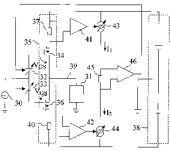
The invention will be further explained with reference to
fig. 3, that schematically shows a first embodiment of an
amplifier in accordance with the invention, an input signal
generator 30 connected to an input of the amplifier and a
load 31 connected to an output of the amplifier.
A first terminal of the input signal generator 30 is
connected to ground. A second terminal of the input signal
generator 30 is connected to a negative terminal of a first
programmable constant voltage generator 32 of a biasing stage
and to a positive terminal of a second programmable constant
voltage generator 33 of the biasing stage. A positive
terminal of the first voltage generator 32 is connected to a
gate terminal of an N-channel FET 34 residing in an OPS 35. A
negative terminal of the second voltage generator 33 is
connected to a gate terminal of a P-channel FET 36 also
residing in the OPS. A sourcing current sense resistor 37
within the OPS 35 has a first terminal that is connected to a
positive terminal of a power supply 38. A second terminal of
the sourcing current sense resistor 37 is connected to a
drain terminal of the N-channel FET 34. A source terminal of
the N-channel FET 34 is connected directly to an output node
39. The output node 39 is connected to a first terminal of
18
CA 02555960 2006-08-10
WO 2005/078918 PCT/SE2005/000197
the load 31. A second terminal of the load 31 is connected to
ground. The output node 39 is also connected directly to a
source terminal of the P-channel FET 36. A drain terminal of
the P-channel FET 36 is connected to a first terminal of a
sinking current sense resistor 40 within the OPS 35. A second
terminal of the sinking current sense resistor 40 is
connected to a negative terminal of the power supply 38. A
voltage mid-point terminal of the power supply 38 is
connected to ground.
Furthermore, the first and the second terminal of the
sourcing current sense resistor 37 are connected to a
respective input of an amplifier 41 of a sourcing current
sensing circuitry. The first and the second terminal of the
sinking current sense resistor 40 are connected to a
respective input of an amplifier 42 of a sinking current
sensing circuitry. An output of the sourcing current sensing
circuitry is connected to a control input of a sourcing
programmable constant-current generator 43. An output of the
sinking current sensing circuitry is connected to a control
input of a sinking programmable constant-current generator
44. A supply terminal of the sourcing current generator 43 is
connected to the positive terminal of the power supply 38. A
current source terminal of the sourcing current generator 43
is connected to a first terminal of a least current
determining resistor 45. A second terminal of the least
current determining resistor 45 is connected to a current
sink terminal of the sinking current generator 44. A supply
terminal of the sinking current generator 44 is connected to
the negative terminal of the power supply 38. The first and
the second terminals of the least current determining
resistor 45 are connected to a least current determining
differential amplifier 46. An output of the least current
determining differential amplifier 46 is connected to a
19
CA 02555960 2006-08-10
WO 2005/078918 PCT/SE2005/000197
respective control input of the first voltage generator 32
and to the second voltage generator 33 of the biasing stage.
The input signal generator 30 represents e.g. a VAS.
Programmable DC offsets are accomplished by means of the
programmable constant-voltage generators 32,33 that
constitute part of a biasing circuitry. The output signal
from the input signal generator 30 is voltage level-shifted
and separated into a first and a second control signal for
controlling the N-channel FET 34 and the P-channel FET 36
respectively. The N-channel FET 34 and the P-channel FET 36
are power handling active output devices that carry a load
current.
Current sensing circuitry is arranged for producing a first
control current and a second control current. The current
sensing circuitry senses a first voltage across the sourcing
current sense resistor 37, and in response thereto feeds a
control signal to a control input of the sourcing
programmable constant-current generator 43. Moreover, the
current sensing circuitry senses a second voltage across the
sinking current sense resistor 40, and in response thereto
feeds a control signal to a control input of the sinking
programmable constant-current generator 44.
The sourcing current generator 43 produces a first current Il
and the sinking current generator 44 produces a second
current I2. When the current generators 43,44 operate in
their linear, non-saturated region, the first and second
currents produced are proportional to the respective currents
through the sourcing circuitry and the sinking circuitry of
the OPS. This is the case when the first current equals the
second current, i.e. when there is no current through the
load 31.
CA 02555960 2006-08-10
WO 2005/078918 PCT/SE2005/000197
The sourcing current generator 43 sources the first current
I1 to a first terminal of a least current determining
resistor 45, and the sinking current generator 44 sinks the
second current I2 from a second terminal of the least current
determining resistor 45. The voltage across the least current
determining resistor 45 represents a current through the
least current determining resistor 45, which current is equal
to the least one of the current through the sourcing
circuitry and the current through the sinking circuitry of
the 0PS 35.
This is so because the current going into the least current
determining resistor 45 is equal to the current going out
from the least current determining resistor 45. Consequently,
the one of the current generator 43 or the current generator
44 attempting to source or sink a current being the larger
one is saturated.
As a consequence, the least one of the current through the
sourcing_,circuitry and the current through the sinking
circuitry of the OPS 35 becomes determinative of the current
through the least current determining resistor 45. A voltage
across the least current determining resistor 45 is thus a
proportional representation of the least one of the current
through the soureing circuitry and the current through the
sinking circuitry of the OPS 35.
The quiescent current is controlled through a negative
feedback loop in response to the voltage across the least
current determining resistor 45, which voltage thus further
represents the quiescent current. In more detail, the voltage
across the least current determining resistor 45 is sensed
through the least current determining differential amplifier
46. The least current determining differential amplifier 46
feeds a signal representing the least current to the
21
CA 02555960 2006-08-10
WO 2005/078918 PCT/SE2005/000197
programmable constant-voltage generator 32 and to the
programmable constant-voltage generator 33. An increase of
the voltage across the least ourrent determining resistor 45
results in a signal from the least current determining
differential amplifier 46 being such that the biasing
voltages aoross both programmable constant-voltage generators
32,33 decrease and vice versa.
It is to be particularly noted that the current sense
resistors 37,40 are not degeneration resistors. There are no
degeneration resistors in the output stage 35 for the output
transistors 34,36.
A change of load current or quiescent current is not
counteracted by means of local feedback since an associated
change of voltage across a current sense resistor 37,40 does
not yield a direct and passively induced change of control
voltage VGS.
Moreover, the bias voltages are equal. Bias regulation is
thus symmetric, which is advantageous with respect to
distortion.
The invention will now be further explained with reference to
fig. 4, that shows an embodiment in closer detail. An input
signal generator 50 has a first terminal connected to ground,
and a second terminal connected to a first terminal of a
sourcing bias voltage resistor 51 and to a first terminal of
a sinking bias voltage resistor 52. A second terminal of the
sourcing bias voltage resistor 51 is connected to a collector
terminal of a PNP-transistor 53 and to a gate terminal of an
N-channel FET 54. A base terminal of the PNP-transistor 53 is
connected to a negative terminal of a voltage source 55. A
positive terminal of the voltage source 55 is connected to a
positive terminal of a first supplementary voltage supply 56.
An emitter terminal of the PNP-transistor 53 is connected to
22
CA 02555960 2006-08-10
WO 2005/078918 PCT/SE2005/000197
a first terminal of a resistor 57. A second terminal of the
resistor 57 is connected to an emitter terminal of an NPN-
transistor 58. A collector terminal of the NPN-transistor 58
is connected to the positive terminal of the first
supplementary voltage supply 56. A drain terminal of the N-
channel FET 54 is connected to a first terminal of a sourcing
current sense resistor 59 and to a first terminal of a
resistor 60. A second terminal of the sourcing current sense
resistor 59 is connected to a positive terminal of a sourcing
voltage supply 61 and to a negative terminal of the first
supplementary voltage supply 56. A second terminal of the
resistor 60 is connected to a collector terminal of a PNP-
transistor 62 and to a base terminal of an NPN-transistor 63.
An emitter terminal of the PNP-transistor 62 is connected to
a first terminal of a resistor 64. A second terminal of the
resistor 64 is connected to the positive terminal of the
first supplementary voltage supply 56. An emitter terminal of
the NPN-transistor 63 is connected to a first terminal of a
resistor 65. A collector terminal of the NPN-transistor 63 is
connected to a first terminal of a resistor 66. A second
terminal of the resistor 65 is connected to a first terminal
of a constant current generator 67 and to a first terminal of
a resistor 68. A second terminal of the constant current
generator 67 is connected to ground. A second terminal of the
resistor 68 is connected to an emitter terminal of an NPN-
transistor 69. A collector terminal of the NPN-transistor 69
is connected to a first terminal of a resistor 70 and to a
base terminal of a PNP-transistor 71. A second terminal of
the resistor 70 is connected to the positive terminal of the
first supplementary voltage supply 56. An emitter terminal of
the PNP-transistor 71 is connected to a base terminal of the
PNP-transistor 62 and to a first terminal of a resistor 72. A
second terminal of the resistor 72 is connected to the
positive terminal of the first supplementary voltage supply
23
CA 02555960 2006-08-10
WO 2005/078918 PCT/SE2005/000197
56. A collector terminal of the PNP-transistor 71 is
connected to a base terminal of an NPN-transistor 73 and to a
first terminal of a resistor 74. A collector terminal of the
NPN-transistor 73 is connected to a first terminal of a
resistor 75 and to a base terminal of the NPN-transistor 58.
A second terminal of the resistor 75 is connected to the
positive terminal of the first supplementary voltage supply
56. An emitter terminal of the NPN-transistor 73 is connected
to a first terminal of a resistor 76. A negative terminal of
the sourcing voltage supply 61 is connected to ground.
Furthermore, a second terminal of the sinking bias voltage
resistor 52 is connected to a collector terminal of an NPN-
transistor 90 and to a gate terminal of a P-channel FET 91. A
base terminal of the NPN-transistor 90 is connected to a
positive terminal of a voltage source 92. A negative terminal
of the voltage source 92 is connected to a negative terminal
of a second supplementary voltage supply 93. An emitter
terminal of the NPN-transistor 90 is connected to a first
terminal of a resistor 94. A second terminal of the resistor
94 is connected to an emitter terminal of a PNP-transistor
95. A collector terminal of the PNP-transistor 95 is
connected to the negative terminal of the second
supplementary voltage supply 93. A drain terminal of the P-
channel FET 91 is connected to a first terminal of a sinking
current sense resistor 96 and to a first terminal of a
resistor 97. A second terminal of the sinking current sense
resistor 96 is connected to a negative terminal of a sinking
voltage supply 98 and to a positive terminal of the second
supplementary voltage supply 93. A second terminal of the
resistor 97 is connected to a collector terminal of an NPN-
transistor 99 and to a base terminal of a PNP-transistor 100.
An emitter terminal of the PNP-transistor 99 is connected to
a first terminal of a resistor 101. A second terminal of the
24
CA 02555960 2006-08-10
WO 2005/078918 PCT/SE2005/000197
resistor 101 is connected to the negative terminal of the
second supplementary voltage supply 93. An emitter terminal
of the PNP-transistor 100 is connected to a first terminal of
a resistor 102. A collector terminal of the PNP-transistor
100 is connected to a first terminal of a resistor 103. A
second terminal of the resistor 102 is connected to a first
terminal of a constant current generator 104 and to a first
terminal of a resistor 105. A second terminal of the constant
current generator 104 is connected to ground. A second
terminal of the resistor 105 is connected to an emitter
terminal of a PNP-transistor 106. A collector terminal of the
PNP-transistor 106 is connected to a first terminal of a
resistor 107 and to a base terminal of a NPN-transistor 108.
A second terminal of the resistor 107 is connected to the
negative terminal of the second supplementary voltage supply
93. An emitter terminal of the NPN-transistor 108 is
connected to a base terminal of the NPN-transistor 99 and to
a first terminal of a resistor 109. A second terminal of the
resistor 109 is connected to the negative terminal of the
second supplementary voltage supply 93. A collector terminal
of the NPN-transistor 108 is connected to a base terminal of
a PNP-transistor 110 and to a second terminal of the resistor
74. A collector terminal of the PNP-transistor 110 is
connected to a first terminal of a resistor 111 and to a base
terminal of the PNP-transistor 95. A second terminal of the
resistor 111 is connected to the negative terminal of the
second supplementary voltage supply 93. An emitter terminal
of the PNP-transistor 110 is connected to the second terminal
of the resistor 76. A source terminal of the N-channel FET 54
and the P-channel FET 91 respectively are connected to a
first terminal of a load 112. A second terminal of the load
is connected to ground. A positive terminal of the sinking
voltage supply 98 is connected to ground.
CA 02555960 2006-08-10
WO 2005/078918 PCT/SE2005/000197
The sourcing current sense resistor 59, the sinking current
sense resistor 96, the N-channel FET 54 and the P-channel FET
91 constitute a source-follower, i.e. CC-type OPS, where the
N-channel FET 54 and the P-channel FET 91 are active output
devices. Sensing of a sourcing current ID1 through the N-
channel FET 54 and a sinking current IDZ through the P-
channel FET 91 is accomplished by sensing a respective
voltage across the sourcing current sense resistor 59 and the
sinking current sense resistor 96.
Voltage sensing in turn is accomplished by a respective so-
called long-tailed-pair. The first long-tailed pair includes
the transistor 63, the transistor 69, the resistor 65, the
resistor 68, the constant current generator 67, the resistor
66 and the resistor 70. The second long-tailed pair includes
the transistor 100, the transistor 106, the resistor 102, the
resistor 105, the constant current generator 104, the
resistor 103 and the resistor 107. In the current embodiment,
a respective resistor is a good approximation of said
constant current generators 67,104.
The long-tailed pairs are included in a respective
differential amplifier. The first differential amplifier also
contains the transistor 71 and the resistor 72, and the
second differential amplifier also contains the transistor
108 and the resistor 109. The transistor 71 and the resistor
72 produce a constant current IC1 in response to a
differential voltage applied across inputs of the first
differential amplifier, and the transistor 108 and the
resistor 109 produce a constant current I~2 in response to a
differential voltage applied across inputs of the second
differential amplifier. The inputs are applied across the
respective current sense resistors 59,96, via resistors 60,
97. The function of the resistors 60,97 will now be
explained.
26
CA 02555960 2006-08-10
WO 2005/078918 PCT/SE2005/000197
The constant current Ici constitutes an output signal of the
first differential amplifier and IC2 constitutes an output
signal of the second differential amplifier.
The transistor 62, the resistor 64 and the resistor 60 are
arranged to provide negative feedback on the current ICi
produced at the output of the first differential amplifier. A
voltage is sensed across the resistor 72, which voltage
represents the current Icl, and a proportional voltage is
produced across the resistor 60, thus causing negative
feedback.
Conversely, the transistor 99, the resistor 101 and the
resistor 97 are arranged to provide negative feedback on the
current Ic2 produced at the output of the second differential
amplifier. A voltage is sensed across the resistor 109, which
voltage represents the current Ic2, and a proportional
voltage is produced across the resistor 97, thus causing
negative feedback.
The negative feedback arrangement just discussed reduces
effects of process variations, i.e. parameter variations
between components caused by manufacturing tolerances, and
thermal variations. As a result, the currents Ic1 and Ica
become highly accurate.
The current Ic1 is a proportional representation of the
current ID1, provided the transistor 71 operates in its
linear operating range, while the current Ic2 is a
proportional representation of the current ID2, provided the
transistor 108 operates in its linear operating range.
However, the transistor 71 sources a current Icl into the
resistor 74, and the transistor 107 sinks a current Ic2 from
the resistor 74. It follows from Kirchoff's Current Law,
stating that the algebraic sum of currents entering or
27
CA 02555960 2006-08-10
WO 2005/078918 PCT/SE2005/000197
leaving a node must equal zero, that in the presence of a
load current, either the transistor 71 has a larger current
sourcing capability than the current sinking capability of
the transistor 108, or the transistor 108 has a larger
current sinking capability than the current sourcing
capability of the transistor 71. Consequently, either the
transistor 71 saturates, or the transistor 108 saturates.
Accordingly, a current IC1 or I~2 will not represent a larger
one of the currents ID1 or ID2, but will be recessed so that
the currents ICi and I~~ become substantially equal. The
currents ICZ and ICZ as a result are both representative of
the smaller one of the currents IDi and ID2, i.e. the
quiescent current. Consequently, the voltage across the
resistor 74 represents the quiescent current.
A differential amplifying circuit containing the transistor
73, the transistor 110, the resistor 76, the resistor 75 and
the resistor 111 amplifies the voltage across the resistor
74. A first and a second output from the differential
amplifying circuit controls a respective programmable
constant current generator, one of which consists of the
transistor 58, the resistor 57 and the transistor 53 and the
voltage source 55, and the other one consisting of the
transistor 95, the resistor 94 and the transistor 90 and the
voltage source 92.
Currents produced by the programmable constant current
generators generate a respective voltage across the resistors
51,52. These voltages are bias voltages. The bias voltages
determine the quiescent current, while a voltage of the input
signal generator 50 substantially determines a voltage at the
load 112, i.e. at the output of the OPS.
The input signals of the OPS are a respective OPS control
voltage applied to the gate terminals of the active output
28
CA 02555960 2006-08-10
WO 2005/078918 PCT/SE2005/000197
devices 54,91. Since the OPS is a basic source follower, the
OPS control voltages are referenced to the voltage at the
output of the OPS. Because of the absence of degeneration
resistors, an OPS control voltage and a voltage VGS between
the gate terminal and the source terminal of the related
active output device are one and the same, regardless of load
current.
Therefore, the OPS departs from unity voltage gain in the
presence of a load current only as determined by the finite
transconductance of the active output devices.
Transconductance is the change of drain current ID brought
about by a (one volt) change of voltage VGS between the gate
terminal and the source terminal of an output transistor.
Provided the transconductance is sufficiently large, the
amplifier is thus substantially load-invariant, i.e. the
output voltage is substantially unaffected by varying load
impedance.
The input signal generator 50 typically represents an input
stage and a VAS. The currents of the programmable constant
current generators are substantially equal. Accordingly, the
constant current generators do not constitute a load on the
input signal generator 50.
Furthermore, voltages across the resistor 51 and the resistor
52 are equal and the overall circuitry is arranged in a way
such that bias control affects both the sourcing active
output device, i.e. the N-channel FET 54, and the sinking
active output device, i.e. the P-channel FET 91, equally.
Biasing is thus symmetric.
The invention will now be further explained with reference to
fig. 5, which shows another embodiment of the invention. An
input signal generator 120 has a first terminal connected to
29
CA 02555960 2006-08-10
WO 2005/078918 PCT/SE2005/000197
ground. A second terminal of the input signal generator 120
is connected to a base terminal of an NPN-transistor 121. A
collector terminal of the NPN-transistor 121 is connected to
a first terminal of a resistor 122 and to a base terminal of
a PNP-transistor 123. A second terminal of the resistor 122
is connected to a positive terminal of a first supplementary
voltage supply 124. An emitter terminal of the NPN-transistor
121 is connected to a first terminal of a resistor 125. A
second terminal of the resistor 125 is connected to a first
terminal of a current generator 126 and to a first terminal
of a resistor 127. A second terminal of the resistor 127 is
connected to an emitter terminal of an NPN-transistor 128. A
collector terminal of the NPN-transistor 128 is connected to
a first terminal of a resistor 129. A second terminal of the
resistor 129 is connected to the first supplementary voltage
supply 124. A second terminal of the current generator 126 is
connected to a second supplementary voltage supply 130. A
base terminal of the NPN-transistor 128 is connected to a
first terminal of a resistor 131 and to a first terminal of a
resistor 132. A second terminal of the resistor 132 is
connected to a first terminal of a load 133. A second
terminal of the load 133 is connected to ground. A base
terminal of the PNP-transistor 123 is connected to a first
terminal of a resistor 134. A collector terminal of the PNP-
transistor 123 is connected to a base terminal of an NPN-
transistor 135 and to an anode terminal of a diode 136. A
cathode terminal of the diode 136 is connected to an anode
terminal of a diode 137. A cathode terminal of the diode 137
is connected to an anode terminal of a diode 138. A cathode
terminal of the diode 138 is connected to an emitter terminal
of a PNP-transistor 139. A collector terminal of the PNP-
transistor 139 is connected to a first terminal of a current
generator 140. A second terminal of the current generator 140
is connected to the negative terminal of the second
CA 02555960 2006-08-10
WO 2005/078918 PCT/SE2005/000197
supplementary voltage supply 130. A base terminal of the PNP-
transistor 139 is connected to the collector terminal of the
PNP-transistor 139 and to a base terminal of a PNP-transistor
141.
An emitter terminal of the NPN-transistor 135 is connected to
a first terminal of a resistor 150. A second terminal of the
resistor 150 is connected to the first terminal of the load
133. A collector terminal of the NPN-transistor 135 is
connected to a first terminal of a resistor 151 and to a base
terminal of a PNP-transistor 152. A collector terminal of the
PNP-transistor 141 is connected to the negative terminal of
the second supplementary voltage supply 130. An emitter
terminal of the PNP-transistor 141 is connected to a first
terminal of a resistor 153. A second terminal of the resistor
153 is connected to an emitter terminal of an NPN-transistor
154. A base terminal of the NPN-transistor 154 is connected
to the first terminal of the load 133. A collector terminal
of the NPN-transistor 154 is connected to a first terminal of
a resistor 155 and to a base terminal of a PNP-transistor
156. A second terminal of the resistor 151 and a second
terminal of the resistor 155 are connected to an emitter
terminal of an NPN-transistor 157 and to a first terminal of
a resistor 158. A second terminal of the resistor 158 is
connected to a first terminal of a potentiometer 159. A wiper
terminal of the potentiometer 159 is connected to a base
terminal of the NPN-transistor 157. A second terminal of the
potentiometer 159 is connected to a first terminal of a
resistor 160. A second terminal of the resistor 160 is
connected to the positive terminal of the first supplementary
voltage supply 124. A collector terminal of the NPN-
transistor 157 is connected to the positive terminal of the
first supplementary voltage supply 124.
31
CA 02555960 2006-08-10
WO 2005/078918 PCT/SE2005/000197
An emitter terminal of the PNP-transistor 156 is connected to
a first terminal of a resistor 161. An emitter terminal of
the PNP-transistor 152 is connected to a first terminal of a
resistor 162. A second terminal of the resistor 161 and a
second terminal of the resistor 162 are connected to an
emitter terminal of an NPN-transistor 163. A collector
terminal of the NPN-transistor 163 is connected to the
positive terminal of the first supplementary voltage supply
124. A collector terminal of the PNP-transistor 156 is
connected to a base terminal of an NPN-transistor 170 and to
an anode terminal of a diode 171. A cathode terminal of the
diode 171 is connected to an anode terminal of a diode 172. A
cathode terminal of the diode 172 is connected to an anode
terminal of a diode 173. A cathode terminal of the diode 173
is connected to a first terminal of a resistor 174 and to a
base terminal of a PNP-transistor 175. A second terminal of
the resistor 174 is connected to a first terminal of a
current sense resistor 176.
A collector terminal of the PNP-transistor 152 is connected
to an anode terminal of a diode 177 and to a base terminal of
an NPN-transistor 178. A cathode terminal of the diode 177 is
connected to an anode terminal of a diode 179. A cathode
terminal of the diode 179 is connected to an anode terminal
of a diode 180. A cathode terminal of the diode 180 is
connected to a first terminal of a resistor 181 and to a base
terminal of a PNP-transistor 182. A second terminal of the
resistor 181 is connected to the first terminal of the load
133. A collector terminal of the NPN-transistor 178 is
connected to a positive terminal of a third supplementary
voltage supply 183. An emitter terminal of the NPN-transistor
178 is connected to a first terminal of a resistor 184. A
second terminal of the resistor 184 is connected to a gate
terminal of a first N-channel FET 185 and to a first terminal
32
CA 02555960 2006-08-10
WO 2005/078918 PCT/SE2005/000197
of a resistor 186. A second terminal of the resistor 186 is
connected to an emitter terminal of the PNP-transistor 182. A
collector terminal of the PNP-transistor 182 is connected to
the first terminal of the load 133. A negative terminal of
the third supplementary voltage supply 183 is connected to
the first terminal of the load 133. A collector terminal of
the NPN-transistor 170 is connected to a positive terminal of
a fourth supplementary voltage supply 187. An emitter
terminal of the NPN-transistor 170 is connected to a first
terminal of a resistor 188. A second terminal of the resistor
188 is connected to a gate terminal of a second N-channel FET
189 and to a first terminal of a resistor 190. A second
terminal of the resistor 190 is connected to a base terminal
of the PNP-transistor 175. A negative terminal of the fourth
supplementary voltage supply 187 is connected to the first
terminal of the current sense resistor 176. A negative
terminal of the first supplementary voltage supply 124 is
connected to a positive terminal of a positive power supply
191. A positive terminal of the second supplementary voltage
supply 130 is connected to a negative terminal of a negative
power supply 192. A negative terminal of the positive power
supply 191 and a positive terminal of the negative power
supply 192 are connected to ground.
Moreover, a source terminal of the first N-channel FET 185 is
connected to the first terminal of the load 133 and to a
drain terminal of the second N-channel FET 189. A drain
terminal of the first N-channel FET 185 is connected to a
first terminal of a current sense resistor 200 and to a first
terminal of a resistor 201. A second terminal of the current
sense resistor 200 is connected to the positive terminal of
the positive power supply 191. A second terminal of the
resistor 201 is connected to a base terminal of an NPN-
transistor 202 and to a collector terminal of a PNP-
33
CA 02555960 2006-08-10
WO 2005/078918 PCT/SE2005/000197
transistor 203. An emitter terminal of the PNP-transistor 203
is connected to a resistor 204. A second terminal of the
resistor 204 is connected to the positive terminal of the
first supplementary voltage supply 124. A collector terminal
of the PNP-transistor 202 is connected to a first terminal of
a resistor 205. A second terminal of the resistor 205 is
connected to the positive terminal of the first supplementary
voltage supply 124. An emitter terminal of the NPN-transistor
202 is connected to a first terminal of a resistor 206. A
second terminal of the resistor 206 is connected to a first
terminal of a third current generator 207 and to a first
terminal of a resistor 208. A second terminal of the resistor
208 is connected to an emitter terminal of an NPN-transistor
209. A collector terminal of the NPN-transistor 209 is
connected to a base terminal of a PNP-transistor 210 and to a
first terminal of a resistor 211. A second terminal of the
resistor 211 is connected to the positive terminal of the
first supplementary voltage supply 124. A base terminal of
the NPN-transistor 209 is connected to the positive terminal
of the positive power supply 191. A second terminal of the
current generator 207 is connected to ground.
A source terminal of the second N-channel FET 189 is
connected to the first terminal of the current sense resistor
176 and to a first terminal of a resistor 212. A second
terminal of the resistor 212 is connected to a base terminal
of a PNP-transistor 213 and to a collector terminal of an
NPN-transistor 214. An emitter terminal of the transistor 214
is connected to a first terminal of a resistor 215. A second
terminal of the resistor 215 is connected to the negative
terminal of the second supplementary voltage supply 130. A
collector terminal of the PNP-transistor 213 is connected to
a first terminal of a resistor 216. A second terminal of the
resistor 216 is connected to the negative terminal of the
34
CA 02555960 2006-08-10
WO 2005/078918 PCT/SE2005/000197
second supplementary voltage supply 130. An emitter terminal
of the PNP-transistor 213 is connected to a first terminal of
a resistor 217. A second terminal of the resistor 217 is
connected to a fourth constant current generator 218 and to a
first terminal of a resistor 219. A second terminal of the
resistor 219 is connected to an emitter terminal of a PNP-
transistor 220. A collector terminal of the PNP-transistor
220 is connected to a base terminal of an NPN-transistor 221
and to a first terminal of a'resistor 222. A second terminal
of the resistor 222 is connected to the negative terminal of
the second supplementary voltage supply 130. A base terminal
of. the PNP-transistor 220 is connected to the negative
terminal of the negative power supply 192. A second terminal
of the fourth constant current generator 218 is connected to
ground.
An emitter terminal of the PNP-transistor 210 is connected to
a first terminal of a resistor 223 and to a base terminal of
the PNP-transistor 203. A second terminal of the resistor 223
is connected to the positive terminal of the first
supplementary voltage supply 124. A collector terminal of the
PNP-transistor 210 is connected to a first terminal of a
resistor 224 and to a base terminal of an NPN-transistor 225.
A second terminal of the resistor 224 is connected to a base
terminal of a PNP-transistor 226 and to a collector terminal
of the NPN-transistor 221. An emitter terminal of the
transistor 221 is connected to a base terminal of the NPN-
transistor 214 and to a first terminal of a resistor 227. A
second terminal of the resistor 227 is connected to the
negative terminal of the second supplementary voltage supply
130. A first terminal of a resistor 228 is connected to the
positive terminal of the supplementary voltage supply 124. A
second terminal of the resistor 228 is connected to a base
terminal of the NPN-transistor 163 and to a collector
CA 02555960 2006-08-10
WO 2005/078918 PCT/SE2005/000197
terminal of the NPN-transistor 225. An emitter terminal of
the NPN-transistor 225 is connected to a first terminal of a
resistor 229. A second terminal of the resistor 229 is
connected to an emitter terminal of the PNP-transistor 226. A
collector of the PNP-transistor 226 is connected to the
negative terminal of the second supplementary voltage supply
130.
The signal generator 120 generates a signal representative of
a low level signal to be amplified by the amplifier. The
signal enters at a positive differential input of a
differential input stage, at the base terminal of the NPN-
transistor 121. The input stage further accommodates the NPN-
transistor 128, the resistor 125, the resistor 127, the
resistor 122, the resistor 129 and the constant current
generator 126. The base terminal of the NPN-transistor 128
constitutes a negative differential input of the differential
input stage. The input stage is a first long-tailed pair of
the amplifier.
The output of the first long-tailed pair is connected to a
VAS. The VAS consists of the resistor 134, the PNP-transistor
123, the diode 136, the diode 137, the diode 138, the PNP-
transistor 139, and the constant current generator 140. The
VAS has two outputs with a reciprocal voltage difference
determined by the aggregated voltage drop across the diodes
136,137,138 and the PNP-transistor 139.
The current sense resistor 200, the current sense resistor
176, the first N-channel FET 185 and the second N-channel FET
189 form a quasi-complementary OPS, where the first N-channel
FET 185 and the second N-channel FET 189 are thus active
output devices for sourcing and sinking current respectively.
Henceforth, these are referred to as sourcing FET 185 and
sinking FET 189 respectively. An output of the OPS
36
CA 02555960 2006-08-10
WO 2005/078918 PCT/SE2005/000197
constitutes the output of the amplifier, the output of which
is connectable to a load 133 such as e.g. a loudspeaker.
The one output of the VAS that is positive relative to the
other is fed to an input of a sourcing drive circuit whose
output is fed to the gate terminal of the sourcing FET 185.
The circuit comprises the resistor 151, the NPN-transistor
135, the resistor 150, the resistor 162, the PNP-transistor
152, the diode 177, the diode 179, the diode 180, the
resistor 181, the NPN-transistor 178, the resistor 184, the
resistor 186, the PNP-transistor 182 and the third
supplementary voltage supply 183.
The input signal of the sourcing drive circuit to which the
VAS is connected is a voltage applied between the base
terminal of the NPN-transistor 135 and the output of the
amplifier. The input signal from the VAS is thus referenced
directly to the output node of the OPS. The sourcing drive
circuit provides an output signal having a voltage gain
relative to the source terminal of the first FET 185, e.g.
unity gain. The output signal of the sourcing drive circuit
is a voltage VGS applied directly between the gate terminal
and the source terminal of the sourcing FET 185.
The circuit has two additional inputs. These are for bias
voltage control. A circuit comprising the resistor 160, the
potentiometer 159, the resistor 158 and the NPN-transistor
157 constitute a voltage source whose output is fed to a
first one of said two additional inputs. The voltage source
provides a programmable but substantially static control
voltage for controlling the bias voltage of the sourcing FET
185, and in turn controlling the quiescent current of the
OPS. The voltage is referenced to the positive terminal of
the first supplementary voltage supply 124. The second one of
37
CA 02555960 2006-08-10
WO 2005/078918 PCT/SE2005/000197
said two additional inputs is fed from a voltage provided at
the emitter terminal of the NPN-transistor 163.
The one output of the VAS that is negative relative to the
other is fed to an input of a sinking drive circuit whose
output is fed to the gate terminal of the sinking FET 189.
The circuit comprises the PNP-transistor 141, the resistor
153, the NPN-transistor 154, the resistor 155, the resistor
161, the PNP-transistor 156, the diode 171, the diode 172,
the diode 173, the resistor 174, the NPN-transistor 170, the
resistor 188, the resistor 190, the PNP-transistor 175 and
the fourth supplementary voltage supply 187.
The sinking drive circuit is similar in function to the
sourcing drive circuit, but the output of the sinking drive
circuit is referenced to the source terminal of the sinking
FET 189 rather than the source terminal of the sourcing FET
185. The input signal is a voltage applied between the base
terminal of the transistor 141 and the output of the
amplifier. The input signal from the VAS is thus referenced
directly to the output node of the OPS. The gain is
substantially the same as the gain of the sourcing drive
circuit, although negative. The sinking drive circuit thus
inverts a signal at its input. The output signal of the
sinking drive circuit is a voltage VAS applied directly
between the gate terminal and the source terminal of the
sinking FET 189.
The sinking drive circuit also has two additional inputs for
bias voltage control, connected in the same fashion as the
two additional inputs of the sourcing drive circuit.
Accordingly, the output of the aforementioned voltage source
is fed to a first one of said two additional inputs of the
sinking drive circuit, for controlling the bias voltage of
the sinking FET 189, and in turn controlling the quiescent
38
CA 02555960 2006-08-10
WO 2005/078918 PCT/SE2005/000197
current of the OPS. The second one of said two additional
inputs of the sinking drive circuit is fed from the voltage
provided at the emitter terminal of the NPN-transistor 163.
The sourcing drive circuit and the sinking drive circuit can
be viewed as comprising current mirrors whose DC operating
point is programmable by means of applying voltages at the
bias voltage control inputs. A voltage applied at the second
terminal of the resistor 155 and to the second terminal of
the resistor 151 typically controls a substantially static
biasing, while a voltage applied to the second terminal of
the resistor 161 and to the second terminal of the resistor
162 controls a dynamic biasing. A differential mode voltage
applied across the bias voltage control inputs gives rise to
a respective bias voltage applied between the gate and source
terminals of the sourcing and sinking active output devices
185,189. The bias voltages are substantially equal.
Currents through the sourcing FET 185 and the sinking FET 189
are determined by sensing a respective voltage across the
current sense resistors 200,176. The base terminals of the
NPN-transistors 202,209 are inputs for measuring the voltage
across the current sense resistor 200, via the resistor 201.
The NPN-transistors 202,209 are members of a second long-
tailed pair of a second differential amplifier for amplifying
the voltage across the current sense resistor 200, and
converting it to a sourcing sense current IC1 being sourced
to the resistor 224. Said long-tailed pair further
encompasses the constant current generator 207. In the
embodiment shown, a good approximation of the constant
current generator 207 is a resistor.
Conversely, the base terminals of the PNP-transistors 213,
220 are inputs for measuring the voltage across the current
sense resistor 176, via the resistor 212. The PNP-transistors
39
CA 02555960 2006-08-10
WO 2005/078918 PCT/SE2005/000197
213,220 are members of a third long-tailed pair of a third
differential amplifier for amplifying the voltage across the
current sense resistor 176, and sinking a sinking sense
current I~~ from the resistor 224. Said long-tailed pair
further encompasses the constant current generator 218. In
the embodiment shown, a good approximation of the constant
current generator 218 is a resistor.
A voltage across the resistor 224 is sensed and a
proportional voltage being referenced to the positive
terminal of the first supplementary voltage supply 124 is
applied at the base terminal of the NPN-transistor 163. The
NPN-transistor 163 operates as an emitter-follower. Hence, a
voltage proportional to the voltage across the resistor 224
is present between the emitter terminal of the NPN-transistor
163 and the positive terminal of the first supplementary
voltage supply 124.
Accordingly, an increase of the aforesaid programmable but
substantially static control voltage for controlling the bias
voltages results in an increase of gate voltages VGS of the
active output devices, and consequently an increase of the
quiescent current, and vice versa.
Furthermore, an increase of the voltage between the positive
terminal of the first supplementary voltage supply 124 and
the emitter terminal of the NPN-transistor 163 results in
decreased gate voltages of the active output devices, and
vice versa.
The static control voltage is adjustable by means of the
potentiometer 159. By a slightly different opting, e.g. by
slightly increasing the impedance of the current sense
resistors 200,176, or by introducing temperature compensation
by means of e.g. a thermistor, not shown, a potential need
for trimming of individual amplifiers during production is
CA 02555960 2006-08-10
WO 2005/078918 PCT/SE2005/000197
obviated. Thus, the potentiometer 159 either is, or can be
made obsolete and replaced by a fixed resistor network.
Neither of the current sense resistors 200,176 are arranged
to passively control a respective voltage VAS applied between
the gate terminal and the source terminal of the sourcing FET
185 and the sinking FET 189 by means of local feedback.
It is to be particularly observed that although the current
sense resistor 176 is connected to the source terminal of the
sinking FET 189, it is not a degeneration resistor, since it
is indeed excluded from forming a local feedback loop. A
voltage drop across the current sense resistor 176 does not
directly yield a reduction of the voltage VGS applied between
the gate terminal and the source terminal of the sinking FET
189. Rather, the voltage VAS depends on the voltage across
the resistor 174 which in turn depends on the current
supplied from the transistor 156 and so forth.
A circuit containing the transistor 203, the resistor 204 and
the resistor 201, and a circuit containing the transistor
214, the resistor 215 and the resistor 212 provide feedback
in the same manner as in the embodiment of fig. 4, for
reducing effects of process and thermal variations, and thus
for providing highly accurate currents Icz and Ic2.
The amplifier furthermore employs global, overall negative
voltage feedback. A feedback network comprising the resistor
138 and the resistor 131 is arranged between the output of
the amplifier and the negative input of the aforementioned
first long-tailed pair, at the base terminal of the NPN-
transistor 128.
Compensation capacitors, not shown, may be added to increase
stability of the amplifier, e.g. a miller-type capacitance in
41
CA 02555960 2006-08-10
WO 2005/078918 PCT/SE2005/000197
the input stage of the amplifier in order to accomplish a
dominant pole. Compensation is well known in the art.
It should be appreciated that the OPS current-sense resistors
may be placed differently than shown, both for CC and CE
topologies and quasi-complementary designs, without departing
from the scope and the spirit of the invention. The important
aspect of the invention with respect to placement of current
sense resistors is that a voltage across a current sense
resistor placed in a sourcing or sinking current path of an
OPS, for sensing a current through the sourcing circuitry and
sinking circuitry respectively does not passively and
directly affect a control signal applied at the input of a
corresponding active output device.
This is typically accomplished by relating an OPS control
voltage applied to a gate terminal, base terminal or
equivalent of an active output device directly to the shared
terminal of the active output device, i.e. to the source
terminal, emitter terminal or equivalent.
The invention will now be explained further with reference to
the flow chart depicted in fig. 6.
A sourcing current in an OPS of a push-pull amplifier is
sensed by sensing a first voltage across a sourcing sense
resistor located in a sourcing current path of the OPS, S1.
Furthermore, a sinking current in the OPS is sensed by
sensing a second voltage across a sinking sense resistor
located in a sinking current path of the OPS, S2.
In response to the sensed first and second voltages that
represent the sourcing current and the sinking current
respectively, a current is produced, which current represents
the least one of the sourcing current and the sinking
current, S3.
42
CA 02555960 2006-08-10
WO 2005/078918 PCT/SE2005/000197
The current is drawn through a resistor, for producing a bias
control voltage proportional thereto. The bias control
voltage is sensed and in response thereto, a first and a
second bias voltage are established which control the
quiescent current of the amplifier. The first and second bias
voltages are inversely proportional to the bias control
voltage, for providing negative feedback, S4.
An output stage sourcing-signal is referenced directly to a
shared terminal of a corresponding sourcing active output
device, and an output stage sinking-signal is referenced
directly to a shared terminal of a corresponding sinking
active output device, S5.
The invention is applicable to a broad range of classes,
topologies and modes of operation not explicitly explained
herein. Any necessary alterations of the invention would be
obvious to one skilled in the art. The invention is for
example applicable to output power stages having cascoded or
paralleled active output devices. The active output devices
are typically FETs, e.g. vertical Power MOSFETs (DMOSFETs),
or BJTs but may also be e.g. valves or IGBTs.
43