Note: Descriptions are shown in the official language in which they were submitted.
CA 02556303 2006-08-16
- 1 -
TITLE OF THE INVENTION
PRINTED CIRCUIT BOARD FOR REAL-TIME CLOCK IC AND
MANUFACTURING METHOD FOR PRINTED CIRCUIT BOARD FOR
REAL-TIME CLOCK IC
BACKGROUND OF THE INVENTION
One embodiment of the invention relates to a
printed circuit board for a real-time clock IC used in
an electronic equipment such as a key-telephone
equipment, for example, and a manufacturing method for
the printed circuit board for the real-time clock IC.
Generally, a real time clock IC is used in an
electronic equipment such as a key-telephone equipment
to realize a real-time clock function. An oscillation
frequency of 32.768 KHz is generally used in the real
time clock IC and a tuning fork type crystal is used as
a crystal oscillator which oscillates at the above
frequency.
In the above electronic equipment, the
specification of an error of ~1 minute for each month
is required for the real time clock function as one
example. In order to satisfy the above required
specification, the precision of the oscillation
frequency of ~23 ppm is required. However, a variation
in the center value in a tuning fork type crystal is
large and an oscillation frequency change due to
temperatures occurs. Therefore, generally, one of
capacitors connected to both ends of the crystal
CA 02556303 2006-08-16
- 2 -
oscillator is formed as a trimmer capacitor and the
oscillation frequency is adjusted at the time of
product shipment.
The capacitances of the capacitors connected to
both ends of the crystal oscillator are generally as
small values as before and behind 10 pf(s). Therefore,
since the oscillation frequency is influenced by stray
capacitance or the like due to a pattern of the printed
circuit board, the capacitance of the capacitor on the
fixed-capacitance side is adjusted for each type so as
to extend the adjusting frequency range by the trimmer
capacitor into the center value of the target
oscillation frequency.
However, recently, the printed circuit board is
formed into a multiple layered form with an increase in
the density and a gap between the crystal oscillator
circuit pattern layer and the power supply layer or
ground layer becomes smaller, it cause to increase the
stray capacitance including at around crystal circuit.
In the worst case, there occurs a problem that the
adjusting range cannot be set into the target range of
the center value of the oscillation frequency on the
trimmer capacitor side even if the capacitance on the
fixed-capacitance side is set to 0.
Conventionally, there is provided a method for
collectively forming, arranging and wiring the crystal
oscillation circuit in one layer in the multi-layered
CA 02556303 2006-08-16
- 3 -
substrata structure and removing all of corresponding
portions of the other circuit patterns lying in the
vertical surface of the area at another layer (for
example, refer to Jpn. Pat. Appln. KOKAI Publication
No. H10-22734).
However, with the above method, since the crystal
oscillation circuit must be collectively formed,
arranged and wired in one layer, it takes a long time
and labor to manufacture the same. Further, it is
required to change the design of the circuit pattern
because a pattern extracting portion is provided for
each wiring layer and the manufacturing cost will be
raised.
BRIEF SUMMARY OF THE INVENTION
According to an aspect of the present invention,
there is provided a printed circuit board for a real-
time clock IC comprising: a plurality of wiring layers
sequentially laminated to form one substrata and
including at least one layer which forms an oscillator
circuit pattern having a crystal oscillator generating
a reference signal and an oscillation stabilizing
portion which stabilizes and oscillates the reference
signal and adjusts the oscillation frequency to a
target frequency, and a power supply layer arranged in
at least one of a position between the plurality of
wiring layers and a position on one of front and rear
surfaces of the substrate, and obtained by forming a
CA 02556303 2006-08-16
- 4 -
power supply circuit pattern which supplies electric
power to a circuit on the substrate and removing a
portion of the power supply circuit pattern which has
width not smaller than width of the oscillator circuit
pattern in a portion of the power supply circuit
pattern which overlaps with the oscillator circuit
pattern, when the surface of the substrata is projected
in a vertical direction at another layer.
According to another aspect of the present
invention, there is provided a printed circuit board
for a real-time clock IC comprising: a plurality of
wiring layers sequentially laminated to form one
substrate and including at least one layer which forms
an oscillator circuit pattern having a crystal
oscillator generating a reference signal and an
oscillation stabilizing portion which stabilizes and
oscillates the reference signal and adjusts the
oscillation frequency to a target frequency, and a
ground layer arranged in at least one of a position
between the plurality of wiring layers and a position
on one of front and rear surfaces of the substrata and
obtained by forming a ground circuit pattern which
lowers electric power from a circuit on the substrata
to ground power and removing a portion of the ground
circuit pattern which has width not smaller than width
of the oscillator circuit pattern in a portion of the
ground circuit pattern which overlaps with the
CA 02556303 2006-08-16
- 5 -
oscillator circuit pattern when the surface of the
substrata is projected in a vertical direction at
another layer.
According to yet another aspect of the present
invention, there is provided a manufacturing method for
a printed circuit board for a real-time clock IC which
includes a plurality of wiring layers sequentially
laminated to form one substrata and including at least
one of layer which forms an oscillator circuit pattern
having a crystal oscillator generating a reference
signal and an oscillation stabilizing portion which
stabilizes and oscillates the reference signal and
adjusts a oscillation frequency to a target frequency,
comprising: preparing at least one of a power supply
layer obtained by forming a power supply circuit
pattern which supplies electric power to a circuit on
the substrata and removing a portion of the power
supply circuit pattern which has width not smaller than
width of the oscillator circuit pattern in a portion of
the power supply circuit pattern which overlaps with
the oscillator circuit pattern when the surface of the
substrata is projected in a vertical direction and a
ground layer obtained by forming a ground circuit
pattern which lowers electric power from the circuit on
the substrate to ground power and removing a portion of
the ground circuit pattern which has width not smaller
than width of the oscillator circuit pattern in a
CA 02556303 2006-08-16
- 6 -
portion of the ground circuit pattern which overlaps
with the oscillator circuit pattern when the surface of
the substrata is projected in a vertical direction, and
arranging at Least one of the power supply layer and
ground layer in one of a position between the plurality
of wiring layers and a position on one of front and
rear surfaces of the substrata.
Additional objects and advantages of the invention
will be set forth in the description which follows, and
in part will be obvious from the description, or may be
learned by practice of the invention. The objects and
advantages of the invention may be realized and
obtained by means of the instrumentalities and
combinations particularly pointed out hereinafter.
BRIEF DESCRIPTION OF THE SEVERAL VIEWS OF THE DRAWING
A general architecture that implements the various
feature of the invention will now be described with
reference to the drawings. The drawings and the
associated descriptions are provided to illustrate
embodiments of the invention and not to limit the scope
of the invention.
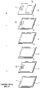
FIG. 1 is a perspective view showing the laminated
structure of a printed circuit board for a real-time
clock IC according to one embodiment of this invention.
FIG. 2 is a plan view of the printed circuit board
for a real-time clock IC as viewed from the side in the
above embodiment.
CA 02556303 2006-08-16
FIG. 3A is a plan view of the wiring layer of the
printed circuit board for a real-time clock IC as
viewed from above in the above embodiment.
FIG. 3B is a plan view of the power supply layer
of the printed circuit board for a real-time clock IC
as viewed from above in the above embodiment.
FIG. 4 is a circuit diagram showing one example of
the connection configuration of an oscillator circuit
pattern and a real-time clock IC in the above
embodiment.
FIG. 5 is a circuit diagram for illustrating the
relation between the adjusting capacitance and stray
capacitance in the above embodiment.
FIG. 6 is a block diagram when the printed circuit
board for a real-time clock IC according to the above
embodiment is applied to a timer of a key-telephone
equipment.
DETAILED DESCRIPTION OF THE INVENTION
Various embodiments according to the invention
will be described hereinafter with reference to the
accompanying drawings.
FIG. 1 is a perspective view showing the laminated
structure of a printed circuit board for a real-time
clock IC according to one embodiment of this invention,
FIG. 2 is a plan view of the printed circuit board for
the real-time clock IC shown in FIG. 1 as viewed from
the side, FIG. 3A is a plan view of the wiring layer of
CA 02556303 2006-08-16
g
the printed circuit board for a real-time clock IC as
viewed from above, and FIG. 3B is a plan view of the
power supply layer thereof as viewed from above. In
this example, for brevity of the explanation, a six
layered structure is shown.
In FIG. 1, a reference symbol 11 denotes a wiring
layer which forms a peripheral circuit pattern 111 of
an integrated circuit (IC) formed of a copper foil
surface, for example. On the upper surface of the
wiring layer 11, a ground layer 12 is laminated. A
wiring layer 13 having an IC peripheral circuit pattern
131 formed thereon is laminated on the upper surface of
the ground layer 12 and a wiring layer 14 having an IC
peripheral circuit pattern 141 formed thereon is
laminated on the upper surface of the wiring layer 13.
A power supply layer 15 is laminated on the upper
surface of the wiring layer 14 and a wiring layer 16 is
laminated on the upper surface of the power supply
layer 15. As shown in FIG. 3A, an oscillator circuit
pattern 161 and IC pattern 163 are formed on the wiring
layer 16. Further, as shown in FIG. 3B, a ground solid
pattern 151 used as a power supply circuit pattern to
supply electric power to the IC peripheral circuit
patterns 111, 131, 141, oscillator circuit pattern 161
and real-time clock IC 162 is formed on the power
supply layer 15. A pattern extracting portion 152 on
which a copper foil surface is not formed is formed in
CA 02556303 2006-08-16
_ g -
a portion of the ground solid pattern 151 which
overlaps with the oscillation circuit pattern 161 when
it is projected in the substrate vertical direction at
another layer. The pattern extracting portion 152 has
the same width as or an area larger than the oscillator
circuit pattern 161.
Further, a ground solid pattern 121 which lowers
the electric power from the IC peripheral circuit
patterns 111, 131, 141, oscillator circuit pattern 161
and real-time clock IC 162 to the ground power is
formed on the upper surface of the ground layer 12. A
pattern extracting portion 122 is formed in a portion
of the ground solid pattern 121 which overlaps with the
oscillator circuit pattern 161 when it is projected in
the substrate vertical direction at another layer.
FIG. 4 shows one example of the connection
configuration of the oscillator circuit pattern 161 and
a real-time clock IC 162 configured together with a
crystal oscillator 21 which generates a clock signal as
a reference signal. An oscillator stabilizing circuit
22 having a trimmer capacitor 221 and fixed-capacitance
capacitor 222 is connected to the crystal oscillator
21. The oscillation stabilizing circuit 22 activates
the crystal oscillator 21 according to the capacitance
adjusted by the trimmer capacitor 221 so as to cause
the same to perform the oscillating operation. The
real time clock IC 162 receives an oscillation output
CA 02556303 2006-08-16
- 10 -
of the crystal oscillator 21 and performs a preset
signal processing operation based on the oscillation
output.
Next, the manufacturing process and frequency
adjusting operation of the above configuration are
explained.
The pattern extracting portions 122, 152 of the
ground layer 12 and power supply layer 15 are formed in
the manufacturing process for the printed circuit board
for the real-time clock IC. In a state in which the
pattern extracting portions 122, 152 are respectively
formed on the ground layer 12 and power supply layer
15, the ground layer 12 is laminated on the upper
surface of the wiring layer 11, the wiring layer 13 is
laminated on the upper surface of the ground layer 12,
and the wiring layer 14, power supply layer 15 and
wiring layer 16 are sequentially formed on the upper
surfaces of the wiring layer 13, wiring layer 14 and
power supply layer 15, respectively.
In the printed circuit board for a real-time clock
IC thus formed, it is required to adjust the
capacitance of the trimmer capacitor 221 at the time of
shipment of a product and set the oscillation frequency
of a clock signal oscillated from the oscillator 21 to
coincide with the center value of the target
oscillation frequency so as to set the precision of a
real-time clock into a preset specification. At this
CA 02556303 2006-08-16
- 11 -
time, as shown in FIG. 5, it is necessary to take stray
capacitance Cf into consideration in addition to the
total capacitance Cl of the trimmer capacitor 221 and
fixed-capacitance capacitor 222.
The stray capacitance Cf can be expressed by ~xS/d
when the dielectric constant is ~, the area of the
power supply layer 15 which overlaps with the wiring
layer 16 when it is projected in the substrate vertical
direction at another layer is set to S and a gap
between the power supply layer 15 and the wiring layer
16 is set to d. As a result, in the printed circuit
board with the mufti-layered structure, the gap between
the power supply layer 15 and the wiring layer 16
becomes small, the stray capacitance Cf becomes larger
than the total capacitance C1 and the oscillation
frequency of the crystal oscillator 21 cannot be set to
coincide with the center value of the target
oscillation frequency.
Therefore, in the present embodiment, S can be set
to 0 by extracting a portion of the ground solid
pattern 151 of the power supply layer 15 which overlaps
with the oscillator circuit pattern 161 and, as a
result, the stray capacitance can be reduced to as a
small value as negligible.
The pattern extracting portion 152 is difficult to
be influenced by disturbance if it has the same width
as or an area larger than the oscillator circuit
CA 02556303 2006-08-16
- 12 -
pattern 161.
As described above, in the present embodiment, the
stray capacitance can be reduced to as a small value as
negligible by forming the pattern extracting portion
152 obtained by removing a portion of the ground solid
pattern 151 of the power supply layer 15 which has the
same width as or an area larger than the oscillator
circuit pattern 161 in a portion of the ground solid
pattern 151 which overlaps with the oscillator circuit
pattern 161 of the wiring pattern 16 when it is
projected in the substrata vertical direction at
another layer. Further, the pattern extracting portion
122 obtained by removing a portion of the ground solid
pattern 121 of the ground layer 12 which has the same
width as or an area larger than the oscillator circuit
pattern 161 is formed in a portion of the ground solid
pattern 121 of the ground layer 12 which overlaps with
the oscillator circuit pattern 161 of the wiring
pattern 16 when it is projected in the substrate
vertical direction.
Therefore, the oscillation frequency of the clock
signal oscillated from the crystal oscillator 21 can be
set to coincide with the center value of the target
oscillation frequency at high precision by use of the
trimmer capacitor 221 as required by using the preset
fixed-capacitance capacitor 222 irrespective of the way
of forming the circuit pattern. Thus, the oscillation
CA 02556303 2006-08-16
- 13 -
frequency can be adjusted with the high precision.
Further, the number of manufacturing steps can be
reduced in comparison with a case wherein the crystal
oscillator circuit is collectively formed, arranged and
wired in one layer like the conventional case.
The printed circuit board for a real-time clock IC
in the present embodiment can be applied to a timer 36
of a key telephone apparatus BT shown in FIG. 6. A
plurality of (i at maximum) extension terminals T1 to
Ti are connected to the key telephone apparatus BT.
The key telephone apparatus BT further includes a
time switch 31, a plurality of (j) office line
interface circuits 32 (32-1 to 32-j), a plurality of
(i) extension interface circuits 33 (33-1 to 33-i),
control portion 34 and data highway interface portion
35. The time switch 31, office line interface circuits
32 and extension interface circuits 33 are connected to
one another via a PCM highway 37.
Further, the office line interface circuits 32,
extension interface circuits 33 and data highway
interface portion 35 are connected to one another via a
data highway 38. Also, the control portion 34, data
highway interface portion 35 and timer 36 are connected
to one another via a CPU bus 39. The time switch 31 is
directly connected to the control portion 34.
The time switch 31 freely and interchangeably
connects the office line interface circuits 32 and
CA 02556303 2006-08-16
- 14 -
extension interface circuits 33 by exchanging the time
slots on the PCM highway 37 under control of the
control portion 34.
Office lines L (L-1 to L-j) are connected to the
office line interface circuits 32 as required. The
office line interface circuits 32 perform the interface
operations relating to the connected office lines L.
The extension terminals T1 to Ti are connected to
the extension interface circuits 33 as required. The
extension interface circuits 33 perform the extension
interface operations associated with the connected
extension terminals Tl to Ti.
The control portion 34 generally controls the time
switch 31, office line interface circuits 32 and
extension interface circuits 33 by performing the
process based on a operation program previously stored
and time information counted by the timer 36 to realize
the operation of the key telephone apparatus BT.
The data highway interface portion 35 transfers
data between the data highway 38 and the CP(1 bus 39.
The precision of a real-time clock of the required
specification can be satisfied by applying the printed
circuit board for a real-time clock IC according to the
embodiment of this invention to the timer 36 of the key
telephone apparatus BT.
In the present embodiment, a case wherein the
oscillation frequency of the clock signal of the timer
CA 02556303 2006-08-16
- 15 -
36 of the key telephone apparatus BT is adjusted is
explained. However, it is possible to apply this
invention to an electronic apparatus such as an audio
device or the like. In short, this invention can be
applied to any device if it is an electronic apparatus
having a real-time clock function.
In the present embodiment, a case wherein the
ground layer 12 and power supply layer 15 are laminated
is explained. However, it is possible to use only the
power supply layer 15 or only the ground layer 12.
In addition, the type and the laminated structure
of the printed circuit board for a real-time clock IC,
the configuration of the oscillation stabilizer
circuit, the method of forming the pattern extracting
portion and the like can be variously modified without
departing from the technical scope of this invention.
Additional advantages and modifications will
readily occur to those skilled in the art. Therefore,
the invention in its broader aspects is not limited to
the specific details and representative embodiments
shown and described herein. Accordingly, various
modifications may be made without departing from the
spirit or scope of the general inventive concept as
defined by the appended claims and their equivalents.