Note: Descriptions are shown in the official language in which they were submitted.
CA 02556429 2006-08-15
WO 2005/081787 PCT/US2005/003649
BATTERY CIRCUIT WITH NON-VOLITABLE MEMORY
AND THERMISTOR ON A SINGLE LINE
BACKGROUND OF THE INVENTION
1. Field of the Invention
[0001 ] This invention relates in general to battery charging systems and more
particularly, to battery charging systems that identify battery information.
2. Description of the Related Art
[0002] Many rechargeable batteries, such as those commonly found in cellular
telephones, include a memory device in addition to the battery cells, such as
an
erasable programmable read-only memory (EPROM) or an electrically erasable
programmable read-only memory (EEPROM). The memory device stores important
information about the battery in which it is embedded. For example, the memory
device can include information about the battery such as the battery type used
(example: whether the battery is a nickel-cadmium battery or a lithium
battery), and
specifics concerning the charging regime to be employed. Moreover, the memory
device can store "fuel gauge" information, which can enable the host device
(the
device to which the battery supplies power) or charger to determine accurately
the
state of charge of the battery such as a measurement based on measured battery
voltage.
[0003] In addition to a memory device, many rechargeable batteries contain a
thermistor. Incorporating a thermistor into a rechargeable battery permits a
microprocessor in the battery charger to monitor the temperature of the
battery during
the charging process.
1
CA 02556429 2006-08-15
WO 2005/081787 PCT/US2005/003649
[0004] The life of these "smart" batteries is therefore extended by insuring
that the
battery cells are not overcharged, which could permanently damage them.
However,
batteries that contain a memory device and a thermistor typically include
separate
contacts for each of these components. The use of "smart" batteries although
useful is
not without its shortcomings. One shortcoming is the typical "smart" battery
configuration increases the number of contacts that the battery, the host
device and the
charger requires for proper operation. An increased number of contacts in turn
adds to
the expense and the physical dimensions of the battery as well as the host
device and
the battery charger.
[0005] Accordingly, a need exists for a "smart" battery circuit with a non-
volatile
r
memory device and thermistor which reduces the number of contacts required.
SUMMARY OF THE INVENTION
[0006] The present invention concerns a battery charging system. The battery
charging system includes a battery charger and a battery. The battery includes
a
thermistor, a voltage identifying element, a switch, a memory device, and a
battery
data contact, which is connected to a data port of the memory device and the
voltage
identifying element. The voltage identifying element determines a voltage on
the data
port and, in turn, controls the switch. When the switch is enabled, the
thermistor,
which is connected to a battery clock contact, is active and a microprocessor
on the
battery charger reads the value of the thermistor via an analog-to-digital
converter.
When the switch is disabled, the thermistor is switched out and the battery
cloclc
contact is used to clock the memory device.
[0007] The battery charger has a data contact for receiving the battery data
contact
and a clock contact for receiving the battery cloclc contact. In another
embodiment,
the battery charger further includes at least two switches and the
microprocessor can
be programmed to selectively operate the switches. By enabling a first switch,
a first
voltage is placed on the data port, enabling the thermistor. When the second
switch is
2
CA 02556429 2006-08-15
WO 2005/081787 PCT/US2005/003649
active, a second voltage is placed on the data port, disabling the thermistor
and
providing a clock signal to the memory device.
[0008] Erasable Programrilable Read Only Memory (EPROM) or an Electrically
Programmable Read Only Memory (EEPROM) have been shown to be used
advantageously with the present invention. Further a zener diode, a resistor
network,
a comparator or combination thereof have been shown to be used advantageously
as a
voltage identifying element.
BRIEF DESCRIPTION OF THE DRAWINGS
[0009] The accompanying figures, where like reference numerals refer to
identical
or functionally similar elements throughout the separate views and which
together
with the detailed description below are incorporated in and form part of the
specification, serve to further illustrate various embodiments and to explain
various
principles and advantages all in accordance with the present invention.
[00010] FIG. 1 is a block diagram illustrating an electronic device which
incorporates a battery charging system using EEPROM and thermistor
multiplexing,
according to a preferred embodiment of the present invention.
[00011 ] FIG. 2 is a schematic circuit diagram of the battery charging system
of
FIG. 1, according to a preferred embodiment of the present invention.
DETAILED DESCRIPTION OF THE PREFERRED EMBODIMENT
[00012] While the specification concludes with claims defining the features of
the
invention that are regarded as novel, it is believed that the invention will
be better
understood from a consideration of the following description in conjunction
with the
drawing figures, in which like reference numerals are carried forward.
3
CA 02556429 2006-08-15
WO 2005/081787 PCT/US2005/003649
[00013] One method to avoid increasing the number of battery contacts with
custom memory ICs has been taught in U.S. Patent Application No. 10/247,160,
Attorney Docket No. IS01024ESG, entitled "Battery Circuit with Three-Terminal
Memory Device", filed on September 18, 2002 and commonly assigned herewith to
Motorola, the entire teachings of which are hereby incorporated by reference
in its
entirety.
[00014] Exemplary Embodiment Of An Electronic Device:
[00015] Described now is an exemplary hardware platform according to an
exemplary embodiment of the present invention. Referring to FIG. 1, the
electronic
device 100 is any device 100 with a display including a wireless telephone,
radio,
PDA, computer, electronic organizer, and other messaging device, and an
electronic
timepiece. Please note that the terms "electronic device 100', "phone",
"radio", "host
device" and "wireless device" may be used interchangeably throughout this
document
in reference to an exemplary electronic device. The electronic device 100
includes a
controller 102, a memory 110, a non-volatile (program) memory 111 containing
at
least one application program 117, and a power control system 120, which
includes a
power source interface 115 for providing power to the device from a power
source
such as a battery (not shown) and a battery charger 27~ (to be discussed in
more detail
later) for intelligently charging the battery.
[00016] The electronic device 100, in this example is a wireless communication
device. The wireless communication device transmits and receives signals for
enabling a wireless communication such as for a cellular telephone, in a
manner well
known to those of ordinary skill in the art. For example, when the wireless
communication device 100 is in a "receive" mode, the controller 102 controls a
radio
frequency (RF) transmit/receive switch 114 that couples an RF signal from an
antenna
116 through the RF transmit/receive (TX/RX) switch 114 to an RF receiver 104,
in a
manner well known to those of ordinary skill in the art. The RF receiver 104
receives,
converts, and demodulates the RF signal, and then provides a baseband signal,
for
4
CA 02556429 2006-08-15
WO 2005/081787 PCT/US2005/003649
example, to audio output module 103 and a transducer 105, such as speaker, in
the
device 100 to provide received audio to a user. The receive operational
sequence is
under control of the controller 102, in a manner well known to those of
ordinary skill
in the art.
[00017] In a "transmit" mode, the controller 102, for example responding to a
detection of a user input (such as a user pressing a button or switch on a
user interface
107of the device 100), controls the audio circuits and a microphone interface
(not
shown), and the RF transmit/receive switch 114 to couple audio signals
received from
a microphone to transmitter circuits 112 and thereby the audio signals are
modulated
onto an RF signal and coupled to the antenna 116 through the RF TX/RX switch
114
to transmit a modulated RF signal into a wireless communication system (not
shown).
This transmit operation enables the user of the device 100 to transmit, for
example,
audio communication into the wireless communication system in a manner well
known to those of ordinary skill in the art. The controller 102 operates the
RF
transmitter 112, RF receiver 104, the RF TX/R~~ switch 114, and the associated
audio
circuits (not shown), according to instructions stored in the program memory
111.
Further, the controller 102 is communicatively coupled to a user input
interface 107
(such as a key board, buttons, switches, and the like) for receiving user
input from a
user of the device 100. It is important to note that the user input interface
107 in one
embodiment is incorporated into the display 109 as "GUI (Graphical User
Interface)
Buttons" as known in the art. The user input interface 107 couples data
signals (to the
controller 102) based on the keys depressed by the user. The controller 102 is
responsive to the data signals thereby causing functions and features under
control of
the controller 102 to operate in the device 100. The controller 102 is also
communicatively coupled to a display 109 (such as a liquid crystal display)
for
displaying information to the user of the device 100.
[00018] The present invention has been shown to be used advantageously with co
pending U.S. Patent Application No. 10/638,621 filed on August 11, 2003,
entitled
"System And Method For Battery Verification", and U.S. Patent Application No.
10/459,271 filed on June 11, 2003, entitled " ", both commonly
CA 02556429 2006-08-15
WO 2005/081787 PCT/US2005/003649
assigned herewith to Motorola, and the entire teachings of both are hereby
incorporated by reference in its entirety.
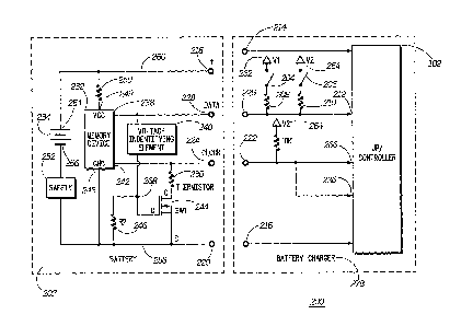
[00019] Referring to FIG. 2, a battery charging system 200 is illustrated. The
battery charging system 200 includes a battery charger 278 and a battery 202.
In a
preferred embodiment, the battery charger 278 is embedded within an electronic
device 100. Alternatively, the battery charger 278 is part of a stand-alone
device. For
example, a stand-alone charger can be a charger that receives power from a
power
supply and converts the power to a suitable level for charging a battery;
typically, a
stand-alone charger performs no other significant function. In contrast, the
electronic
device 100 is any component that cannot only charge a battery but also
performs other
important functions. Suitable examples of a host device include a computer, a
wireless telephone, or a radio. As the electronic device 100 in the preferred
embodiment is a phone, the host device will be hereafter referred to as a
"phone".
[00020] In one embodiment, the battery charger 278 detachably engages the
battery
202 for purposes of charging the battery 202 and/or powering the electronic
device
100. Specifically, the battery charger 278 includes a positive phone charging
contact
214, adapted to be coupled with a positive battery contact 218. The battery
charger
278 also includes a negative phone charging contact 216, adapted to be coupled
with a
negative battery contact 220. The phone 100 may be powered directly from the
positive battery contact 218 and the negative battery contact 220. In an
alternative
embodiment, the battery 202 includes a separate set of battery contacts (not
shown)
for providing power to the phone 100. As discussed in detail below, the
battery
charger 278 includes a battery charger data contact 226 for receiving a
battery data
contact 228, into which a data port 238 of a memory device 232 and a voltage
identifying element 240 terminates. The battery charger 278 includes a battery
charger clock contact 222 adapted for receiving a battery clock contact 224,
into
which a clock port 242 of the memory device 232 and a thermistor 230
terminates.
[00021 ] The battery 202 includes one or more cells 234, which discharge to
provide
power to the host device 100. The battery charger 278 recharges the cells 234
when
the cells 234 become depleted. Further, the cells 234 include a positive
terminal 254
6
CA 02556429 2006-08-15
WO 2005/081787 PCT/US2005/003649
coupled to the positive battery contact 218 for providing the positive voltage
B+ to the
host device through the positive battery node 260. In addition, the cells 234
includes a
negative terminal 256, coupled to a safety circuit 252 which prevents over-
charging or
under-charging the cells 234. In one embodiment, the safety circuit 252 may be
coupled to the negative battery contact 220, and in turn, provide a negative
voltage (B-
or ground point to the battery charger 278 through the negative battery node
258.
[00022] The battery charger 278 includes a microprocessor or microcontroller
102
and a pair of switches 204, 206, which will determine the function of the
battery
charger clock contact 222. The battery charger data contact 226 is coupled to
an
input/output (I/O) port 212 on the microprocessor 102, as well as coupled to
switch
204 and switch 206 through a pair of pull-up resistors 208, 210. Switch 204,
when
closed, pulls up the voltage on port 212 to the voltage level set by a first
voltage
source 262 having a voltage level noted as Vl (5.5V in a preferred
embodiment),
through resistor 208. Switch 206, when closed, pulls up the voltage on port
212 to the
voltage level set by a second voltage source 264, having a voltage level noted
as V2
(2.775V in a preferred embodiment), through resistor 210. Only one of switch
204
and switch 206 may be closed at any given time. The battery charger clock
contact
222 is coupled to the microprocessor 102 through an I/O port 266.
Additionally, the
battery charger clock contact 222 may also be coupled to the microprocessor
102
through an analog-to-digital (A/D) converter 236.
[00023] As noted earlier, the battery 202 includes a thermistor 230, a voltage
identifying element 240 and a memory device 232. The voltage identifying
element
240 and the thermistor 230 may be coupled by a switch 244. The switch 244 may
be a
transistor device, such as a FET, with the drain coupled to the thermistor
230, the
source coupled to the negative battery node 258, and the gate coupled to the
voltage
identifying element 240 and a resistor 21-6 at node 268.
[00024] The battery charger functions as follows. To read or write to the
memory
device 232, switch 206 would be closed and switch 204 opened, placing V2
(2.775V)
onto the battery charger data contact 226. The voltage identifying element 240
uses
the voltage at the battery data contact 228 ("data line") to set a control
voltage at node
7
CA 02556429 2006-08-15
WO 2005/081787 PCT/US2005/003649
268. The voltage identifying element 240 may include a zener diode, a resistor
divider network, a comparator, or any other voltage identifying device
commonly
known to those skilled in the art. When the voltage level is low enough or
high
enough not to enable switch 244, the thermistor 230 is switched off at the
battery
clock contact 224 ("clock line"). In this mode, the host device 100
communicates
with the memory device 232 via I/O ports 212 and 266 as normal.
[00025] Although the use of the clock line 224 in this embodiment is used to
read
the value of the thermistor 230. In another embodiment (not shown), the roles
of the
data and clock lines are reversed, where a voltage is placed on the data line
228 and
the value of the thermistor 230 is read from the data line as is understood by
those of
average skill in the arts.
[00026] To read the thermistor 230 value switch 204 would be closed and switch
206 would be opened, placing V 1 (5 . SV) onto the data line 228. The voltage
identifying element 240 then enables the voltage at node 268 high enough or
low
enough to allow switch 244 to conduct. In this mode, the thermistor 230 is
switched
onto the clock line 224, allowing the microprocessor 102.to the thermistor 230
value
via an analog-to-digital converter 236 as normally read. In this fashion, the
radio or
electronic device 100 selectively reads or writes to the memory device 232 or
read the
thermistor 230 without any interaction between the memory device 232 and the
thermistor 230. It is important to note that although switch 244 is shown as a
PNP
transistor, to those of average skill in the art, NPN transistors types could
be
substituted as well within the true scope and spirit of the invention.
[00027] In this arrangement, the power node 249 of the memory device 232 is
biased directly from the positive battery node 260 through resistor 250. The
ground
node 248 of the memory device is coupled directly to the negative battery node
248.
It will be obvious to those of ordinary skill in the art that this
configuration means that
the memory device 232 is continuously drawing current from the battery cells
234.
However, since the standby current of a typical EPROM or EEPROM is in the
single
digit microamp range, this current drain should be fairly insignificant.
8
CA 02556429 2006-08-15
WO 2005/081787 PCT/US2005/003649
[00028] In one arrangement, the battery charger 278 selectively reads the
memory
device 232 or a value of the thermistor 230. For example, this value can be
the
impedance of the thermistor 230, which the microprocessor 102 of the battery
charger
278 is used to monitor the temperature of the battery 202 as it is being
charged.
[00029] As another example, the memory device 232 is an EPROM that stores
information about the battery 202, such as the battery type, the charging
scheme to be
employed and the status of the charge of the battery 202. The microprocessor
102 of
the battery charger 278 reads the memory device 232 and uses this information
for
purposes of ensuring that the battery 202 is efficiently and properly charged.
[00030] Of course, it is understood that the memory device 232 is not limited
to
being an EPROM, as the memory device is any other suitable component capable
of
storing information, such as an EEPROM, non-volatile RAM, and FLASH memory.
Moreover, the memory device 232 is in no way limited to merely storing
information
about the status of the battery 202, as the memory device 232 stores any other
suitable
type of data. The actual functionality of the battery 202 is increased by
replacing the
EPROM on used in present battery designs with an EEPROM which increases the
overall functionality of the battery 202 by allowing battery information such
as, but
not limited to, charge cycles, date of last charge, power supply used, maximum
charge
current, maximum charge voltage, and temperature to be written to the EEPROM.
This information is used to help determine the root cause of return issues and
possible
safety issues, therefore reducing development and warranty costs. Furthermore,
by
allowing the single sourced custom EPROM used in most present designs to be
replaced by a lower cost, standard off-the-shelf EEPROM, the present invention
reduces the overall cost of the battery 202.
[00031 ] Additionally, by using the data line 228 to selectively switch in the
thermistor 230 on the clock line 224, the radio 100 is able to:
[00032] 1) read the battery temperature, and
[00033] 2) read/write the EEPROM without adding an additional contact to
achieve
this capacity.
9
CA 02556429 2006-08-15
WO 2005/081787 PCT/US2005/003649
[00034] This allows the standard four battery contact configuration to be
maintained.
[00035] While the preferred embodiments of the invention have been illustrated
and described, it will be clear that the invention is not so limited. Numerous
modifications, changes, variations, substitutions and equivalents will occur
to those
skilled in the art without departing from the spirit and scope of the present
invention
as defined by the appended claims.