Note: Descriptions are shown in the official language in which they were submitted.
CA 02557376 2006-08-28
METHOD OF SECURING AN ELECTRICAL SUB-CIRCUIT ASSEMBLY
TO A PRINTED CIRCUIT BOARD
FIELD OF INVENTION
[0001] This invention relates to securing electrical sub-circuit assemblies to
printed circuit boards.
BACKGROUND OF INVENTION
[0002] Within a main circuit system, there may frequently be a number of
individual sub-circuits which are each contained within a separate assembly,
which
may be a packaged assembly. Such sub-circuits may for example be transistor
dies,
integrated circuit dies or passive components. Both the physical attachment of
such
sub-circuit assemblies to a main circuit package and the electrical
interconnections
therebetween may be unreliable in terms of their rigidity and power handling
capabilities and often produce poor electrical impedance matching results
thereby
producing high insertion loss between the interconnections. Prior art methods
of
providing electrical conductivity between a main circuit and a sub-circuit
using bond
wires or bump connections often result in mismatch of the electrical circuits,
problems with high power capabilities, increased insertion loss and costly
manufacturing processes. Conventional bond wires can also cause parasitic
inductances, antenna effects and signal cross talk.
[0003] It is therefore an object of this invention to provide an improved
method of securing an electrical sub-circuit assembly to a printed circuit
board.
SUMMARY OF INVENTION
[0004] The present invention provides a method for coplanar attachment and
interconnection of electronic devices and assemblies by forming a cavity or
"basin"
feature within the main circuit platform. This basin accommodates the shape of
the
CA 02557376 2006-08-28
sub-circuit assembly, with the depth of the basin being equal to the thickness
of the
sub-circuit assembly, with suitable adjustment to accommodate any needed
adhesives
or solder necessary to fix the sub-circuit assembly to the main circuit
platform. The
basin can be formed for example by machining a finished laminate, such as by a
mechanical milling process or by laminating two or more suitably shaped planar
pieces together.
[0005] This invention provides a low cost and reliable circuit assembly
method by permitting a sub-circuit assembly to be placed directly on a main
circuit
platform by an automated machine, then physically fastened with proper
adhesive or
solder paste dispensed by an automated machine and then electrically connected
with
the aid of an automatic machine.
[0006] This invention renders it possible to both physically and electrically
attach either an individual component or a more sophisticated sub-circuit
assembly to
a main circuit platform such that one surface of the sub-circuit assembly is
coplanar
with the surface of the main circuit platform. Simple planar electrical
connection
techniques can then be applied between the sub-circuit and main circuit
assemblies,
thereby eliminating the need for bond wires and improving impedance match and
current carrying capabilities and reducing insertion loss between the sub-
circuit
assembly and the main circuit platform.
[0007] This invention also eliminates the need for a package to house the sub-
circuit assembly and the wire bonds or bump connectors which are used to
connect
within a package. The elimination of such a package permits the deposition of
biological or other chemical layers without the intrusion of wires or package
geometries.
[0008] This invention can be used in a wide range of electronic products.
Particular utility can be found in the following:
(a) Attachment of sensors: this invention is useful in attaching a sub-
circuit die to a platform assembly where the active surface of the die must
face
upwardly and be exposed. The active surface may include elements such as
biological and chemical sensors, MEMS devices and optical devices. These
sensors
would function in either the vapour or liquid phase. The active surface of the
die and
2
CA 02557376 2006-08-28
the platform assembly, being coplanar, will produce less aerodynamic or fluid-
dynamic turbulence or impediments in the vicinity of the active surface when
compared with conventional bond wire interconnections.
(b) Radio frequency (RF) products: the coplanar nature of interconnections
in accordance with the invention minimizes RF parasitic effects and impedance
mismatch, leading to higher operating efficiency and better performance. In a
cell
phone for example, this means better sensitivity and longer battery life. At a
more
detailed level, this interconnection technique in accordance with the
invention permits
direct microstrip launching from the main circuit board platform into a sub-
circuit
assembly which may house a RF semiconductor device. This invention enables the
removal of the high frequency barrier inherent to conventional bond wires at
microwave and millimetre-wave applications and the coplanar feature assists in
extending the operating frequency range.
This invention may also permit significant cost savings by eliminating
expensive coaxial or other interconnection methods between circuit boards.
Interconnection is particularly difficult with radio frequency circuitry. Over
a broader
range of electronic products, this invention provides an alternative to the
prevailing
motherboard/daughterboard paradigms in which daughterboards (sub-circuit
assemblies) are positioned either parallel or perpendicular to motherboards
(main
circuit assemblies) and interconnected by bulky and expensive connectors or
cables.
In radio frequency products, the ability to combine dissimilar platform
materials may lead to cost reduction. For example, a sub-circuit assembly
comprising
a small amount of higher cost low-loss material can be coplanar mounted into a
larger
cheaper yet higher-loss main circuit platform. The noise figure of a receiver
can be
enhanced by providing the sub-circuit LNA portion on a small low-loss material
such
as a ceramic material, while the main circuit can benefit from the low cost
and
mechanical strength of regular epoxy-fibreglass (FR4) circuit board material.
(c) Miniaturization and low profile design: this invention makes it possible
to make "flatter" circuit assemblies. By embedding the sub-circuit assemblies
within
the main circuit board, parts will not project above the main circuit board,
thus
3
CA 02557376 2006-08-28
resulting in potentially lower overall thickness of an assembly, and the
better
protection of components.
[0009] Typically, packaged sub-circuits which rely on bond wires to complete
electrical connections between the components and package are limited to the
size of
the bond wire and the inductance and resistive impedance characteristics of
the bond
wire. It is difficult to provide packaged sub-circuits which utilize
conductive bump
techniques with good inductance and resistance characteristics due to the
small cross-
sectional area at the point of electrical contact within the bump. The present
invention eliminates the costly package and electrical connectivity
requirement
between the component and package with bonding or conductive bump processes.
An
improvement in current carrying capabilities, less insertion loss and
impedance
matching may also be a direct result of the present invention. Instead of
having
electrical signals flow through very small diameter bond wires or the narrow
cross-
sectional area of conductive bumps, electrical signals with the present
invention can
flow through properly dimensioned electrical paths to maintain current
carrying,
insertion loss and impedance match integrity.
[0010] Interconnections which utilize small diameter bond wires typically
have a higher inductance and resistance values than for interconnections
utilizing
solder, conductive adhesive or SMT components. The inductance of a wire can be
approximated using equation 1 (from "RF Circuits Design", C. Bowick, Howard W.
Sams Company, ISBN: 0-672-21868-2).
Lwire = 0.002(1 2.3Log 4() - 0.75 (1)
D
[0011] For a wire of 0.001 inches in diameter (D) and 1 mm in length (1) a
value of 1.01 nH is derived from equation (1). This value compares favourably
with
3D bond wire electrical modeling data published by the Electrical Packaging
Group of
Amkor Technology. A value of 0.606 nH is derived from Amkor's 3D modeling
approximation found in equation (2).
L11 = 1.0703 (1) - 0.4641 (2)
4
CA 02557376 2006-08-28
[0012] The approximate inductance of a 0402 defined SMT resistance
component of zero ohms using equation (1) is 0.150 nH and is derived by
replacing
the width of the 0402 SMT with the diameter D of equation (1). This is a lower
value
than for a single bond wire of the same length. However, several bond wires in
parallel would reduce the bond wire inductance to a lower value than that of
the SMT
component's inductance but with much more additional complexity in the wire
bonding process.
[0013] The comparison of the resistance values of the bond wires versus the
SMT 0402 component is slightly more complicated as a phenomena called the skin
effect occurs. As the frequency of the signal passing through a conductive
block is
increased, the current tends to flow near the surface of the block and not
through its
centre. Equation (3) describes how the depth of this current carrying layer is
calculated.
s = 2 (3)
F
[0014] Where, w is the frequency component, is the permeability of the
current carrying block and a is the conductivity of the current carrying
block.
Typically, it can be assumed that the current flows in several layers each 8
thick for a
total of no thickness where n is the number of layers.
[0015] The calculation of the resistance for a wire of 0.001 inches in
diameter
(D) and 1 mm in length (1) is illustrated in equation (4), where area is the
cross-
sectional area of the bond wire where the current flows. This value is then
calculated
as 0.129 S2.
R = l (4)
6(Area)
[0016] This value again compares favourably with 3D bond wire electrical
modeling data published by the Electrical Packaging Group of Amkor Technology.
A
value of 0.127 f2 is derived from Amkor's 3D modeling approximation found in
equation (5).
CA 02557376 2006-08-28
R11 =128.7(l) - 2.0149 (5)
[0017] The approximate resistance of a 0402 defined SMT resistance
component of zero ohms using equation (4) and accounting for skin depth 6 is
0.000925 S2 and is again derived by replacing the width of the 0402 SMT with
the
diameter D for the calculation of the area of equation (4).
[0018] This large difference of resistance values between bond wires and the
SMT 0402 component would impact the current carrying capabilities of the bond
wire
along with an increase in losses when compared with the conductive adhesive
and
SMT 0402 component. Similar results would also apply to the narrow cross-
sectional
area associated with a conductive bump.
[0019] The present invention is specially useful with respect to sensor
devices
utilizing surface acoustic wave (SAW) or other acoustic wave (AW) devices.
[0020] Example of use of acoustic wave devices in conjunction with RF
components are well described in:
U.S. Patent No. 5,488,866, TIME-INTERLEAVED METHOD FOR
EFFICIENT OPERATION OF AN ACOUSTIC WAVE SENSOR ARRAY, and in
Hunt's publication, W.D. Hunt, D.D. Stubbs and S.H. Lee, "Time-dependent
Signatures of Acoustic Wave Biosensors," IEEE Proceedings, Vol. 91, no. 6, pp.
890-
901, June 2003.
[0021] The present invention is an improvement over Yatsuda's method
which incorporates conductive bumps but still requires a separate package,
described
in:
U.S. Patent No. 5,252,882, SURFACE ACOUSTIC WAVE DEVICE AND
ITS MANUFACTURING METHOD", and his publications;
H. Yatsuda, H. lijima, K. Yabe and 0. lijima "FLIP-CHIP STW FILTERS IN
THE RANGE OF 0.4 TO 5 GHZ," IEEE UFFC Symposium, October, 2002. Japan
Radio Co., Ltd., Kamifukuoka-shi, Saitama. 356-0011 Japan
6
CA 02557376 2006-08-28
Hiromi Yatsuda, Taira Horishima, Takeshi Eimura, and Takao Ooiwa
Miniaturized "SAW Filters Using a Flip-Chip Technique," IEEE TRANSACTIONS
ON ULTRASONICS, FERROELECTRICS, AND FREQUENCY CONTROL, VOL.
43, NO. 1, pp. 125-130, JANUARY 1996.
[0022] Another area in which this invention provides improvement is the
simpler refinement of the full-wave analysis using a finite-element simulation
between the package and bond wires. An example of this modeling is shown in:
C. Finch, Xiaomin Yang, T. X. Wu and B. Abbott, "RF Saw Filter Package
Design For Wireless Communications," Microwave And Optical Technology Letters,
Vol. 39, No. 5, December 5 2003.
[0023] The elimination of the bond wires will greatly reduce the complexity
of the connectivity model.
[0024] Other attempts to eliminate the wire bonds require soldering
techniques to complete the connectivity between the component die and the
electrical
substrate as shown in:
U.S. Patent No. 6,731,000 B1, Haque, FOLDED-FLEX BONDWIRE-LESS
MULTICHIP POWER PACKAGE.
Haque et al requires as described in this patent the placement of connectivity
studbumps on the die. These three dimensional studbumps allow for sufficient
contact
within a soldering process and may not function with a flat contact as
described
within this Patent. Coplanar design techniques would still be difficult with
Haque's
method.
[0025] The present invention is also well suited for sensor applications in
which a biologically coated acoustic wave device is submerged in water for the
detection of target molecules. The coplanar feature of die attachment provides
a
simpler method of placing a potting medium to cover the electrical portion of
the die
and not cover the biological area within the die. The submerged device would
only
7
CA 02557376 2006-08-28
allow an interface between the exposed biological layer and the water. Since
there are
no bonding wires protuding from the die which may be harmed during the potting
process, the coplanar method and structure of the present invention is a
significant
improvement over the prior art.
[0026] A coplanar bridge connection in accordance with the invention may
connect a transmission line microstrip structure onthe motherboard to a
corresponding
structure on the sub-circuit assembly (daughterboard). The bottom of the basin
can be
a groundplane which is contiguous between the sub-circuit assembly and the
motherboard. The benefit of such an interconnection is that it is receptive to
RF
signals, which is particularly important with ever-increasing computer central
processor operating frequencies and with the increasing miniaturization and
increasing operating frequencies of wireless devices.
[0027] Thus, this invention improves the method and structure of the sub-
circuit attachment process onto a main circuit electrical platform. The sub-
circuit
assembly being attached may be a discrete packaged or unpackaged die,
semiconductor device (transistor, diode, etc.), an integrated circuit in die
(or bumped
die) form, quartz devices such as crystals, filters, resonators, surface
acoustic wave
(SAW), surface transverse wave (STW), bulk acoustic wave (BAW), piezoelectric
transducers, micro mechanical systems (MEMS) devices, chemical sensors,
biological
sensors, light emitters and light sensors. A sub-circuit assembly is generally
attached
to an electrical platform which is a specially prepared printed circuit board
which
could be made from any common laminate material, including epoxy fibreglass,
phenolic, PTFE, alumina, etc. This invention is particularly effective for
attaching
sub-circuit assemblies which are incompatible with conventional soldering
techniques
used to attach components to circuit boards. Such incompatibility may be due
to
temperature sensitivity, or sensitivity to chemicals such as fluxes used in
the soldering
procedure within the electronics manufacturing process. This invention is also
particularly useful for attaching sub-circuit assemblies to main circuit
electrical
platforms in cases where the surface of the component used for electrical
connections
must be facing upwards and/or exposed to ambient environment.
8
CA 02557376 2006-08-28
DESCRIPTION OF THE DRAWINGS
[0028] Embodiments of the invention will now be described, by way of
example, with reference to the accompanying drawings, of which:
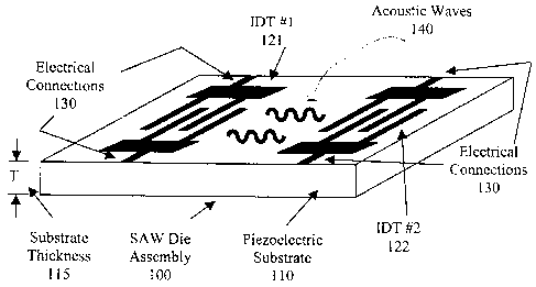
[0029] FIG.1 is a diagramatic perspective view of an acoustic wave device of
a bare die;
[0030] FIG.2 is a similar view of a main circuit platform comprising a multi-
layer printed circuit board in accordance with one embodiment of the
invention,
showing basin details and electrical pathways;
[0031] FIG.3 is a diagramatic plan view showing a SAW die placed in the
basin in the multi-layer printed circuit board;
[0032] FIG.4 is a similar view showing conductive adhesive dots placed on
both the die and electrical traces of the printed circuit board and a non-
conductive
adhesive to secure the die;
[0033] FIG.5 is a similar view showing zero Ohm SMT resistors located on
the conductive dots placed on both the dies and electrical traces of the
printed circuit
board;
[0034] FIG.6a is a diagrammatic perspective view of an acoustic wave device
on a bare die;
[0035] FIG.6b is a similar view showing a suitable coating for handling by an
SMT machine, and a window in the coating for exposing sensitive material; and
[0036] FIG.7 is a plan view of the product shown in FIG.6b with a conformal
coating layer over the main circuit platform for protection against vapours
and liquids.
DESCRIPTION OF PREFERRED EMBODIMENTS
9
CA 02557376 2006-08-28
[0037] Referring to the drawings a surface acoustic wave (SAW) die assembly
100 is shown in FIG. I. A first interdigital transducer (IDT) 121 is suitably
located on
a piezoelectric substrate 110 of thickness T 115. The IDT 121 transforms an
electrical signal into an acoustic wave and, being a reciprocal mechanism,
also
transforms an acoustic wave into an electrical signal. A second IDT 122 is
suitably
located along the propagation path of the acoustic waves 140. An IDT has
inherent
impedance which is a function of the physical geometry of the IDT. The IDT
electrical connections 130 can thus be designed to match the impedance value
of the
adjacent IDTs 121, 122. The electrical connections 130 are similar to
microstrip
geometries and are suitably scaled in dimensions to also achieve an impedance
equal
to the inherent impedance of the IDTs 120, 122. The electrical connections 130
are
located to bring the electrical interconnections of the circuit on the die
substrate 110
to the periphery thereof.
[0038] Other sub-circuit die assemblies with similar physical geometries are
also within the scope of this invention. The main criteria is that the
electrical
connections 130 bring to the physical periphery of the sub-circuit assembly
and the
die substrate 110 an electrical connection which matches the impedance of the
equivalent internal circuitry 121, 122. Sub-circuit die assemblies may also
have
electrical connections 130 positioned on either the top or bottom or both
layers of the
assembly.
[0039] Although the best benefit can be achieved if bare die sub-circuit
assemblies are attached to a main circuit electrical platform, it is also
within the scope
of the invention to attach packaged semiconductor devices to electrical
platforms,
such as circuit board assemblies with the actual packaged semiconductor
devices
being placed upsidedown. Packaged radio-frequency sub-circuits can be attached
to a
main circuit in this way with minimal impedance mismatch. The connectors of
the
packaged sub-circuit are equivalent to the electrical connections 130 shown in
FIG. 1.
[0040] The SAW die component shown in FIG.1 is placed within an electrical
platform 200 of the main circuit assembly shown in FIG.2. A multi-layer
printed
circuit board (PCB) is used as an example to explain the method and structure
of
coplanar die attachment. The first layer 211 with physical thickness T 205 has
electrical pathways 220 which provide electrical interconnections between
CA 02557376 2006-08-28
components of other electrical connections. Within the first layer 211, a
basin region
240 is located at the physical position where the sub-circuit assembly such as
the
piezoelectric die substrate 110 is to be located. The reservoirs 230 which
will receive
excess adhesive material are a result of cutting reliefs during the milling
process and
are suitably placed so as not to interfere with the electrical pathways 220.
In this
embodiment, the reservoirs 230 are placed at the four corners of the basin
region 240.
The basin region 240 exposes a second layer 212 of the electrical platform
structure
200 along with the electrical pathways 225 of the layer 212. The electrical
pathways
225 of layer 212 are physically expanded to allow the formation of a metal
ground
plane suitable for microstrip geometries. Other layers, up to layer n 213
complete the
structure of the electrical platform 200.
[0041] The basin region 240 can be formed either by machining a finished
laminate, by mechanical milling or other means of material removal, or by
laminating
two or more planar pieces together. For milling, the basin region 240 is
milled within
the first layer 211 to a depth equal to the thickness of a sub-circuit
assembly to be
attached with an adjustment to accommodate any needed adhesives and adjusted
in
thickness geometries to accommodate any needed adhesives or solder used to
affix the
sub-circuit assembly within the basin region 240. For lamination, two or more
layers
of laminate are joined together. The first layer 211 is the same thickness as
the sub-
circuit assembly with an adjustment to accommodate any needed adhesives or
solder
used to affix the sub-circuit assembly. The first layer 211 has a portion of
its material
removed before the lamination process to produce an opening which is the same
shape as the perimeter of the sub-circuit assembly. For a simple embodiment,
the
second layer 212 would be the bottom piece and be void of any basins, and the
first
layer 211 and the second layer 212 would be laminated together, forming the
basin
240.
[0042] The physical placement of a sub-circuit assembly such as a SAW die
assembly 302 within a basin region 340 located within an electrical platform
300 is
shown in FIG.3. The perimeter dimensions of the basin region 340 are such that
the
SAW die assembly 302 can be placed within the basin region 340 to minimize the
gap
between the SAW die assembly 302 and the top surface of the first layer 311.
The
dimensions of the basin region 340 are also such that electrical pathways 320
situated
11
CA 02557376 2006-08-28
on the surface of the first layer 311 align themselves with electrical
connections 322
of the SAW die assembly 302. The first surface layer 311 is coplanar with the
surface
of the SAW die assembly 302 such that both have a minimum difference in height
and
gap between them. For other assembly components, the dimensions and coplanar
positioning of a sub-circuit assembly would also be such that the electrical
pathways
320 and the second layer 212 shown in FIG.2 would align themselves with the
die
assembly electrical connections 322 located on either or both sides of the SAW
die
assembly 302. The reservoirs 330 are positioned so as not to interfere with
any
electrical pathways 320 or electrical connections 322. The reservoirs 330 are
constructed such that a part of the geometry of the die 302 either extends
into each
reservoir 330 or lies directly adjacent to it.
[0043] The physical attachment of a sub-circuit SAW die assembly 402 to a
main circuit electrical platform 400 is shown in FIG.4. Physical attachment of
the
SAW die assembly 402 to the main circuit electrical platform 400 is required
to
eliminate any possible lateral movement of the SAW die assembly 402 during the
electrical connection processing or post manufacturing of the main circuit
electrical
platform 400. The SAW die assembly 402 or other equivalent sub-circuit
assembly is
retrieved from a tray or reel and placed by a surface mount technology (SMT)
machine into a basin region 440. A non-conductive adhesive 435 is then
properly
dispensed either manually or with an automated process utilizing an SMT
machine,
stencilling, pin transfer or syringe-dispensing into the reservoirs 430. The
viscosity of
the non-conductive adhesive 435 is chosen so that it makes contact with the
SAW die
assembly 402, the geometric surfaces of the basin region 440 and the top
surface of
the second layer 212. For some non-conductive adhesive products, a temperature
curing process would then improve the rigidity of the non-conductive adhesive
435 to
prevent further movement of the SAW die 402. Curing the non-conductive
adhesive
can be achieved for example with ultraviolet light, moderate temperature
baking,
normal solvent evaporation or chemical reaction.
[0044] The electrical attachment of the SAW die assembly 402 to the main
circuit electrical platform 400 can be accomplished by several methods. A
first
12
CA 02557376 2006-08-28
method involves continuous conductive adhesive tracks 427 which are dispensed
either manually, or preferably with a placement/dispensing machine, beginning
on the
electrical pathways 420 of the electrical platform 400 and continuing with a
continuous conductive track onto the closely adjacent electrical connections
422. The
continuous nature of the conductive adhesive track 427 completes the
electrical
connection between the electrical pathways 420 and the adjacent electrical
connections 422.
[0045] A second method involves the placement of dots 425 of conductive
material on certain areas of the electrical pathways 420 and electrical
connections
422, the conductive material being in the form of conductive adhesive or
solder paste.
The conductive material can be dispensed either manually of with an automated
process utilizing a placement/dispensing machine, stencilling, pin transfer or
syringe
dispensing methods onto the electrical pathways 420 located on the electrical
platform
400 and separately onto the closely adjacent electrical connection 422 of the
SAW die
assembly 402. The resultant conductive dots 425 are positioned adjacent each
other at
the end extremities of the electrical pathways 420 and electrical connections
422.
[0046] This method is further illustrated in FIG.5. The completion of the
electrical circuits between the SAW die assembly 502 and other circuitry
located on
the electrical platform 500 and connected by electrical pathways 520 is
accomplished
by either a standard SMT zero ohm resistor or other value SMT component 528,
or
piece of conductive material, dispensed either manually or with an automated
process
onto the conductive dots 525. For example, both interconnection and AC
coupling
can be achieved simultaneously by using a chip capacitor SMT component 528.
Also,
active devices such as SMT packaged transistors or integrated circuits
including ball
grid arrays (BGAs) or flip-chips can be used instead of the SMT component 528.
For
some conductive material products, a temperature curing process can improve
both
the physical structure and the conductivity between the conductivity adhesive
material
525 and the SMT component 528. Curing can be achieved with ultraviolet light,
moderate temperature baking, normal solvent evaporation or chemical reaction.
In
the case of more robust devices which are temperature tolerant, the dots 525
of solder
paste conductive material can be processed by any common soldering method,
including convection reflow, vapour phase reflow, hot-plate conduction, hand-
13
CA 02557376 2011-05-06
soldering, wave-soldering and laser or xenon beam selective soldering. For
other sub-circuit
assemblies with similar physical geometries and with electrical connections
such as a ground
plane on the bottom face of a die, an initial step must be performed before
the die is placed
within the basin. The reservoirs, non-conductive adhesive and basin region are
denoted by
reference numerals 530, 535 and 540, respectively, in Figure 5. Referring to
FIG. 2, a
conductive material is suitably dispensed either manually or with an automated
process onto the
electrical pathways 225 of the second layer 212 before the die is place within
the basin.
[0047] An important issue which arises during placement of the sub-circuit
assembly on
the main circuit electrical platform is the potential damage to the exposed
circuitry on the surface
of the sub-circuit assembly during automated placement. By way of example,
FIG. 6a shows a
SAW die assembly 602 fashioned onto a piezoelectric substrate 610.
Interdigital transducers
such as first and second IDTs 621, 622 and electrical connections 630 are
typically fabricated
using thin film techniques. The thin film could be damaged as a vacuum chuck
or other handling
apparatus of an SMT machine imposes pressure on the die assembly 602. One way
of protecting
the die assembly 602 is to selectively coat part of the surface of the die
assembly with a
protective handling layer 660 as shown in FIG. 6b. The protective handling
layer 660 should be
applied as early as possible in the manufacturing process of the die and, if
possible, before the
die assembly is separated from its original wafer or equivalent form. The
protective handling
layer 660 can be arranged to provide correct exposure of the electrical
connections 630 and
thereby enable proper placement of the conductive adhesive 525, conductive
adhesive tracks 527
and the standard SMT components 528 shown in FIG. 5.
[0048] Such processing may also involve the provision of a window 670 in the
protective
handling layer 660. The window 670 permits the post processing of a suitable
sensitive material
680, such as a biological, polymer or other interface material, to be applied
to enhance the SAW
die assembly 602 in its role as a sensor. The sensitive material 680 is
attached to the exposed
surface of the die 602 and operates to transform measurable constituent vapour
or liquids which
can be detected by the circuit parameters of the sub-circuit assembly. The
window 670 exposes the
14
CA 02557376 2006-08-28
part of the die assembly circuitry, for example the first and second IDTs 621,
622
shown in FIG.6a and which produce the required sub-circuit assembly parameter
change.
[0049] Another important issue which then arises is the potential damage to
the circuitry and PCB when certain vapours or liquids come into contact with
areas
surrounding the window 670. FIG.7 illustrates how a conformal coating 700 can
cover the electrical platform 500, die assembly 502, electrical pathways 520,
electrical
connections 522, conductive adhesive dots 525, conductive adhesive tracks 527
and
the SMT components 528, as shown in FIG.5. This permits the sensitive material
780
and a partial protective handling layer area 760 to be exposed to a vapour or
liquid,
with the remainder of the circuit and components shown in FIG.5 being isolated
therefrom.
[0050] The advantages of the invention will now be readily apparent to a
person skilled in the art from the foregoing description of preferred
embodiments.
Other embodiments will also now be readily apparent, the scope of the
invention
being defined in the appended claims.