Note: Descriptions are shown in the official language in which they were submitted.
CA 02557472 2012-03-26
MICROMETRIC DIRECT-WRITE METHODS FOR PATTERNING
CONDUCTIVE MATERIAL AND APPLICATIONS TO FLAT PANEL
DISPLAY REPAIR
FIELD OF THE INVENTION
The invention generally relates to (i) a micron-scale, direct-write patterning
method using microfabricated (tipless) cantilevers coated with ink, which can
be called
Cantilever MicroDeposition; and (ii) its application to flat panel display
repair and
especially TFT LCD (thin film transistor liquid crystal displays) repair.
BACKGROUND
There is a strong commercial need in many current and emerging technology
fields for direct-write technologies capable of depositing materials, and
especially
metals and semiconductors, in patterns with features in the micron and sub-
micron size
regime. While most microelectronic devices are fabricated via
photolithography, the
need for direct write technologies is particularly evident in the area of
additive defect
repair and circuit edit. For instance, damaged or defective photomasks are
discarded at
extremely high costs to the microelectronics industry due to a lack of
suitable tools for
additive repair of missing material on nanoscale features. On the micron
length scale,
damage to the metal components of thin film transistor (TFT) arrays in flat
panel
displays (FPD) is difficult to repair due to the lack of rapid, low cost
methods for
depositing micron sized conductive traces. Although photolithography can be
carried
out for fabricating devices, it requires complex and costly instrumentation
which
makes the technology prohibitively expensive for low volume, high performance
components, or prototyping applications. In these cases, other techniques such
as
direct-write processes could offer unique advantages and
1
WO 2005/084092 CA 02557472 2006-08-24PCT/US2005/006009
capabilities. As the most common direct-write technology, ink-jet printing
offers a
convenient, flexible method for printing a range of different materials from
biological
molecules to materials for microelectronics. However, the resolution of the
technique
is generally limited to 15-200 micron-sized dots, which is not sufficient for
many
applications (see, for example, U.S. Patent Application 2004/0261700 to
Edwards et
al.). Other direct-write tools, such as laser-assisted deposition, electron or
ion beam
lithography, suffer either from similar resolution limitations, are too costly
for many
applications, or have material restrictions that will preclude their
application to the
direct fabrication or repair of active and passive microelectronic or
optoelectronic
components. In particular, electron-beam lithography, ion-beam micromachining,
laser- or electron-beam-assisted chemical vapor deposition requires a
(partial)
vacuum, which is prohibitively expensive for very large flat panels (such as
wide TV
or computer screens).
SUMMARY
The invention is further described with use of a non-limiting summary. A new
contact method for writing conductive metal features has been developed that
offers
controllable feature sizes from 100 micron to sub-micron dimensions. In this
method,
a (microfabricated) cantilever can be loaded with e.g. molecular or
nanoparticulate
ink which, by contacting a surface, is dispensed in very small quantities in
the form
of, for example, line and dot patterns. In the present form, both loading of
the
cantilever and deposition can be performed passively. However, by increasing
the
complexity of the microfabricated cantilevers, additional systems can
incorporate
active ink delivery. In addition, a number of metal precursor ink systems have
been
developed that are compatible with this method, so that patterning can be
carried out
with a large number of different metal and metal oxide materials. Importantly,
the
precursor inks can be patterned under ambient environmental conditions and
converted to metallic films at relatively low temperatures so that they can be
applied
to substrates such as, for example, plastics which cannot withstand high
temperature
processes.
In a preferred embodiment, the invention provides a method for writing, for
example, conductive metal or metal precursor comprising: providing a
cantilever
having a cantilever end, wherein the cantilever can be a tipless cantilever;
providing
an ink disposed at the cantilever end; providing a substrate surface; and
moving the
1155239.1 2
WO 2005/084092 CA 02557472 2006-08-24 PCT/US2005/006009
cantilever end or moving the substrate surface so that ink is delivered from
the
cantilever end to the substrate surface. The substrate surface can be moved
and the
cantilever held stationary, or the substrate surface can be moved and the
cantilever
held stationary. The movement which results in ink deliver can result
generally in
contact between the cantilever and the substrate surface, although their may
be
possibly be ink between the cantilever and the surface.
In another preferred embodiment, the invention provides a method for writing
conductive metal or metal precursor comprising: providing two or more
cantilevers
each having a cantilever ends, wherein the cantilevers can comprise a tip at
the end or
can be tipless cantilevers, wherein the cantilevers have a gap between them
which is
about one micron to about 20 microns; providing an ink disposed in the gap;
providing a substrate surface; contacting the two or more cantilevers with the
gap and
the substrate surface so that ink is delivered from the gap to the substrate
surface.
The invention also provides an ink formulation for microlithography or
nanolithography comprising: one or more metal salts and one or more solvents,
wherein the concentration of metal salt is about 1 mg/100 I, to about 500
mg/100
111,. The amount of the metal salt can be adjusted to be sufficiently high to
provide
suitable dispersion and suitable mass density and a thickness for a given
application.
The invention also provides a method for direct writing conductive metal
comprising: providing a cantilever having a cantilever end, wherein the
cantilever is a
tipless cantilever; providing an ink disposed at the cantilever end, wherein
the ink
comprises metallic nanoparticles; providing a substrate surface; contacting
the
cantilever end and the substrate surface so that ink is delivered from the
cantilever end
to the substrate surface.
Important advantages of the present invention include ability to operate in a
variety of different size regimes for a particular system including, for
example, the
about one micron to the about 15 micron regime or the about one micron to
about 10
micron regime (e.g., single digit) for lateral dimensions such as length and
width with
excellent control. Problems with clogging in nozzles or pipettes can be
avoided in
many embodiments. Instrumentation to do this is relatively straightforward and
does
not require, for example, high vacuum. Registration and versatility are
excellent.
Mass production and disposability are possible.
In addition, a series of numbered embodiments are also provided:
1155239.1 3
WO 2005/084092 CA 02557472 2006-08-24PCT/US2005/006009
1. A method of depositing a conductive coating in a desired pattern onto a
substrate comprising: depositing a precursor onto the substrate in the desired
pattern
by nanolithography with use of a tip coated with the precursor; contacting the
precursor with a ligand; applying sufficient energy to transfer electrons from
the
ligand to the precursor, thereby decomposing the precursor to form a
conductive
precipitate in the desired pattern and thus forming the conductive pattern
directly on
the substrate.
2. The method according to 1, wherein the tip is a nanoscopic tip.
3. The method according to 1, wherein the tip is a scanning probe microscopic
tip.
4. The method according to 1, wherein the tip is an atomic force microscope
tip.
5. The method of 1, wherein the coating comprises a metal with a purity of at
least about 80%.
6. The method of 1, wherein the coating comprises a metal with a thickness
of less than about 10 angstroms.
7. The method of 1, wherein the coating comprises a metal with a thickness
of at least about 100 angstroms.
8. The method of 1, wherein the precursor comprises a salt selected from the
group consisting of a carboxylate, a halide, a pseudohalide, and a nitrate.
9. The method of 1, wherein the precursor comprises a carboxylate.
10. The method of 1, wherein the pattern comprises a circuit.
11. The method of 1, wherein the ligand comprises a material selected from
the group consisting of an amine, an amide, a phosphine, a sulfide, and an
ester.
12. The method of 1 wherein the ligand is selected from the group consisting
of a nitrogen donor, a sulphur donor, and a phosphorous donor.
13. The method of 1 wherein the precipitate comprises a metal.
14. The method of 1 wherein the precipitate is selected from the group
consisting of copper, zinc, palladium, platinum, silver, gold, cadmium,
titanium,
cobalt, lead, tin, silicon and germanium.
15. The method of 1 wherein the precipitate comprises an electrical conductor.
16. The method of 1 wherein the precipitate comprises an electrical
semiconductor.
17. The method of 1 wherein the substrate comprises a non-conductor.
1155239.1 4
WO 2005/084092 CA 02557472 2006-08-24 PCT/US2005/006009
18. The method of 1 wherein the substrate comprises at least one of a
conductor and a semiconductor.
19. The method of 1 wherein the step of applying energy comprises applying
heat.
20. The method of 1 wherein the step of applying energy comprises applying
infra red radiation or UV radiation.
21. The method of 1 wherein the step of applying energy comprises applying
vibrational energy.
22. The method of 1 wherein the precursor comprises a salt selected from the
group consisting of a carboxylate, a halide, a pseudo halide, a nitrate, and
the ligand
comprises a material selected from the group consisting of an amine, an amide,
a
phosphine, a sulfide and an ester.
23. The method of 19, wherein the precipitate is selected from the group
consisting of copper, zinc, palladium, platinum, silver, gold, cadmium,
titanium,
cobalt, lead, tin, silicon and germanium.
24. The method of 19, wherein the step of applying energy comprises applying
radiant heat.
25. A method of printing a conductive metal in a desired pattern onto a
substrate comprising:
drawing a metal precursor and ligand directly onto the substrate according to
the desired pattern using nanolithography with use of a tip coated with a
precursor;
and
decomposing the precursor by applying energy to form the conductive metal
in the desired pattern, without removing from the substrate a substantial
quantity of
the precursor, and without removing from the substrate a substantial quantity
of the
metal.
26. The method of 25, wherein the metal pattern comprises a substantially
pure metal, with impurities less than about 20% by weight.
27. The method of 25, wherein the step of decomposing comprises thermally
decomposing.
28. The method of 25 wherein the step of decomposing comprises thermally
decomposing at a temperature of less than about 300 C.
29. The method of 25, wherein the metal is selected from the group consisting
1155239.1 5
WO 2005/084092 CA 02557472 2006-08-24 PCT/US2005/006009
of an elemental metal, an alloy, a metal/metal composite, a metal ceramic
composite,
and a metal polymer composite.
30. A nanolithographic method comprising:
depositing a metallic precursor from a tip onto a substrate to form a
nanostructure, and subsequently converting the precursor nanostructure to a
metallic
deposit.
31. The method according to 30, wherein the deposition and conversion is
carried out without use of an electrical bias between the tip and substrate.
32. The method according to 30, wherein the deposition and conversion is
carried out with use of a chemical agent other than the substrate.
33. The method according to 30, wherein the tip is a nanoscopic tip.
34. The method according to 30, wherein the tip is a scanning probe
microscopic tip.
35. The method according to 30, wherein the tip is an AFM tip.
36. The method according to 35, wherein the deposition and conversion is
carried out without use of an electrical bias between the tip and substrate.
37. The method according to 30, wherein the method is repeated to form a
multilayer.
38. The method according to 30, wherein the tip is adapted to not react with
the precursor.
39. The method according to 30, wherein the method is used to connect at
least one nanowire with another structure.
40. The method according to 30, wherein the method is used to connect at
least two electrodes.
41. The method according to 30, wherein the method is used to prepare a
sensor.
42. The method according to 30, wherein the method is used to fabricate a
lithographic template.
43. The method according to 30, wherein the method is used to prepare a
biosensor.
44. A nanolithographic method consisting essentially of:
depositing an ink composition consisting essentially of a metallic precursor
from a nanoscopic tip onto a substrate to form a nanostructure, and
subsequently
converting the metallic precursor of the nanostructure to a metallic form.
1155239.1 6
WO 2005/084092 CA 02557472 2006-08-24PCT/US2005/006009
45. The method according to 44, wherein the conversion is a thermal
conversion without use of a chemical agent.
46. The method according to 44, wherein the conversion is a chemical
conversion carried out with use of a reducing agent.
47. The method according to 44, wherein the reducing agent is used in the
vapor state to carry out the conversion.
48. The method according to 44, wherein the tip is an AFM tip.
49. The method according to 44, wherein the tip comprises a surface which
does not react with the precursor.
50. A method according to 44, wherein the method is repeated a plurality of
times to generate a multi-layer structure.
51. A method of printing without use of electrochemical bias or reaction
between the ink and substrate comprising depositing a metallic precursor ink
composition onto a substrate from a tip in the form of a microstructure or
nanostructure on the substrate to form an array having discreet objects
separated from
each other by about one micron or less.
52. The method according to 51, further comprising the step of forming metal
from the precursor.
53. The method according to 51, wherein the discreet objects are separated
from each other by about 500 nm or less.
54. The method according to 51, wherein the discreet objects are separated
from each other by about 100 nm or less.
55. A method for writing conductive metal comprising
providing a cantilever having a cantilever end, wherein the cantilever can
comprise a tip at the end or can be a tipless cantilever;
providing an ink disposed at the cantilever end;
providing a substrate surface;
contacting the cantilever end and the substrate surface so that ink is
delivered
from the cantilever end to the substrate surface.
56. The method according to 55, wherein the substrate surface is moved and
the cantilever is stationary.
57. The method according to 55, wherein the substrate surface is stationary
and the cantilever is moved.
58. The method according to 55, wherein the cantilever is a tipless
cantilever.
1155239.1 7
WO 2005/084092 CA 02557472 2006-08-24 PCT/US2005/006009
59. The method according to 55, wherein the cantilever comprises a tip at the
cantilever end.
60. The method according to 55, wherein the ink comprises one or more
metals.
61. The method according to 55, wherein the ink comprises one or more metal
salts.
62. The method according to 55, wherein the ink comprises one or more metal
nanoparticles.
63. The method according to 55, wherein the ink comprises one or more
hydrophobic nanoparticles.
64. The method according to 55, wherein the ink comprises one or more
hydrophilic nanoparticles.
65. The method according to 55, wherein the ink comprises one or more metal
nanoparticles having an organic shell.
66. The method according to 55, wherein the ink comprises one or more metal
nanoparticles having an insulating shell.
67. The method according to 55, wherein the ink is a hydrophobic ink.
68. The method according to 55, wherein the ink is a hydrophilic ink.
69. The method according to 55, wherein the ink is a hydrophobic ink, and the
substrate surface is a hydrophobic surface.
70. The method according to 55, wherein the ink is a hydrophilic ink, and the
substrate surface is a hydrophilic surface..
71. The method according to 55, wherein the ink comprises both hydrophobic
and hydrophilic agents.
72. The method according to 55, wherein the ink comprises one or more metal
nanoparticles having an average diameter of about 100 nm or less.
73. The method according to 55, wherein the ink comprises one or more
biological molecules.
74. The method according to 55, wherein the ink comprises one or more
peptides or proteins.
75. The method according to 55, wherein the ink comprises one or more
nucleic acids.
76. The method according to 55, wherein the ink comprises one or more sol-
gel materials.
1155239.1 8
WO 2005/084092 CA 02557472 2006-08-24PCT/US2005/006009
77. The method according to 55, wherein the ink comprises one or more
magnetic materials or precursors thereof
78. The method according to 55, wherein the ink comprises one or more
semiconductor materials or precursors thereof
79. The method according to 55, wherein the ink comprises one or more
optical materials or precursors thereof
80. The method according to 55, wherein the ink comprises one or more
solvents having a boiling point over 100 C.
81. The method according to 55, wherein the ink comprises one or more
compounds which chemisorb to or covalently bond with the substrate surface.
82. The method according to 55, wherein the ink forms a feature on the
substrate surface.
83. The method according to 55, wherein the ink forms metal oxide on the
surface.
84. The method according to 55, wherein the ink forms metal alloy on the
surface.
85. The method according to 55, wherein the ink forms a feature on the
substrate surface which has a dimension controlled by the geometry of the
cantilever.
86. The method according to 55, wherein the ink forms a feature on the
substrate surface which has a width of about one micron to about 100 microns.
87. The method according to 55, wherein the ink forms a feature on the
substrate surface and the feature is subjected to fusion, sintering, or
coalescence
conditions.
88. The method according to 55, wherein the ink forms a feature on the
substrate surface and the feature is subjected to annealing.
89. The method according to 55, wherein the ink forms a feature on the
substrate surface and the feature is subjected to light.
90. The method according to 55, wherein the ink forms a feature on the
substrate surface and the feature is subjected to laser.
91. The method according to 55, wherein the ink forms a feature on the
substrate surface and the feature is subjected to electrical current.
92. The method according to 55, wherein the ink forms a feature on the
substrate surface which contacts one or more electrodes on the substrate
surface.
1155239.1 9
WO 2005/084092 CA 02557472 2006-08-24PCT/US2005/006009
93. The method according to 55, wherein the ink forms a feature on the
substrate surface and is subjected to annealing at temperature of about 300 C
or less.
94. The method according to 55, wherein the ink forms a feature on the
substrate surface and is subjected to annealing at temperature of about 100 C
to about
300 C.
95. The method according to 55, wherein the ink is subjected to a reduction
reaction on the substrate surface.
96. The method according to 55, wherein the ink forms a feature on the
substrate surface which is made continuous after contacting.
97. The method according to 55, wherein the ink forms a feature on the
substrate surface which is converted to a metallic state which has a
resistivity of about
microohm*cm or less.
98. The method according to 55, wherein the ink forms a feature on the
substrate surface which is converted to a metallic state which has a
resistivity of about
1 microohm*cm to about 10 microohm*cm.
99. The method according to 55, wherein the ink forms a feature on the
substrate surface which has a width of about 5 nm to about one micron.
100. The method according to 55, wherein the method is repeated to form
layers of ink on the substrate surface.
101. The method according to 55, wherein the method is repeated to form
layers of ink on the substrate surface, wherein the inks are the same
material.
102. The method according to 55, wherein the method is repeated to form
layers of ink on the substrate surface, wherein the inks are different
material.
103. The method according to 55, wherein the ink forms a feature on the
substrate surface which is a line.
104. The method according to 55, wherein the ink forms a feature on the
substrate surface which is a dot.
105. The method according to 55, wherein the cantilever is an AFM
cantilever.
106. The method according to 55, wherein the substrate surface is glass.
107. The method according to 55, wherein the substrate surface is a thin film
transistor array.
108. The method according to 55, wherein the method is used to repair a flat
panel display.
1155239.1 10
WO 2005/084092 CA 02557472 2006-08-24PCT/US2005/006009
109. The method according to 55, wherein cantilever is loaded with ink with
use of a microfabricated inkwell filled with ink.
110. The method according to 55, wherein the cantilever is brought into
contact with the substrate surface at an angle of about 10 degrees or less.
111. The method according to 55, wherein the cantilever is brought into
contact with the substrate surface at an angle of about 5 degrees or less.
112. The method according to 55, wherein the cantilever is bent upon contact
as viewed by optical microscopy.
113. The method according to 55, wherein the contacting is carried out with
use of force-feedback.
114. The method according to 55, wherein the contacting is carried out with
use of piezoelectric scanning features.
115. The method according to 55, wherein the cantilever has a width of about
one micron to about 100 microns.
116. The method according to 55, wherein the cantilever has a width of about
five microns to about 25 microns.
117. The method according to 55, wherein the cantilever is a straight beam
shaped cantilever.
118. The method according to 55, wherein the contacting is carried out with
use of force-feedback.
119. The method according to 55, wherein the cantilever has a spring constant
of about 0.001 N/m to about 0.50 N/m.
120. The method according to 55, wherein the cantilever has a spring constant
of about 0.004 N/m to about 0.20 N/m.
121. The method according to 55, wherein the cantilever has a length of about
100 microns to about 400 microns.
122. The method according to 55, wherein the cantilever has a length of about
150 microns to about 300 microns.
123. The method according to 55, wherein the cantilever is one of a plurality
of cantilevers which deposit ink in parallel.
124. The method according to 55, wherein the ink is a polyol ink.
125. The method according to 55, wherein the ink comprises metal salts
together with one or more alcohols or polyols.
1155239.1 11
WO 2005/084092 CA 02557472 2006-08-24PCT/US2005/006009
126. The method according to 55, wherein the ink forms features on the
substrate surface having a lateral dimension of about one micron to about 15
microns.
127. The method according to 55, wherein the ink forms features on the
substrate surface which have a lateral dimension of about one micron to about
10
microns.
128. The method according to 55, wherein the ink forms features on the
substrate surface which have a lateral dimension of about one micron to about
15
microns.
129. A substrate comprising a substrate surface and an ink thereon prepared
by the method of claim 55.
130. A method for writing conductive metal comprising:
providing two or more cantilevers each having a cantilever ends, wherein the
cantilevers can comprise a tip at the end or can be tipless cantilevers,
wherein the
cantilevers have a gap between them which is about one micron to about 20
microns;
providing an ink disposed in the gap; providing a substrate surface;
contacting the two
or more cantilevers with the gap and the substrate surface so that ink is
delivered from
the gap to the substrate surface.
131. The method according to 130, wherein the gap is about one micron to
about five microns.
132. The method according to 130, wherein the gap is about five microns to
about ten microns.
133. The method according to 130, wherein the gap is about ten microns to
about twenty microns.
134. An ink formulation for nanolithography comprising: one or more metal
salts and one or more solvents, wherein the concentration of metal salt is
about 1
mg/100 1AL to about 500 mg/100 L.
135. An ink formulation according to 134, wherein the concentration of metal
salt is about 1 mg/100 L, to about 200 mg/100 1AL.
136. An ink formulation according to 134, wherein the concentration of metal
salt is about 5 mg/100 L to about 30 mg/100 L.
137. The ink formulation of 134, wherein the formulation further comprises
two or more oligomer or polymer additives having different average molecular
weight.
1155239.1 12
WO 2005/084092 CA 02557472 2006-08-24 PCT/US2005/006009
138. The ink formulation of 134, wherein the formulation further comprises at
least one oligomer and at least one polymer.
139. The ink formulation of 100, wherein the formulation comprises two or
more metal salts.
140. The ink formulation of 100, wherein the formulation further comprises
epoxy.141. A method for direct writing conductive metal comprising: providing
a
cantilever having a cantilever end, wherein the cantilever can comprise a tip
at the end
or can be a tipless cantilever; providing an ink disposed at the cantilever
end, wherein
the ink comprises metallic nanoparticles; providing a substrate surface;
contacting the
cantilever end and the substrate surface so that ink is delivered from the
cantilever end
to the substrate surface.
142. The method according to 141, wherein the ink forms a feature on the
substrate surface and the feature is subjected to post-treatment.
143. The method according to 141, wherein the ink forms a feature on the
substrate surface and the feature is subjected to heat treatment.
144. The method according to 141, wherein the ink forms a feature on the
substrate surface and the feature is subjected to light treatment.
145. The method according to 141, wherein the ink forms a feature on the
substrate surface and the feature is subjected to heat treatment below about
300 C.
BRIEF SUMMARY OF THE DRAWINGS
The patent or application file contains at least one drawing executed in
color.
Copies of this patent or patent application publication with color drawing(s)
will be
provided by the Office upon request and payment of the necessary fee.
Figure 1. Au Nanoparticles deposited between gold electrodes. (A) and (D)
optical
images of two lines approximately 60 and 45 [tm formed by drawing the inked
cantilever along the surface, the cantilever width were 60 and 45 lam
respectively. (B)
and (E) same patterns as in (A) and (D) after reduction. The measured
resistance
across the gap for these patterns is 32 and 18 Ohms. They resisted water
rinsing and
scotch tape test, as shown in (C) and (F), where the electrodes were pealed
off but not
the patterns.
1155239.1 13
WO 2005/084092 CA 02557472 2006-08-24PCT/US2005/006009
Figure 2. Au Nanoparticles deposited between gold electrodes. (A) and (B)
optical
images before and after curing of a line formed by drawing a 15 p.m inked
cantilever
between two electrodes. The measured resistance across the gap for this
pattern is 18
Ohms. The pattern resisted water rinsing and scotch tape test, as shown in
(C), where
the electrodes were pealed off but not the line pattern. (D) Topographic AFM
image
of 14.5 pm wide line and 90 nm height. (E) Corresponds to the cursor profile
of the
fabricated line.
Figure 3. Au Nanoparticles deposited between gold electrodes. (A) and (B)
optical
images before and after curing of a line formed by drawing a 15 pm inked
cantilever
between two electrodes. The measured resistance across the gap for this
pattern is 19
Ohms. (C) Topographic AFM image of 15.8 p.m wide line and 38 nm height, in the
red boxed area in (B). (D) Corresponds to cursor profile of the fabricated
line.
Figure 4. Au Nanoparticles deposited between gold electrodes. (A) and (D)
optical
images before and after curing of a line formed by drawing a 10 pm inked
cantilever
(narrowed using FIB, cantilever showed in the yellow box) across two
electrodes.
The measured resistance across the gap for this pattern is 9 Ohms. (B) and (E)
Topographic AFM images of 15.5 m wide line and 95 nm height and 11.5 m for
the FIB tip, in the red and blue boxed area in (D), respectively. (C) and (F)
correspond
to cursor profile of the fabricated line.
Figure 5. Au Nanoparticles deposited between gold electrodes. (A) and (B)
optical
images before and after curing of a line formed by drawing a 10 i.tm wide FIB
cantilever across two electrodes. The measured resistance across the gap for
this
pattern is 22 Ohms. (C)) Topographic AFM image of 11.5 pm wide line and 80 nm
height in the red boxed area in (B). (D) Corresponds to cursor profile of the
fabricated
line.
Figure 6. Au Nanoparticles deposited between gold electrodes. (A) and (D)
optical
images of a gold lines formed across two electrodes. The measured resistance
across
the gap for the line pattern in (A) is 190 Ohms. (B) and (E) Topographic AFM
images
of 5 and 4 p.m wide lines and 12 nm height, in the red and blue boxed area in
(A) and
(D), respectively. (C) and (F) correspond to cursor profile of the fabricated
line.
Figure 7. Au Nanoparticles deposited between gold electrodes. (A) and (D)
optical
images of a gold lines formed across two electrodes. (B) and (E) Topographic
AFM
images of 3 and 2 pm wide lines and 8 nm height, in the red and blue boxed
area in
1155239.1 14
WO 2005/084092 CA 02557472 2006-08-24PCT/US2005/006009
(A) and (D), respectively. (C) and (F) correspond to the cursor profile of the
fabricated line.
Figure 8. Platinum/gold alloy ink deposited between gold electrodes on silicon
oxide
using cantilevers. Each line was formed by dipping a cantilever into an ink-
filled
inkwell and then drawing a line until the cantilever ran out of ink. Note the
similarities in line shape and length.
Figure 9. Platinum/gold alloy ink deposited between gold electrodes on silicon
oxide
using adjacent cantilevers. Each of the three lines was fabricated using a
single
cantilever or adjacent cantilevers loaded with ink. The line on the left was
generated
by drawing a single 31 micron wide cantilever across the surface until it ran
out of ink
The widest, middle line was generated using 4 adjacent 31 micron wide
cantilevers,
and the right line was generated by 2 adjacent 31 micron wide cantilevers.
Note that
the maximum length of the lines increases with increasing number of writing
cantilevers.
Figure 10. AFM height images of nanoscale palladium patterns on silicon oxide.
Palladium acetate dissolved to saturation in 80% ethylene glycol was patterned
using
a PDMS coated silicon nitride AFM tip. The line scans of the cured patterns
reveal a
increase in height from 2 nm to 10 nm between the first and second layers.
Figure 11. AFM height images of nanoscale gold patterns on quartz. Gold
nanoparticle ink was patterned by holding an ink-coated conventional silicon
nitride
AFM cantilever/tip in contact with the surface for 10 s at a constant force.
The
rightmost row of dots (diameter 50 nm, height 3.5 nm) were formed at a force
of 0.2
nN, the middle row of dots were formed at a force of 1.5 nN (diameter 65 nm,
height
6 nm) and the leftmost row of dots were formed at a force of 4 nN (diameter 85
nm,
height 7.5 nm). The patterns were imaged immediately after patterning with the
coated tip.
Figure 12. AFM height images of nanoscale gold patterns on quartz. Gold
nanoparticles dissolved in mesitylene (the 'ink') were patterned by
translating an ink-
coated conventional silicon nitride AFM tip across the surface at a rate of
0.15
microns/s. The line trace indicates that the height and the width of the lines
increase
with applied force.
Figure 13. AFM height images of nanoscale gold patterns on quartz. Gold
nanoparticles dissolved in mesitylene (the 'ink') were patterned by holding an
ink-
coated conventional silicon nitride AFM tip in contact with the surface for 10
1155239.1 15
WO 2005/084092 CA 02557472 2006-08-24PCT/US2005/006009
seconds. The resulting pattern was cured for 10 seconds at 250 C using a heat
gun
and then imaged. After curing, the height of the particle patterns decreases
from
around 30 run to around 15 run.
Figure 14. Optical image of a micron scale platinum line drawn with a silicon
nitride
cantilever across gold electrodes on a silicon oxide wafer. The platinum ink
comprised platinum chloride dissolved in 80% ethylene glycol (100 mg in 15
microlitres). The precursor ink was converted to metal by heating on a hot
plate a
200 C for 20 s. The width of the line after curing was approximately 5
microns.
Figure 15. Optical image of a cured micron scale platinum line drawn with a
silicon
nitride cantilever across chromium electrodes on a glass wafer. The platinum
ink
comprised 100 mg of platinum chloride dissolved in 15 microliter aqueous
solution
containing 30 mg each of 300 and 10,000 molecular weight polyethylene glycol.
The
precursor ink was converted to metallic platinum by heating with a heat gun at
250 C
for 10 seconds.
Figure 16. AFM height image of nanoscale gold features drawn between gold
electrodes on silicon oxide. The gold precursor ink solution comprises 100 mg
of
gold tetrachloride salt dissolved in 80% ethylene glycol/20% water. The large
particles are a result of three layers of ink, with each layer cured by
heating on a hot
plate at 200 C for 10 seconds. This trace was not conductive.
Figure 17. Images of platinum-gold alloy patterns generated using AFM
cantilevers.
The alloy precursor ink comprised 100 mg of platinum salt and 50 mg of gold
salt co-
dissolved in 30 microliters of water containing 60 mg each of 300 and 10,000
MW
polyethylene glycol. The traces were cured by heating with a heat gun for 10
seconds
at 250 C. (A) A two layer pattern drawn across the 30 micron gap between gold
electrodes on a silicon oxide wafer. The resistance of the trace was 90 ohms.
(B) A
six layer pattern drawn between chromium electrodes on a glass wafer. The
resistance of the trace was 32 ohms. Figure 17(B) was carried out with use of
a
PDMS DPN stamp tip. (C) An AFM image showing the large grainy microstructure
of the platinum-gold alloy film; grain sizes were ¨150 nm.
Figure 18. An optical micrograph of a large gold feature on glass prepared
dropping
epoxy/gold precursor ink onto the slide and then curing for two hours at 150
C. The
gold precursor ink was prepared by dissolving 85 mg of hydrogen gold
tetrachloride
in 50 microliters of dimethylformamide and then adding 1 microliter of
ethylene
1155239.1 16
WO 2005/084092 CA 02557472 2006-08-24PCT/US2005/006009
glycol and 1 microliter of epoxy mixture to 3 microliters of this salt
solution. The
resistance of the film was 0.3 ohms.
Figure 19. An AFM height image of a gold pattern generated by depositing a
gold
precursor ink onto quartz using a PDMS-coated silicon nitride AFM tip. The
gold
precursor ink was prepared by dissolving 85.5 mg of gold tetrachloride (85.5
mg) in
50 1.1.1., of dimethylformamide. To this solution is added 1 1_, of ethylene
glycol and
0.1 mg of thiotic acid. The 4.5 x 4.5 micron square pattern was cured by
heating with
a hot air gun at 250 C for 10 seconds. The 1-layer pattern was 15 nm high
after
curing (see line trace).
Figure 20. Direct-writing of silver lines on a silicon nitride substrate using
a
commercial silver nanoparticle ink. (A) Optical image of the 200 um-long
silver ink
lines after direct writing; (B) Resulting silver microstructures after low-
temperature
curing; (C ) Topographic atomic force microscope image of a small portion of a
line
and corresponding average height profile, revealing that said line is 117.9 nm
thick.
Figure 21. Optical images showing cantilever microdepositions of a commercial
silver nanoparticle ink on a glass substrate before and after curing.
Figure 22. Deposition and low-temperature curing of a commercial silver
nanoparticle ink on a glass substrate coated with a chromium thin film. Laser
ablation
was used to form a gap in the chromium film and expose the underlying glass
substrate (in the center of the image). A tipless cantilever was then used to
draw two
lines onto the chromium film on each side of the laser-ablated gap and across
the gap.
Figure 23. Optical images illustrating the fabrication of multilayered lines
by
repeated drawing:
(1L) One-layer line with a 6 um width and 30 nm thickness;
(2L) Two-layer line with a 8.6 um witdh and 41 nm thickness;
(3L) Three-layer line with a 8 um width and 70 nm thickness.
Figure 24. Coating of a tipless cantilever with ink by dipping into a
microfabricated
reservoir. Top-view optical images of a cantilever (A) just above or (B)
dipping into a
pool of ink in a millimeter-wide circular reservoir (fabricated by deep
reactive ion
etching in a silicon wafer; bottom part of the image). Note the meniscus
around the
cantilever in image B.
Figure 25. Optical images illustrating the repair of a thin film transistor
(TFT) flat
panel display.
Figure 26. Schematic diagram of a tipless cantilever with an ink storage slit.
1155239.1 17
WO 2005/084092 CA 02557472 2006-08-24PCT/US2005/006009
Figure 27. Diagram illustrating four alternative designs for tipless slit
cantilevers.
Figure 28. Optical image illustrating the deposition of a commercial silver
ink on a
glass substrate with a slit cantilever.
Figure 29. Two examples of deposition and curing of lines made of silver
nanoparticle ink across a gap between gold electrodes on a glass substrate
when using
a slit cantilever.
Figure 30. Line writing with a slit cantilever loaded with a gold nanoparticle
/ 1,3,5-
TEB ink.
Figure 31. Diagram illustrating an instrument for the repair of flat panel
displays and
similar objects. It utilizes a cantilever or cantilevered microbrush coated
with a metal-
precursor ink to repair gaps in conductive traces. A XYZ stage controls the
cantilever's high-resolution motion. An inking mechanism comprising an inkwell
and
its protective cover supplies the material to the cantilever prior to the
touchdown
operation. A coarse Z- motion stage is provided for inking the cantilever and
contacting the surface, while a rotation stage can position it at any angle
about the Z
axis. Monitoring of the brightness of the cantilever (which varies with
bending) via
video imaging with the included camera system and appropriate image processing
software detects the touchdown of the cantilever on the surface when putting
it in
initial contact with the surface. A laser system is provided to (thermally)
cure the
microdeposited material.
Figure 32. Schematic diagram illustrating a second instrument for flat panel
repair. In
this design, the output of a laser reflective sensor is monitored as it
measures the Z
position of the cantilever, detecting touchdown of the cantilever on the
substrate
surface. As in the previous design, a few-nanometer-resolution XYZ stage
provides
cantilever motion, and a laser (not shown) cures the deposited material
("ink"). An
inking mechanism supplies the material ("ink") to the cantilever prior to the
touchdown operation. A large motion Z-stage moves supplies gross Z motion for
inking, while the rotation stage can position the cantilever at any angle
about the Z
axis.
Figure 33. Alternative design for a FPD repair instrument, in which a confocal
distance measurement device detects the touchdown of the cantilever on the
substrate
surface.
Figure 34. Optical images illustrating the deposition of conductive Au traces
deposited from a 5 p.m tipless cantilever loaded with gold nanoparticle ink
across
1155239.1 18
WO 2005/084092 CA 02557472 2006-08-24PCT/US2005/006009
insulating gaps of various widths (10, 20, 40 gm) between conductive ITO
(indium tin
oxide) electrodes.
Figure 35. Diagram illustrating how a gap may be formed near a topography step
when drawing a line using a tipless cantilever.
Figure 36. Diagram illustrating the loading and fabrication of micron-scale
(conductive) lines by direct-writing with a tipless cantilever coated with an
ink,
followed by curing. Experimental curing conditions are indicated that are
suitable for
low-temperature-curing inks, such as gold nanoparticle inks.
Figure 37. Diagram illustrating how the line width is controlled by (is
proportional
to) the cantilever width.
Figure 38. Experimental results illustrating how the line width is controlled
by (is
proportional to) the cantilever width. (A) A ten-micron-wide cantilever is
shown
writing a line of similar width. (B) A two-micron cantilever is shown writing
a circa
two-micron line. Both images are at the same scale for easier comparison of
the line
widths.
Figure 39. Optical and AFM images (A and B respectively) of conductive gold
traces
deposited across a 200 gm gap between chromium electrodes. A gold
nanoparticles /
mesitylene / decanol mixture (described in the additional working examples)
was used
in this experiment. The ink was converted to low-resistivity metallic form by
performing a high-temperature curing at 250 - 300 C for 7 minutes followed by
a
lower temperature curing at 120 C for 60 min.
Figure 40. Adhesion Tests. Single-layer gold lines were deposited onto glass
on three
adhesion test samples and cured for ¨10 seconds at 150 C. Tape peel tests
showed no
loss of adhesion to the substrate and the lines withstood chemical cleaning.
DETAILED DESCRIPTION
The invention, which can for convenience be referred to as "cantilever
microdeposition" (CMD) in its preferred embodiments, can be practiced in
numerous
embodiments, including those described below in the working examples.
1155239.1 19
WO 2005/084092 CA 02557472 2006-08-24PCT/US2005/006009
Embodiment 1: Cantilever Microdeposition
In a first embodiment, the invention provides a method for fabricating
micrometer-scale and submicrometer-scale patterns using a cantilever or
microbrush,
the method comprising (1) providing a cantilever or microbrush; (2) providing
an ink,
meaning a chemical compound or a mixture thereof, disposed on said cantilever
or
microbrush; (3) providing a substrate surface; and (4) contacting the
microbrush and
the substrate surface so that ink is delivered from the cantilever or
microbrush to the
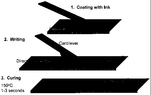
substrate surface. Figure 36 illustrates the principle of this method.
Preferably, the smallest lateral dimension of the resulting pattern (measured
parallel to the substrate surface, e.g. the width of a line) ranges from 0.5
micron to 15
microns. Its largest lateral dimension (e.g. the length of a line) exceeds 100
microns
and preferably 200 microns, and its height (e.g. measured substantially
orthogonally
to said local plane) ranges from 1 nm to 2 microns.
Preferably, the cantilever or microbrush is a microfabricated device, meaning
a microelectromechanical system (MEMS) fabricated using standard
microfabrication
techniques, including but not limited to photolithography, electron beam
lithography,
thin film deposition, etching, lift-off and focused ion beam micromachining.
The
microbrush may have the shape of a cantilever having a free end and an end
bound to
a macro- or mesoscopic body or it may be a device comprising a multiplicity of
cantilevers. The cantilever(s) may be with or without tip(s) protruding out of
the
principal plane of the cantilever. The meso/macroscopic body may be a diced
(silicon
or glass) wafer.
Two or more neighboring cantilevered bodies may form a gap or slit of fixed
or variable width that may be used for ink storage or dispensing. A
microfluidic
circuit may be formed on/in the cantilevered bodies and/or the meso- or
macroscopic
body it is attached to. The microfluidic circuit may comprise reservoirs,
channels, and
vias for ink delivery. Channels and reservoirs may be formed by two
substantially
parallel surfaces (such as the walls of the slits described above) or by three
or more
surfaces (e.g. forming an open channel or a completely enclosed channel). In a
preferred embodiment, a substantially flat, tipless cantilever is used.
Many inks may be deposited, including organic and inorganic compounds,
including metal salts and complexes, sol-gel precursors, polymers,
biomolecules such
1155239.1 20
CA 02557472 2012-03-26
as nucleic acid (e.g. DNA), peptides and proteins, nanoparticles and solutions
or
mixtures thereof. Deposition may be preceded or followed by a number of
treatments,
including substrate cleaning, surface preparation, hole drilling,
micromachining with a
laser or ion beam, photolithography and curing by application of heat or
light.
Literature useful for practicing the invention
Cantilevers, tips, inks, substrate surfaces, and contact methods are known in
the
art, and one skilled in the art can refer to the following technical
literature in the
practice of the present invention in its many embodiments including the
preferred
embodiments and working examples described below.
Cantilever microdeposition is related to but distinct from Dip Pen
NanolithographyTM (DPNTM) printing, a technology commercially developed by
NanoInk, Inc. (Chicago, IL), in which typically (1) a sharp tip with a
nanometer-scale
apex is coated with an ink; (2) the ink flows from the tip onto a substrate
through a
meniscus that naturally condenses at the contact junction. In contrast to DPN
printing,
the present invention does not require a sharp tip but rather preferably uses
a flat,
spatula-like micrometer-sized cantilever or cantilever as the ink application
means.
Cantilever microdeposition is best used for the fabrication of patterns with a
critical
dimension from the high submicrometer to ten-micron range, while DPN printing
is
best for very-high-resolution (e.g. nanoscale) patterning.
While its resolution is lower, the throughput of cantilever microdeposition
(in
square microns per second) is higher than that of DPN printing, especially
since higher
speed (of the cantilever or microbrush relative to the surface) may be used.
Generally speaking, the cantilever used in the present invention does not
contact
directly the surface of the substrate. Rather, a layer of ink is trapped
between the
surface and the microbrush or cantilever end. Without wishing to be bound by
theory,
it is believed that the interplay of hydrodynamics and capillary tension in
the space
between the cantilever and the surface controls ink deposition. For example,
the
pattern height and overall quality (continuity) is sensitive to the pressure
applied to the
cantilever, while in DPN this is generally not the case. The line width is
highly
21
= CA 02557472 2012-03-26
correlated to the cantilever width (see Figures 37 and 38, for example) and
mostly
independent from the patterning speed, while in contrast, with DPN printing,
it is
controlled by the diffusion rate of the ink from a point source (the tip-
sample contact)
and the patterning speed.
However, a lot of the technical developments associated with Dip Pen
Nanolithography, including but limited to inks, ink delivery technology,
cantilever/
brush fabrication processes, cantilever position control technology and
computer-
control design and fabrication algorithms, are highly relevant to cantilever
microdeposition.
A variety of products related to DPN printing can be obtained from NanoInk
including deposition instruments (e.g. the NSCRIPTORTm platform), computer
software,
environmental chambers, pens, substrates, kits, inks, inkwells, calibration
software,
alignment software, accessories, and the like. Single DPN printing probes,
passive
multi-probe arrays, A-frame cantilevers, diving-board-shaped cantilevers, as
well as
AC-mode cantilevers can be obtained from NanoInk. Also available are sharpened
and unsharpened tips. DIP PEN NANOLITHOGRAPHYTm and DPNTM are
trademarks for NanoInk, Inc., Chicago, IL) and are used accordingly herein.
DPN printing and deposition methods are extensively described in the
following patent applications and patent publications, particularly with
respect to the
experimental parameters for carrying out the deposition:
1. U.S. Provisional application 60/115,133 filed January 7, 1999 ("Dip Pen
Nanolithography") now U.S. Patent No. 6,635,311 to Mirkin et al. issued
October 21,
2003.
2. US. Provisional application 60/157,633 filed October 4, 1999 ("Methods
Utilizing Scanning Probe Microscope Tips and Products Therefor or Produced
Thereby") now U.S. Patent No. 6,635,311 to Mirkin et al. issued October 21,
2003.
3. U.S. Regular patent application 09/477,997 filed January 5, 2000 ("Methods
Utilizing Scanning Probe Microscope Tips and Products Therefor or Produced
Thereby"), now U.S. Patent No. 6,635,311 to Mirkin et al. issued October 21,
2003.
4. U.S. Provisional application 60/207,713 filed May 26, 2000 ("Methods
Utilizing Scanning Probe Microscope Tips and Products Therefor or Produced
Thereby"), now U.S. Patent No. 6,827,979. This application, for example,
describes
wet chemical etching, working
22
= CA 02557472 2012-03-26
examples, references, and figures.
5. U.S. Provisional application 60/207,711 filed May 26, 2000 ("Methods
Utilizing Scanning Probe Microscope Tips and Products Therefor or Produced
Thereby"), now U.S. Patent No. 6,827,979.
6. U.S. Regular application 09/866,533 filed May 24, 2001 ("Methods Utilizing
Scanning Probe Microscope Tips and Products Therefor or Produced Thereby"),
now
U.S. Patent No. 6,827,979. This application, for example, describes wet
chemical
etching, working examples (e.g., example 5), references, and figures.
7. U.S. patent publication number 2002/0063212 Al published May 30, 2002
("Methods Utilizing Scanning Probe Microscope Tips and Products Therefor or
Produced Thereby").
8. U.S. patent publication number 2002/0122873 Al published September 5,
2002 ("Nanolithography Methods and Products Produced Therefor and Produced
Thereby").
9. PCT publication number WO 00/41213 Al published July 13, 2000 based on
PCT application no. PCT/US00/00319 filed January 7, 2000 ("Methods Utilizing
Scanning Probe Microscope Tips and Products Therefor or Produced Thereby").
10. PCT publication number WO 01/91855 Al published December 6, 2001
based on PCT application no. PCT/US01/17067 filed May 25, 2001 ("Methods
Utilizing Scanning Probe Microscope Tips and Products Therefor or Produced
Thereby").
11. U.S. Provisional application 60/326,767 filed October 2, 2001, ("Protein
Arrays with Nanoscopic Features Generated by Dip-Pen Nanolithography"), now
published 2003/0068446 on April 10, 2003 to Mirkin et at.
12. U.S. Provisional application 60/337,598 filed November 30, 2001,
("Patterning of Nucleic Acids by Dip-Pen Nanolithography"), now U.S. Patent
No.
7,361,310 and U.S. regular application 10/307,515 filed December 2,2002 to
Mirkin
et at., now U.S. Patent No. 7,361,310.
13. U.S. Provisional application 60/341,614 filed December 17, 2001,
("Patterning of Solid State Features by Dip-Pen Nanolithography"), now
published
2003/0162004 August 28, 2003 to Mirkin et al. This application includes
descriptions
of metallic, metal oxide, and inorganic solid state structures.
23
= CA 02557472 2012-03-26
14. U.S. Provisional application 60/367,514 filed March 27, 2002, ("Method
and Apparatus for Aligning Patterns on a Substrate"), now publication no.
2003/0185967 on October 2, 2003 to Eby et al.
15. U.S. Provisional application 60/379,755 filed May 14, 2002,
("Nanolithographic Calibration Methods"), now Patent No. 7,060,977 and U.S.
regular
application 10/375,060 filed February 28, 2003 to Cruchon-Dupeyrat et al., now
Patent
No. 7,060,977.
16. In addition, US regular application 10/647,430 (now published,
2004/0127025) filed August 26, 2003 to Crocker et al. ("Processes for
fabricating
conductive patterns using nanolithography as a patterning tool") describes a
variety of
metal inks which can be patterned according to the present invention (much of
the text
is provided below to further enable one skilled in the art to practice the
present
invention). Also, US regular application published as 2004/0026681
("Protosubstrates") to Cruchon-Dupeyrat et al. published February 12, 2004
describes
a variety of embodiments for printing micro and nano structures which can be
tested
on a macro scale. Also, US regular application published January 15, 2004 to
Mirkin
et at. ("Electrostatically Driven Nanolithography") publication no.
2004/0008330
describes patterning of conductive polymers. Also, US regular application
10/442,189
filed May 21, 2003 to Mirkin et al. ("Peptide and Protein Nanoarrays and
Direct-Write
Nanolithographic Printing of Peptides and Proteins"), now Patent No.
7,716,036,
describes a variety of peptides and proteins which can be patterned according
to the
present invention. Also, U.S. patent application serial no. 10/689,547 filed
October
21, 2003 to Van Crocker etal. ("Nanometer Scale Engineering Structures..."),
now
Patent No. 7,691,541. Also, U.S. patent application 10/705,776 filed November
12,
2003 to Cruchon-Dupeyrat et al. ("Methods and Apparatus for Ink Delivery..."),
now
Patent No. 7,034,854.
In general, state of the art DPNTM printing and deposition-related products,
including hardware, software, and instrumentation are also available from
NanoInk,
Inc. (Chicago, IL), and these can be used to carry out the present invention.
For
example, NSCRIPTORTm instrumentation can be used for patterning. DPN printing
is
further described in, for example, Ginger, Zhang, and Mirkin, Angew. Chem.
Int. Ed.,
2004, 43(1), 30-45.
24
CA 02557472 2012-03-26
Parallel methods of the DPN printing process can be carried out as described
in, for example, U.S. Pat. No. 6,642,129 to Liu et al. issued November 4,
2003.
In addition, the following papers describes wet chemical etching procedures
used in conjunction with direct-write nanolithography: Zhang et al., "Dip-Pen
Nanolithography-Based Methodology for Preparing Arrays of Nanostructures
Functionalized with Oligonucleotides"; Adv. Mat., 2002, 14, No. 20, October
16, pages
1472-1474; Zhang et al., "Biofunctionalized Nanoarrays of Inorganic Structures
Prepared by Dip-Pen Nanolithography"; Nanotechnology, 2003, 14, 1113-1117;
Zhang
etal., "Fabrication of Sub-50 nm Solid-State Nanostrcutures on the Basis of
Dip-Pen
Nanolithography"; Nano Lett., 2003, 3, 43-45. In addition, U.S. patent
application
"Fabrication of Solid-State Nanostructures including sub-50 nm Solid-State
Nanostructures Based on Nanolithography and Wet Chemical Etching" (serial no.
10/725,939 filed December 3, 2003 to Mirkin et al.), now Patent No. 7,291,284,
also
describes etching and monolayer resists which can be used in the invention.
The text Fundamentals of Microfabrication, The Science of Minitaturization,
2nd Ed., Marc J. Madou, describes micro and nanotechnologies including
additive and
substractive methods, for example, lithography (Chapter 1), pattern transfer
with dry
etching methods (Chapter 2), pattern transfer with additive methods (Chapter
3), and
wet bulk micromachining (Chapter 4). Also, the text Direct-Write Technologies
for
Rapid Prototyping Applications: Sensors, Electronics, and Integrated Power
Sources
(Eds. A. Pique and D.B. Chrisey), describes micro and nanotechnologies
including
additive and substractive methods. For example, bulk micromachining and
etching are
described on pages 617-619. DPN printing on the Sub-100 nanometer length scale
is
described in Chapter 10.
Additional Embodiments
Embodiment 2: Cantilever microdeposition and curing for producing
conductive metallic and other patterns
In a preferred embodiment, for example, the invention provides a method for
writing conductive metal comprising: (1) providing a cantilever having a
cantilever
end, wherein the cantilever can comprise a tip at the end or can be a tipless
cantilever;
25
= CA 02557472 2012-03-26
(2) providing an inkdisposed at the cantilever end; (3) providing a substrate
surface;
and (4) contacting the cantilever end and the substrate surface so that ink is
delivered
from the cantilever end to the substrate surface. The deposition is preferably
followed
by localized heat curing step e.g. by use of a medium-power laser or an
infrared gun.
In another preferred embodiment, stamp tips are used to deposit material which
are described further below. Stamp tips are described in, for example, U.S.
provisional
patent application 60/544,260 entitled "Direct-Write Nanolithography with
Stamp Tip:
Fabrication and Applications" to H. Zhang et al. and filed February 13, 2004,
now
Patent No. 7,491,422, and US regular patent application serial no. 11/056,391
filed
February 14, 2005, now Patent No. 7,491,422.
Cantilevers are known in the art and are available from, for example,
MikroMasch USA (Portland, OR). Cantilevers can be coated and functionalized as
desired. Tipless cantilevers are also known in the art as described in, for
example,
U.S. Patent Nos. 5,958,701 to Green et al.; 6,524,435 to Agarwal etal.; and
6,573,369
to Henderson et al.
An important feature of the invention is that the geometry and shape of the
cantilever can be used to control at least one dimension of the features
formed on the
substrate surfaces from inks.
The ink is not particularly limited, although a primary embodiment of the
invention is metal-based inks, including both metal precursor inks, often
using metal
salts, and metal nanoparticulates inks. Useful embodiments are described
further in
patent application no. 16 (conductive patterns) noted above and described
further
below.
In general, the three primary ink components include (1) the primary material
to be deposited such as, for example, one or more metals or metal salts, (2)
one or
more solvents, and (3) one or more additives if desired. One can adjust the
components of the ink to function together with the cantilever, the tip if
present, and
the substrate.
Inks can be fully or partially dried, if desired, on the cantilever or the
cantilever
tip before delivery to the substrate surface. Inks can be fully or partially
dried on the
substrate surface after delivery.
The nanoparticles of the ink are not particularly limited although a primary
embodiment of the invention is metal-based inks. Inorganic compounds can be
used
26
WO 2005/084092 CA 02557472 2006-08-24PCT/US2005/006009
in the nanoparticles. The nanoparticles can be substantially homogeneous or
can be
heterogeneous. They can have a core-shell structure if desired. They can have
organic surface coatings or shells if desired. They can be magnetic in nature.
They
can be semiconductive in nature, whether doped or undoped. Nanoparticles can
be
electrically insulating or have an insulating shell. The nanoparticles can be
hydrophilic or hydrophobic. Nanoparticles can also be precursors to other
technologically useful materials including electrical conductors, magnetic
materials
including ferromagnetic materials, semiconductors, and optical materials.
Nanoparticles can exhibit quantum confinement effects and show useful
properties
such as for example electroluminescent and photoluminescence of various
colors.
Nanoparticles can be ftinctionalized to chemisorb to or covalently bond to the
surface.
The solvent system is not particularly limited. Ink solvents which are high-
boiling are generally preferred. For example, solvents with boiling points
above
about 100 C and more particularly above about 150 C can be used. Aromatic
hydrocarbons are one kind of high boiling solvent for example.
Upon delivery to the substrate surface, the inks can begin drying as desired
for
form features which are preferably stable over time after, for example, one
month.
Preferably, the features can be cured and made stable against rinsing with
solvents
including aggressive solvents and etching systems. Features can be subjected
to
annealing, light, lasers, electric currents, and other stimulations.
Often, it is desired to form continuous masses of structures which provide,
for
example, high electrical conductivity. Often it is desired to form high
quality contacts
between the features and the surface or other features on the surface such as,
for
example, electrodes.
Features can be nanostructures or microstructures. The height of the feature
is
not particularly limited as layering can be carried out to build up height.
Lateral
dimensions such as length and width are not particularly limited as the
methods
described herein can be used to prepare nanoscale and micron scale dimensions.
For
example, dot diameter or line width can be, for example, about 5 nm to about
one
micron. Alternatively, dot diameter or line width can be, for example, about
one
micron to about 100 microns, or about 5 microns to about 25 microns.
Additional references are described throughout the rest of the specification
for
use in practicing the present invention. No admission is made that any of
these
1155239.1 27
WO 2005/084092 CA 02557472 2006-08-24PCT/US2005/006009
references are prior art. The invention is further described by the following
non-
limiting examples.
WORKING EXAMPLES
In the following examples, gold and platinum traces were written by this new
method to yield low resistivity traces that adhere strongly to substrates such
as glass.
The working examples are subdivided into (1) an experimental section, and (2)
results
and discussion.
Experimental
Materials
All metal salts were purchased in highest available purity from Aldrich
(Milwaukee, WI). Silicon nitride cantilevers with tips and without tips and
with
different beam widths were prepared via standard microfabrication methods. To
further test the effect of cantilever width, some cantilevers were narrowed
using
focused ion beam (FIB) technology.
Nanoparticle preparation
Nanoparticles were prepared using the method described by Murray and
coworkers in M. J. Hostetler, et al., Langmuir 14, 17 (1998).
Patterning
Micron sized patterns were generated using the translation stages of
Thermomicroscopes CP Research instruments or NSCRIPTOR (NanoInk, Chicago, IL)
instruments. Cantilevers were coated with different metal precursor inks by
using the
z-stepper motors to bring the cantilevers into contact with microfabricated
inkwells
filled with ink. The z-motor and x-y translation stage were then used to
position the
coated cantilevers over the substrate, and to bring the cantilever into
contact with the
surface. The cantilevers were brought into contact at a slight angle (several
degrees)
so that only the end of the cantilever touched the surface. A slight bending
of the
flexible cantilever as monitored by optical microscopy indicated that contact
has been
achieved. Note that for patterning micron scale features, it was not necessary
to use
the force feedback and piezoelectric scanning/positioning features of the
instruments.
However, for nanoscale patterns these fine positioning features provided
control of
feature size and alignment at the sub-micron and in some cases sub-100 nm
scale.
1155239.1 28
WO 2005/084092 CA 02557472 2006-08-24PCT/US2005/006009
Results and Discussion
Ink Deposition.
A new method for directly writing ink on surfaces was developed that enables
line and dot patterns with dimensions of hundreds of microns and as small as
sub-
micron. The ink delivery method involved the following general steps:
Ink Loading. A flexible cantilever was loaded with an ink. Depending on the
application, the cantilever can have a sharp tip on the end, or be tipless,
and can have
various end shapes and widths, from several microns to hundreds of microns.
Ink
loading can be performed passively by bringing the cantilever in contact with
a
droplet or reservoir of ink and then removing it. The ink wets the underside
of the
cantilever and adheres through cohesive forces. Passive loading and delivery
of ink
was demonstrated in the working examples. The methods described by C. Bergaud
and collaborators to actively draw up liquid inks and control the deposition
via
electrowetting and dielectrophoresis can be also used.
Approach. The cantilever can be brought into contact with the surface for
patterning.
In most cases, a laser force-feedback mechanism is not required, nor is a
piezoelectric
scanning/positioning mechanism required. Mechanical "Z" stepper motors can be
used to bring the cantilever into contact with the surface, and optical
microscopy can
be used to detect defection of the cantilever when it comes into contact with
the
surface.
Feature Control. Line patterns can be formed by drawing the cantilever along
the
surface. With NSCRIPTOR and Thermomicroscope CP Research platforms "X" and
"Y" stepper motors or fine manual positioning screws can be used to translate
the
lever along the surface in the form of the desired pattern. Commercial high-
resolution
piezoelectric stage (NPoint, Madison, WI) may be retrofitted in either
instrument.
With the NSCRIPTOR platform, one can use custom pattern design software to
direct
the motion of the cantilever.. Importantly, if the cantilever is translated
along the
surface in the direction of the long axis of the cantilever, the width of the
line can be
directly related to the width of the end of the cantilever as shown in Figure
1. Thus,
one can control the shape of the lines, e.g. the width of the lines, via the
geometry of
the cantilever. Using standard microfabrication techniques it is possible to
fabricate
cantilevers with widths of about 1 micron to about 100 microns. Therefore,
with this
method, line patterns can be generated that have widths under a micron to well
over
1155239.1 29
WO 2005/084092 CA 02557472 2006-08-24PCT/US2005/006009
100 microns. The large range of line widths that can be patterned using
various
cantilever configurations is shown in Figures 1 through 7. For example, Figure
1
shows optical images of 60 and 45 micron wide lines. Figure 6 shows optical
and
AFM height images of 5 and 4 micron wide lines, and Figure 7 shows 3 and 2
micron
wide lines. Even at the narrowest line widths, the lines are sufficiently
continuous to
yield resistivities as low as 4 microohm.cm.
The best feature control was achieved with straight beam shaped cantilevers
and that "V-shaped" or "A-shaped" cantilevers did not produce lines of
controlled
width. Also, one can achieve control over line shape with a wide variety of
cantilever
spring constants (i.e. stiffness from 0.004 N/m to 0.19 N/m) and lengths (150
to 300
micron). Also, the optimum length for a cantilever of fixed width depends on
the
spring constant of the material. In practice, very good line control was
achieved with
15 micron wide cantilevers that were 150 microns long, with spring constant of
0.032
N/m, but only fair line control was achieved with 15 micron wide cantilevers
that
were 300 microns long with spring constant of 0.004 N/m. Advanced lithography
methods such as focused ion beam can be used to further reduce the dimensions
of the
cantilever by milling. Note that the process works equivalently when the
surface is
translated under a stationary cantilever. With current instrumentation, one
can
fabricate lines as wide as 100 microns and down to less than a micron with a
single
cantilever pass at a speed of 20 microns/second, although the higher
conductivity
traces are obtained from writing speeds of 10 microns per second.
Feature Height Control. By controlling several patterning variables, one can
vary
the height of the line traces. In general, the thickness of the line pattern
generated by
a single pass can be under 1 nm to several hundred nanometers after curing
(see
following section). To ensure optimal control over the line shape, the
cantilever is
brought into contact with the surface at an angle greater than several
degrees, rather
than parallel to the surface. One can vary the height of the traces by
controlling the
distance between the cantilever and surface, the force or bending of the
cantilever,
and the tip translation speed.
When the cantilever is pressed to the surface with high force, the height of
the
patterned traces is decreased. To achieve the maximum height per pass for
metal
inks, one can maximize the distance between the cantilever and surface as much
as
possible without losing contact. Thus, using inks with greater viscosity and
high
metal concentration enables higher patterns with this method. In preliminary
1155239.1 30
WO 2005/084092 CA 02557472 2006-08-24PCT/US2005/006009
experiments, the force was approximately controlled by varying the separation
between the cantilever and the surface while monitoring the cantilever
deflection.
One can further improve height/force control by imbedding piezoelectric
material
within the cantilevers to sense the force between the cantilever and the
substrate
during approach to the surface and patterning. Qualitative observations have
implied
that another method of increasing the height of the patterns is to decrease
the
translation speed of the cantilever during patterning. With slow tip
translation, 100
nm high features (after curing) can be generated in a single pass. To form dot
patterns
the cantilever is brought into contact with the surface, maintained in contact
for a
fixed time (usually several seconds), and then removed.
Split and Multiple Cantilevers. One can increase the maximum ink loading, and
thus the maximum line length, by changing the geometry of the cantilever. With
single cantilevers that are 50 microns to 200 microns long, one is able to
reproducibly
obtain lines as long as several hundred microns with a single loading step, as
shown in
Figure 8 for two different tip geometries. One can greatly improve the total
supply of
ink (i.e. the volume available from a single dip) by writing with adjacent
cantilevers
that have a very small gap (microns) between them. The increased ink supply
can
yield higher patterns or longer line patterns. The slit or gap in between the
cantilevers
acts as a reservoir to hold ink due to capillary action. When the cantilevers
are
closely spaced (several microns to 10 microns) this strategy can also be used
to
increase the line width of the traces. Alternatively, when multiple
cantilevers are
placed further apart they can be used to generate dot or line patterns of the
same or
different inks in parallel. Figure 9 is an optical image of patterned lines
generated
with multiple adjacent cantilevers. Note how the maximum line length (and thus
ink
loading) obtained increases with the increasing number of cantilevers in the
'pen' (1,
4, 2 adjacent cantilevers). Also note the increase in line width scales with
the number
of cantilevers in the pen.
Layering. One can increase the height of the line and dot patterns by applying
multiple layers. Typically, for metal inks, each layer is first cured by
heating before a
second layer of the same metal precursor ink is applied. A nanoscale two-layer
palladium pattern is shown in the AFM images and line scans in Figure 10. Note
the
increase in height from 2 nm for the first layer to 10 nm for the second
layer. The ink
used in this experiment was a saturated solution of palladium acetate
dissolved in
80% ethylene glycol: 20% water. For other applications it may be necessary to
build
1155239.1 31
WO 2005/084092 CA 02557472 2006-08-24PCT/US2005/006009
layered features of dissimilar materials, such as metals, oxide, and
semiconductors.
For these experiments the substrate was removed from the patterning instrument
to
cure each layer, however, improved instrumentation could include an energy
source
that can anneal or sinter ink as it is deposited onto a surface. The energy
source may
be a heated sample stage for thermal curing, a laser or other light source, or
a method
of applying a current to the substrate to induce conversion of the ink to the
final metal
or metal oxide form.
Inks. The general method for patterning conductive features comprises the
steps of
choosing an appropriate precursor ink and dispersant, applying the ink to the
surface,
for instance using the method described in the previous sections, and finally
treating
the pattern to convert the precursor material to the final desired material,
for example
by applying energy, such as heat. In this section, two different nanoparticle
ink
strategies are described that are compatible with this patterning method. For
specific
applications it may be also useful to use variations or combinations of the
different
inks.
1. Monolayer protected nanoparticle inks
Because of the high melting points of inorganic materials, it is not generally
desirable to directly write them onto substrates. However, nanoparticles
(diameters
less than 100 nm) of many materials exhibit extreme melting point depression
(as
much as 1000 C) compared to the bulk materials. Thus, nanoparticles offer a
route to
inks for direct-write deposition of metals and metal oxides that can be
converted to
continuous films at low temperatures. This principle has been applied by
others, for
example, in combination with ink jet technology. Jacobson et al (U.S. Pat. No.
6,294,401) generated II-VI semiconductor patterns, starting with nanoparticles
inks
such as CdTe and CdSe (see also Ridley et al. Science 1999 286 746-749.) The
best
nanoparticles for direct-write inks are easily dispersed in carrier solvent or
matrix,
have a good stability in ambient conditions, are inexpensive to prepare, and
can be
converted cleanly to continuous films at low temperatures.
Ink Preparation. Various alkanethiol-capped gold nanoparticles were prepared
following the method described by Hostetler, Murray et al. This method has
been
also used to prepare other metallic nanoparticles such as platinum, palladium,
and
silver. In addition, there are a number of similar methods of preparing
stabilized
nanoparticles of other metals that would be equally useful for this
application. Such
1155239.1 32
WO 2005/084092 CA 02557472 2006-08-24PCT/US2005/006009
methods use various surfactants, lipids, and polymers to prevent the particles
from
agglomerating. However, the Hostetler, Murray method was chosen because the
synthetic procedure is relatively simple and it yields stable particles that
can be
decomposed into metal films at low temperatures. Subramanian and coworkers
reported that the temperature at which the nanoparticles convert to a
continuous film
is strongly related to the number of carbons in the stabilizing surfactant and
the
diameter of the nanoparticle, with shorter chains and larger particles
decomposing at
lower temperatures (Huang, J. Electrochem. Soc. 2003, 150, G412.)
Hexanethiol was chosen for hydrophobic particles and thiotic and
mercaptosuccinic acid for hydrophilic particles. After synthesizing the
particles
according to the procedure described by Murray and coworkers, inks were
prepared
by dispersing the particles in solvents with high boiling points, such as
mesitylene,
xylene, and dimethylformamide to reduce evaporation of the inks.
Nanoparticle Ink Deposition and Conversion to Metal. In order to attain inks
that
are compatible with the substrate of interest, it is generally useful to
choose a thiol
capping surfactant and solvent that enables the ink to wet the surface. For
example,
when nanoparticles are prepared using hexanethiol as the surfactant, the
nanoparticles
are hydrophobic, and disperse well in non-polar solvents such as toluene,
mesitylene,
and xylene. These inks were very useful for patterning hydrophobic or
uncleaned
surfaces. On the other hand, nanoparticles prepared with thiotic acid or
mercaptosuccinic acid disperse in relatively polar solvents, such as alcohols,
so they
were used to pattern on hydrophilic surfaces including clean glass, quartz,
oxidized
silicon, silicon, and silicon nitride. When the ink is incompatible with the
surface it
doesn't form a continuous line, but de-wets from the surface to form droplets.
Some
non-polar solvents such as mesitylene were useful for both hydrophilic and
hydrophobic glass surfaces. After depositing the ink onto suitable substrates,
the
nanoparticle patterns were converted to continuous metallic films by heating
the
surface with a hot air gun at 250 C for several seconds. In principle, the
nanoparticles can be converted into bulk metal using many different sources of
energy, including a laser or heated stage, as long as the temperature is
sufficient to
remove the insulating organic shell. In Figures 1 through 7, optical images
show gold
traces written between two gold electrodes before and after curing, and an AFM
line
1155239.1 33
WO 2005/084092 CA 02557472 2006-08-24PCT/US2005/006009
scans showing average heights of approximately from 12 nm to 90 nm can be
obtained with a single layer of ink.
Surprisingly, the addition of long chain carbon compounds, for example C-5
to C-50, preferably C-10 to C-18, gives improved results. Preferably, the long
chain
carbon has a boiling point of 200 C or greater. Similar to the ink
composition of the
examples shown in Figure 1 and 2, we added long carbon chain compounds
(preferably 10 to 18 carbon) with high boiling point to the ink formulation.
For
example, dodecane or pentadecane with boiling point 215 and 270 C
respectively
may be used. In the examples shown in Figure 3 to 7, we attended 1-2
microliter of
pentadecane to the 4 microliter of nanoparticles solution composed of
(nanoparticles,
mesitelyne and thiotic acid), these long chain carbons will interact and inter-
digitate
with the carbon chain on the nanoparticles to form a three dimensional
structure to
form continuous and homogeneous films as shown in the optical images of Figure
3 to
7 in comparison with the optical images of Figure 1 and 2. By comparing the
AFM
images of Figure2D with Figures 3C, 4 A&B, Sc, 6 B&E, 7 B&E, few cracks or
holes were observed in Figure 3 to 7, and a relatively smooth surface is
formed after
curing in comparison with Figure 2D where holes and cracks are present. The
addition of the long chain carbon reduced the evaporation rate on the surface
or in the
inkwells from a few minutes for mesitylene to a couple of hours for
pentadecane,
which helped in the formation of homogenous lines shown in the optical images
of
Figure 3 to 5.
Properties of Gold Traces. Surprisingly, gold films prepared from nanoparticle
precursors adhered very well to clean glass surfaces (see Figure 40), although
the
nature of the capping group can play a significant role in adhesion. For
instance,
nanoparticles prepared with acid terminated thiol capping groups, such as
thiotic acid,
formed films on glass that withstood a scotch tape test, where a strip of tape
is placed
over the pattern, rubbed, and then removed. However, these hydrophilic films
on
glass were removed by rinsing with water. On the other hand, cured films made
from
hydrophobic gold nanoparticles (i.e. capped with methyl-terminated
alkanethiols such
as hexanethiol) were removed by the scotch tape test, but withstood water
rinsing
treatments. The best overall adhesion and conductivity was obtained by
combining
hydrophilic and hydrophobic agents and the gold nanoparticles. Specifically,
organic
soluble ink was made by dissolving nanoparticles prepared with hexanethiol
into
mesitylene, and then adding 100 mg/ml of thiotic acid. Single layer patterns
of this
1155239.1 34
WO 2005/084092 CA 02557472 2006-08-24PCT/US2005/006009
hybrid ink remained intact after the scotch tape adhesion test, and also
withstood
water rinsing. In fact, the ink had excellent writing properties, wetting
glass surfaces
well during writing, and curing cleanly at 250 C. Evidence of the excellent
resistance to scotch tape and rinsing tests is shown in Figures 1 and 2.
The resulting gold thin films are metallic yellow, approximately 50-100 run
thick as
measured by AFM, and exhibit excellent conductivity, as measured by a two-
probe
configuration. For example, traces such as the one shown in Figure 2 that are
approximately 250 microns long and 15 microns wide have measured resistances
of
about 18 ohm. Therefore, a resistivity of 8 microohm.cm was calculated for
this
particular trace, and resistivities for patterned traces as low as 4
microohm.cm have
been measured. For reference, the bulk resistivity of gold is 2.44
microohm.cm.
Similar results can be obtained by preparing inks from nanoparticles that have
a ratio
of acid-terminated thiols and hydrophobic methyl-terminated thiols. Particles
with
different ratios of dissimilar thiol capping molecules can be prepared in
situ, or
tailored using place exchange reactions as described by Hostetler and
coworkers (M.
J. Hostetler, S. J. Green, J. J. Stokes, and R. W. Murray, J. Am. Chem. Soc.
1996,
118, 4212-4213.) Although gold particle inks were demonstrated in this
example, the
patterning method is generally applicable to any nanoparticle material that
can be
prepared with capping ligands. There are various reports in the literature of
procedures for making particles with sizes in the range of less than a
nanometer to
100 nanometers, from materials including Cu, Pd, Ag, Ru, Mo, CdSe, Ni, Co, and
others.
Nanoscale patterns with Nanoparticle Inks. The nanoparticle-based ink
formulations can be patterned using the Dip Pen Nanolithography printing
method to
yield sub-micron sized patterns. In one experiment, hexanethiol-capped gold
nanoparticles (saturated solution in mesitylene) were patterned on quartz
using a
silicon nitride cantilever/tip assembly. Specifically, tips were coated in
nanoparticle
ink by contacting the tip with a droplet of nanoparticle ink in a silicon
inkwell for
several seconds. The coated tips were then used to generate line and dot
features on a
quartz surface. For example, dot patterns were generated by holding the tip in
contact
with the surface for 10 seconds, as shown in Figure 11. The diameters and
heights of
the dots were varied from 50 nm to 85 nm wide and from 2.5 nm to 7.5 nm high
by
changing the applied force from 0.2 nN to 4 nN. Lines were generated by
translating
the tip across the surface at a fixed rate (-0.15 microns/second). The height
and width
1155239.1 35
= CA 02557472 2012-03-26
of the lines can also be varied by changing the applied force, as in Figure
12. The
nanoscale particle patterns were cured by applying heat (250 oC, 5 s) from a
heat gun,
and verified by re-imaging, Figure 13.
2. Polyol Inks
Another method of preparing nanoparticles is to chemically reduce metal salts
in the presence of alcohols or polyols with heat. This method was reported by
Figlarz
et at. as a means of making dispersed nanoparticles (U.S. Patent 4,539,041).
The
method was improved by Chow et al who reported a similar method to form
continuous films. One can creatively and advantageously adapt this polyol
process for
forming nanoparticles for use as an ink for nanoscale and microscale
conductive
patterns.
Ink Preparation. The general formula for the metal precursor inks comprises
alcohol
containing matrix and metal salts. After patterning, the salts are transformed
in situ
into nanoparticles, which coalesce into metal films with increased heat. In
preliminary
experiments this process has been demonstrated for metals such as Au, Pt, Pd,
and Ag,
although many other metals and metal alloys (outlined in U.S. patents
5,759,230 and
4,539,041) are also amenable to this process.
Nanometer Scale Patterns with Polyol Inks.
Working Example 1
Nanoscale features of platinum using a precursor ink consisting of 10 mg/100
1.11,
hydrogen hexaehloroplatinate (IV) hydrate dissolved in 20% MilliporeTM water
and
80% ethylene glycol have been written. This ink can be written onto clean
glass or
silicon oxide substrates using the DPN printing technique. For micron sized
patterns a
tipless cantilever gives the optimal control over pattern size and thickness,
whereas for
nanoscale patterns a cantilever with an ultrasharp tip (e.g. silicon nitride)
on the end of
a flexible cantilever offers the optimal resolution. After deposition the
precursor
patterns are converted to metal features by heating with a hot plate or a hot
air gun.
This curing or conversion reaction occurs rapidly (several seconds) at
temperatures
around 250 C. The thickness of the patterns can be increased by adding layers
of ink
in between curing steps. Figure 10 shows layered nanoscale patterns generated
on
36
WO 2005/084092 CA 02557472 2006-08-24PCT/US2005/006009
silicon oxide using this ink. A similar method was used to draw micron sized
platinum traces on silicon oxide between gold electrodes. Figure 14 shows a
110
micron long line drawn with the platinum chloride ink by translating an ink-
coated
cantilever in the direction parallel to its short axis. After curing, the
single layer of
ink had high resistance, but subsequent layers could be added to increase the
height of
the pattern, and thus the conductivity.
Working Example 2
In another example, the platinum ink was used to form dot features between
micron sized gold electrodes. Dots are formed by bringing a coated
tip/cantilever
assembly into contact with the surface briefly (several seconds) and then
retracting the
tip to leave a droplet, as shown in the optical image in Figure 15. The size
of the
droplet depends on the wetting properties of the ink to the surface, the
loading of the
tip, and the in some cases the tip-substrate holding time.
Working Example 3
In order to change the viscosity and wetting properties of the metal salt
precursor inks, several different polymers were used as additives. For
example, ink
properties were improved by replacing ethylene glycol with polyethylene glycol
as a
reducing agent. A particularly useful platinum ink is obtained by using a
mixture of
two different molecular weights of polyethylene glycol. To prepare this ink,
100 mg
of hydrogen hexachloroplatinate (IV) hydrate in was dissolved in a 15
microliter
aqueous solution containing 30 mg each of 300 and 10,000 molecular weight
polyethylene glycol. The ink wets glass surfaces well, and after curing with
heat
forms a conductive platinum film. For instance, Figure 16 shows an example of
a
single layer platinum trace drawn between chromium electrodes. After curing,
the
resistance of the 50 micron long trace was 80 ohms and the trace adhered well
to the
surface during rinsing and scotch tape peel tests.
Working Example 4
Gold has a much lower bulk resistivity than platinum. Therefore, to improve
the conductivity of metal traces for applications such as repair of metal
traces in thin
film transistors, a similar metal ink precursor was tested based on a gold
salt,
1155239.1 37
WO 2005/084092 CA 02557472 2006-08-24PCT/US2005/006009
hydrogen tetrachloroaurate (III) trihydrate. A typical formulation comprises
100 mg
of Au salt in 80% ethylene glycol / 20% water. The gold precursor inks wet
silicon
oxide and glass surfaces well during writing, and cured within 5-10 seconds at
200 C
on a hot plate. The resulting films appeared black in an optical micrograph,
and
according to AFM images, consisted of small isolated particles. Single layer
traces
were usually non-conductive, and adhered poorly to clean silicon oxide
substrates.
Subsequent layers (as many as 5) increased the height and diameter of the
individual
particles to several hundred nanometers, but the large interparticle
separations result
in high resistivities (several hundred ohms across 100 micron long electrode
gaps.)
The AFM scan in Figure 17 shows large gold particles that have formed after 3
layers
of gold chloride ink deposited on silicon oxide between gold electrodes.
Working Example 5.
A useful ink for forming conductive traces on silicon oxide would combine the
properties of the gold and platinum precursor inks. Thus, to obtain the high
conductivity properties of gold and the superior deposition and film adhesion
properties of platinum, alloy-forming inks were developed based on gold and
platinum. For example, one formulation that was very compatible with the
patterning
method was composed of 100 mg of platinum salt and 50 mg of gold salt co-
dissolved
in 30 microliters of water containing 60 mg each of 300 and 10,000 MW
polyethylene
glycol. A two layer pattern, shown in Figure 17A drawn on silicon oxide across
a 30
micron gap had a resistance of 90 ohms after curing. Six layers of the same
alloy ink
written with a PDMS (polydimethylsiloxane) coated AFM tip between chromium
electrodes gave a resistance of 32 ohms after curing and reached a height of
80 nm
(Figure 17B). Figure 17C shows uniform Au-Pt particles in the 6 layer pattern
as
measured by atomic force microscopy. To further increase the conductivity of
the
metal trace, the substrate was immersed in silver enhancement solution for 1
hour.
Optical and AFM images indicated that the silver enhancement solution forms a
silver
coating only on areas that already contain gold. This experiment provides
additional
proof that the patterns contain gold metal in the fully reduced state. Current-
voltage
measurements indicate that the resistance decreased to 24 f2 after silver was
deposited.
1155239.1 38
WO 2005/084092 CA 02557472 2006-08-24PCT/US2005/006009
Working Example 6.
One method of improving the adhesion of polyol inks to glass surfaces (and
many other surfaces) is to add small amounts of epoxy to the ink formulation.
For
one such ink, 85 mg of hydrogen gold tetrachloride was dissolved in 50
microliters of
dimethylformamide. To 3 microliters of this salt solution, 1 microliter of
ethylene
glycol and 1 microliter of epoxy mixture were added. Two part epoxy purchased
from Epotek (377 Epotek) cured in 1 hour at 120 C in the absence of metal
salts, and
epoxy purchased from Aldrich (bisphenol-F) cured in 1 minute at 150 C,
although
the curing time increased in the presence of the gold salts. The resulting ink
mixture
transported easily to the surface during standard deposition processes, but
did not wet
glass surfaces very well. After patterning, heat was used to convert the metal
salt into
nanoparticles, and to cross link the epoxy. The resulting film adhered
extremely well
to glass surfaces, withstanding all standard cleaning procedures (water
rinsing and
scotch tape peeling), as well as mechanical abrasion. As long as the metal
content of
the ink was sufficiently high, metal traces formed between gold electrodes had
adequately low resistance. Figure 18 shows an optical micrograph of a large
gold
feature on glass prepared using the epoxy enhanced ink with two hours curing
at 150
C. The resistance of the film was 0.3 ohms.
Working Example 7.
In all of the preceding examples, micron scale patterns were deposited using
cantilevers as source of ink and the primary delivery tool. However, in order
to
generate sub-micron sized features using these metal precursor inks, it is
useful to use
a sharp tip on the end of a cantilever as the source and tool for ink
delivery. One
metal ink that works particularly well for micron and sub-micron scale
patterning is a
modification of the gold ink described above. To prepare the ink gold chloride
(85.5
mg) is dissolved in 50 1.d., of dimethylformamide. To this solution is added 1
L of
ethylene glycol and 0.1 mg of thiotic acid. Although this ink can be deposited
with
silicon nitride tips, the reliability of the patterning is improved if PDMS
(polydimethylsiloxane) coated tips are used for writing. Writing this ink on
quartz
substrates produces features as high as 15 nm, as demonstrated in the AFM
image in
Figure 19. The precursor ink patterns are cured in an oven at 120 C for 5
min, and
then at 250 C for 10 s. Importantly, the patterns exhibit excellent
stability, resisting
1155239.1 39
WO 2005/084092 CA 02557472 2006-08-24PCT/US2005/006009
water rinsing and two piranha solution washes (3:1 H2SO4/H202) for 10 mfii
each at
120 C.
1155239.1 40
= CA 02557472 2012-03-26
Additional References Related to Inks and Deposition Technologies
Belaubre, P.; Guirardel, M.; Garcia, G.; Pourciel, J. B.; Leberre, V.
Dagkessamanskaia, A.; Trevisiol, E.; Francois, J. M.; Bergaud, C., Fabrication
of
biological microarrays using microcanti levers. Applied Physics Letters 82
(18) 3122-
3124 May 5, 2003.
Daniel Huang, Frank Liao, Steven Molesa, David Redinger, Vivek Subramanian,
"Plastic-compatible low resistance printable gold nanoparticle conductors for
flexible
electronics," Journal of the Electrocheniical Society, 150 (7) G412-G417
(2003).
M. J. Hostetler, J. E. Wingate, C.-J. Zhong, J. E. Harris, R. W. Vchet, M. R.
Clark, J.
D. Longdono, S. J. Green, J. J. Stokes, G. D. Wignall, G. L. Glish, M. D.
Porter, N. D.
Evans, and R. W. Murray, Langmuir 14, 17 (1998).
Ben Ali, M.; Ondarcuhu, T.; Brust, M.; Joachim, C., "Atomic force microscope
tip
nanoprinting of gold nanoclusters," Langmuir 18, 872-876 (2002).
Brust, M.; Find, J.; Bethell, D.; Schriffrin, D. J.; Kiely, D. J. Chem. Soc.,
Chem
Commun. 1994, 802.
S. F. Fuller, E. J. Wilhelm, J. M. Jacobson, "Ink-Jet Printed Nanoparticle
Microelectromechanical Systems", Journal of Microelectromechanical Systems,
2002,
Vol 11, No. 1, p. 54-60.
Patents
Burger, G. Elders, J., Spiering, V. Device for metered collection and
dispensing of
liquids, method for manufacturing such a device and methods for collecting and
dispensing liquids PCT/NL01/00467 or WO 02/00348.
C. Bergaud, P. Belaubre, M. Guirardel, B. Belier, J-B. Pourciel. Systeme de
depot de
solutions biologiques avec ou sans contact pour la fabrication de biopuces.
Device for
the actively-controlled and localised deposition of at least one biological
solution.
PCT/FRO3/01481 or WO 03/097238 or N 0206016.
6,294,401 Jacobson et al. Nanoparticle-based electrical, chemical, and
mechanical
structures and methods of making same.
6,458,431 11111 et al. Methods for the lithographic deposition of materials
containing
nanoparticles. Dispersed nanoparticles deposited onto a surface and converted
to a
41
WO 2005/084092 CA 02557472 2006-08-24PCT/US2005/006009
metal or metal oxide film, films are patterned. Used for applications such as
diffusion
barriers, electrodes, etc.
Deposition is performed using:
Dipping, spin coating, spraying, dip coating, inking
Conversion is performed using:
Electromagnetically, photochemically, thermally, with a plasma, with an ion
beam,
with an electron beam, hybrid methods in which light is used as the energy
source, but
where the light initiates a thermal rather than a photochemical reaction.
Under different atmospheres to modify properties
6,348,295 Griffith et al. Methods for manufacturing electronic and
electromechanical elements and devices by thin film deposition and imaging.
This
patent describes nanoparticle colloidal suspensions for direct-write
fabrication. The
nanoparticles are capped with an insulating shell that can be removed by
application
of energy (heat) so that the nanoparticles fuse. Patent covers electrically
active
patterns and multilayers. The films can be reduced via electromagnetic
radiation,
laser, thermal, low temperatures.
Deposition: Particles are applied to a surface via spin coating, by
displacement,
ejection technologies (ink jet) transfer techniques (e.g. microcontact
printing), or
electrostatic patterning. In the embodiment description: "a modified "pull-
down bar"
mechanism can be used to deposit these thin films. In this technique a flat
rod or
wedge is brought in close proximity to the surface to be covered, and then
passed over
the surface with a pool of the nanoparticle suspension disposed on the side of
the
direction of travel. The result is the formation of a thin film on the
trailing side of the
bar."
6,103,868 Health et al. Organically-functionalized monodisperse nanocrystals
of
metals. Describes synthetic methods for making surfactant-capped metal
nanoparticles.
6,645,444 Goldstein. Metal nanocrystals and synthesis thereof. Patent
describes a
method for synthesizing metal nanoparticles that involves chemical reduction
of a
metal-ligand complex in the presence of a solvent.
6,413,790 Duthaler et al. Preferred methods for producing electrical circuit
elements
used to control an electronic display. Ink jet printing of materials to
fabricate
displays, and various other soft lithography technologies.
1155239.1 42
= CA 02557472 2012-03-26
4,539,041 Figlarz et al. Process for the reduction of metallic compounds by
polyols,
and metallic powders obtained by this process.
5,759,230 Chow et al. Nanostructured metallic powders and films via an
alcoholic
solvent process.
ADDITIONAL DESCRIPTION FROM REFERENCE 16 ("CONDUCTIVE
PATTERNS")
Reference 16 described above is provided below to further enable one skilled
in the art to practice the present invention (patent application "Processes
for
Fabricating Conductive Patterns Using Nanolithography as a Patterning Tool").
For additional background, many important applications in biotechnology,
diagnostics, microelectronics, and nanotechnology require nanostructures of
metals,
one of the fundamental types of matter. For example, better microelectronics
are
needed to provide for smaller and faster computer chips and circuit boards,
and metals
can provide the required electrical conductivity to complete a circuit. Metals
also can
be used as catalysts. The processing of metals, however, can be difficult, and
operating at the nanoscale can make matters even more difficult. Many methods
are
limited to micron level manufacturing. Many methods are limited by the need
for
electrochemical biases or very high temperatures. Moreover, many methods are
limited by physical requirements of the deposition process such as ink
viscosity.
Better methods are needed to fabricate metallic nanostructures by means which
provide for, among other things, alignment, ability to layer films and wires,
high
resolution, and versatility.
By way of summary, the present invention comprises a series of embodiments
which are summarized herein without limiting the scope of the invention. For
example, the present invention provides a method of depositing a conductive
coating
in a desired pattern onto a substrate comprising: (a) depositing a precursor
onto the
substrate in the desired pattern by nanolithography with use of a tip coated
with the
precursor; (b) contacting the precursor with a ligand; (c) applying sufficient
energy,
optionally from an extended radiation source, to transfer electrons from the
ligand to
the precursor, thereby decomposing the precursor to form a conductive
precipitate in
the desired pattern and thus forming the conductive pattern directly on the
substrate.
43
WO 2005/084092 CA 02557472 2006-08-24PCT/US2005/006009
The present invention also provides a method of printing a conductive metal in
a desired pattern onto a substrate comprising: (a) drawing a metal precursor
and
ligand directly onto the substrate according to the desired pattern using
nanolithography with use of a tip coated with a precursor; and (b) decomposing
the
precursor by applying energy, optionally from an extended radiation source, to
form
the conductive metal in the desired pattern, without removing from the
substrate a
substantial quantity of the precursor, and without removing from the substrate
a
substantial quantity of the metal.
The present invention also provides a nanolithographic method comprising
depositing a metallic precursor from a tip onto a substrate to form a
nanostructure and
subsequently converting the precursor nanostructure to a metallic deposit. The
deposition can be carried out without use of an electrical bias between the
tip and
substrate.
The present invention also provides a nanolithographic method consisting
essentially of: depositing an ink composition consisting essentially of a
metallic
precursor from a nanoscopic tip onto a substrate to form a nanostructure, and
subsequently converting the metallic precursor of the nanostructure to a
metallic form.
Basic and novel aspects of the invention are noted throughout this
specification, but
these aspects include that stamps and resists are not needed, electrochemical
bias is
not needed, expensive equipment not readily available for typical research
laboratories and production facilities is not needed, and reaction between the
substrate
and the ink is not needed. Accordingly, compositions and inks can be
formulated and
patterned without these limitations.
The present invention also provides a method of printing without use of
electrochemical bias or reaction between the ink and substrate comprising
depositing
a metallic precursor ink composition onto a substrate from a tip in the form
of a
microstructure or nanostructure on the substrate to form an array having
discreet
objects separated from each other by about one micron or less, about 500 nm or
less,
or about 100 nm or less.
The present invention also provides patterned arrays comprising a substrate
and discreet nanoscopic and/or microscopic metal deposits thereon prepared by
the
methods according to this invention. The metal deposits can be, for example,
rectangles, squares, dots, or lines.
1155239.1 44
CA 02557472 2012-03-26
The present invention also provides methods of using these methods including,
for example, preparing sensors, biosensors, and lithographic templates, as
well as other
applications described herein.
Figure 1 in reference 16 illustrates AFM data of palladium structures
according
to the present invention in Working Example 1.
Figure 2 in reference 16 illustrates AFM data of palladium structures
according
to the present invention in Working Example 3.
Figure 3 in reference 16 illustrates AFM data of platinum structures according
to the present invention in Working Example 4.
Figure 4 in reference 16 illustrates AFM data of palladium structures
according
to the present invention in Working Example 5.
Figure 5 in reference 16 illustrates AFM data of palladium structures
according
to the present invention in Working Example 5.
Detailed Description in Reference 16 ("Conductive Patterns")
Reference 16 claims benefit to provisional applications 60/405,741 to Crocker
et al. filed August 26, 2002, now Patent No. 7,005,378, and 60/419,781 to
Crocker et
at. filed October 21, 2002, now Patent No. 7,005,378.
As described above, DPNTM and DIP PEN NANOLITHOGRAPHYTm are
trademarks of NanoInk, Inc. and are used accordingly herein (e.g, DPN printing
or DIP
PEN NANOLITHOGRAPHY printing). DPN methods and equipment are generally
available from NanoInk, Inc. (Chicago, IL), including the NScriptorTM which
can be
used to carry out the nanolithography according to the present invention.
Although this specification provides guidance to one skilled in the art to
practice the invention including reference to the technical literature, this
reference does
not constitute an admission that the technical literature is prior art.
Direct-write technologies can be carried out by methods described in, for
example, Direct-Write Technologies for Rapid Prototyping Applications:
Sensors,
Electronics, and Integrated Power Sources, Ed. by A. Pique and D.B. Chrisey,
Academic Press, 2002. Chapter 10 by Mirkin, Demers, and Hong, for example,
describes nanolithographic printing at the sub-100 nanometer length scale, and
is
hereby incorporated by reference (pages 303-312). Pages 311-312 provide
additional
references on scanning probe lithography and direct-write methods using
patterning
compounds delivered to substrates from nanoscopic tips which can guide one
skilled in
45
= CA 02557472 2012-03-26
the art in the practice of the present invention. This text also describes
electrically
conductive patterns.
Nanolithography and nanofabrication is also described in Marc J. Madou's
Fundamentals of Microfabrication, The Science of Miniaturization, 2nd Ed.,
including
metal deposition at pages 344-357.
Multiple embodiments are disclosed in this application for fabricating
conductive patterns with use of dip pen nanolithography (DPN) printing as a
patterning tool. For all embodiments in this disclosure, the following
documents
disclose DPN printing methods:
(1) Piner et al. Science, 29 January 1999, Vol. 283 pgs. 661-663.
(2) U.S. Provisional application 60/115,133 filed January 7, 1999 to Mirkin et
al., now
U.S. Patent No. 6,635,311.
(3) U.S. Provisional application 60/207,713 filed October 4, 1999 to Mirkin et
al., now
U.S. Patent No. 6,827,979.
(4) U.S. Regular patent application 09/477,997 filed January 5, 2000 to Mirkin
et al.,
now U.S. Patent No. 6,635,311.
(5) U.S. Provisional application 60/207,713 filed May 26, 2000 to Mirkin et
al., now
U.S. Patent No. 6,827,979.
(6) U.S. Provisional application 60/207,711 filed May 26, 2000 to Mirkin et
al., now
U.S. Patent No. 6,827,979.
(7) U.S. Regular application 09/866,533 filed May 24, 2001 to Mirkin et alõ
now U.S.
Patent No. 6,827,979.
(8) U.S. patent publication number 2002/0063212 Al published May 30, 2002 to
Mirkin et al.
The present invention is not limited to use of only one tip to print but,
rather,
multiple tips can be used, see for example, U.S. Patent Publication
2003/0022470
("Parallel, Individually Addressable Probes for Nanolithography") to Liu et
al.
published January 30, 2003.
In particular, in prior application 09/866,533, filed May 24, 2001 (references
7
and 8 above, 2002/0063212 Al published May 30, 2002), direct-write
nanolithographic printing background and procedures are described in detail
covering
a wide variety of embodiments including, for example: background (pages 1-3);
summary (pages 3-4); brief description of drawings (pages 4-10); use of
scanning
probe microscope tips (pages 10-12); substrates (pages 12-13); patterning
compounds
46
CA 02557472 2012-03-26
(pages 35-37); working examples (pages 38-67); corresponding claims and
abstract
(pages 71-82); and figures 1-28.
Also, US patent publication 2002 0122873 Al, published September 5, 2002 to
Mirkin et at. This published application includes, for example, use of tips
which have
external openings and internal cavities, and use of electrical, mechanical,
and chemical
driving forces for transporting the ink (or deposition compound) to the
substrate. One
method includes aperture pen nanolithography, wherein the rate and extent of
the
movement of the deposition compound through the aperture is controlled by the
driving force. This published application also describes coated tips,
patterns,
substrates, inks, patterning compounds, deposition compounds, multiple tip
nanolithography, multiple deposition compounds, and arrays.
Nanolithography is also described in the following references:
(a) B.W. Maynor et at., Langmuir, 17, 2575-2578 ("Au 'Ink' for AFM `Dip-Pen'
Nanolithography") describes formation of gold nanostructures by surface-
induced
reduction of metal ions. This method, however, involves careful selection of
appropriate gold precursors and substrate surfaces which react with the gold
which
limits the process and is not required in the present invention.
(b) Y. Li et at., J. Am. Chem. Soc., 2001, 123, 2105-2106 ("Electrochemical
AFM
`Dip-Pen' Nanolithography") describes deposition of platinum metal. This
method,
however, involves using external electrochemical bias between the tip and
substrate
which limits the process and is not required in the present invention.
In the DPN printing process, an ink is transferred to a substrate. The
substrate
can be flat, rough, curved, or have surface features. The substrate can be
previously
patterned. Immobilization of the ink on the substrate can be by chemical
adsorption
and/or covalent bonding. The transferred ink, if desired, can be used directly
as part of
a fabrication design or used indirectly as a template for further fabrication.
For
example, a protein can be directly patterned onto a substrate by DPN printing,
or a
template compound can be patterned which is used to bind a protein. The
advantages
and applications for DPN printing are numerous and described in the above
references.
Complex structures with high resolution and excellent registration can be
achieved, for
example. Structures with line widths, cross sections, and circumferences of
less than
one micron, and in particular, less than 100 nm, and in
47
WO 2005/084092 CA 02557472 2006-08-24PCT/US2005/006009
particular, less than 50 nm can be achieved. In sum, DPN printing is an
enabling
nanofabrication/nanolithographic technology which allows one to practice
fabrication
and lithography at the nanometer level with exceptional control and
versatility. This
type of nanofabrication and nanolithography can be difficult to achieve with
many
technologies that are more suitable for micron scale work. DPN printing can be
also
used if desired to prepare micron scale structures but, in general,
nanostructures are
preferred.
The tip can be a nanoscopic tip. It can be a scanning probe microscopic tip
including an AFM tip. It can be hollow or non-hollow. Ink can pass through the
middle of a hollow tip, coating the end of the tip. The tip can be modified to
facilitate
printing of the precursor ink. In general, it is preferred that the tip does
not react with
the ink and can be used over extended periods of time.
The patterns deposited by the nanolithography are not particularly limited by
the shape of the pattern. Common patterns include dots and lines and arrays
thereof
The height of the pattern can be, for example, about 10 nm or less, and more
particularly about 5 nm or less. If lines are patterned, the lines can be, for
example,
about one micron wide or less, and more particularly, about 500 nm wide or
less, and
more particularly about 100 nm wide or less. If dots are patterned, the dots
can be, for
example, about one micron wide in diameter or less, and more particularly,
about 500
nm wide or less, and more particularly about 100 nm wide or less.
Although the nanolithography is preferably carried out to form nanostructures,
structures at a micron scale can be also of interest. For example, experiments
used to
pattern a structure of 1-10 square microns in area, such as a rectangle,
square, dot, or
line, can be useful in also designing experiments for smaller nanostructures.
In another embodiment, conductive patterns, including nanoscopic patterns,
are formed with use of DPN printing with use of the following steps:
1) depositing a precursor such as, for example, a metal salt, onto a substrate
in
a desired pattern with use of a coated tip,
2) applying an appropriate ligand onto the substrate, wherein for example the
ligand comprises a donor atom such as nitrogen, phosphorous, or sulfur,
3) applying sufficient energy to transfer electrons from the ligand to the
precursor by, for example, radiant heat, thereby decomposing the precursor to
form a
precipitate such as, for example, a metal.
1155239.1 48
= CA 02557472 2012-03-26
Metal patterning processes and chemistries are disclosed in (1) U.S. Patent
No.
5,980,998 to Sharma et at. (issued November 9, 1999) and (2) U.S. Patent No.
6,146,716 to Narang et at. (issued November 14, 2000). However, these
references do
not disclose or suggest the use of dip pen nanolithography printing or other
nanolithographies for deposition, nor do they disclose or suggest advantages
which
accrue from DPN printing. Rather, they disclose use conventional printing
methods
with use of dispensers comprising a reservoir and an applicator. Herein,
embodiments
are disclosed in which the chemistry and patterning as disclosed in the Sharma
5,980,998 patent are generally modified in unexpected ways with unexpected
results to
include DPN printing as a patterning method, and the DPN printing process is
changed
in unexpected ways with unexpected results to include the chemistry as
disclosed in
the Sharma 5,980,998 patent.
The ink solution is generally contemplated herein to include a solvent and
solute. The solvent can be any material capable of solvating the solute, but
is generally
contemplated to comprise an inexpensive, readily available, relatively non-
toxic
material such as water, various alcohols and so forth. The solute is generally
contemplated to include at least two components which chemically react with
one
another under the influence of an energy source, such that a metal or other
substance
precipitates out of the solution. In preferred embodiments one component of
the solute
comprises a salt, while another component of the solute comprises an
appropriate
ligand. As used herein the term "salt" means any combination of an acid (A)
and a
base (B). Examples are metallic salts such as copper formate, acetate,
acrylate,
thiocyanate, and iodide. Other examples are non-metallic salts such as
ammonium
formate and ammonium acrylate.
The various components of the solution may be deposited on the substrate
concurrently or sequentially, or in some combination of the two. Thus, it is
contemplated that the salt may be deposited concurrently with the ligand, or
separately
from the ligand. It is also contemplated that the solvent may itself comprise
or
contribute one or more aspects of the salt or the ligand.
As used herein the term "ligand" (L) refers to any substance which can be
thermally activated to displace one or more aspects of the salt in a redox
reaction, such
that AB+L <-> AL+B, or AB+L <->A+BL. In processes contemplated herein
preferred ligands are non-crystalline, leave no non-metallic residue, and are
stable
49
CA 02557472 2012-03-26
under normal ambient conditions. More preferred ligands are also capable of
taking
part in redox reactions with a particular salt being used at reasonable
temperatures,
which are generally considered to be less than about 300 C.
A preferred class of ligands are nitrogen donors, including, for example,
cyclohexylamine. A number of other nitrogen donors and their mixtures,
however,
may also be used. Examples are 3-picoline, lutidines, quinoline and
isoquinoline,
cyclopentylamine, cyclohexylamine, cycloheptylamine, cyclooctyl amine, and so
forth. These are only a few examples, however, and many other aliphatic
primary,
secondary and tertiary amines and/or aromatic nitrogen donors may also be
used.
Contemplated solutions may include other compounds besides salts and
ligands. For example, a mixture of copper (11) formate in a nitrogen donor
solvent with
or without water and an alcohol may be used to facilitate transport from tip
to
substrate. A small amount of a solvent based polymer or a surfactant may also
be
useful additives for adjusting the rheology of the precursor solution to
facilitate
transport from tip to substrate, and to impart better film forming properties.
On the
other hand, larger amounts of high boiling solvents and/or additives such as
tricthylphosphate, TritonTm X100, glycerol, etc., are preferably to be avoided
as these
have a tendency to contaminate the film produced on account of incomplete
pyrolysis
over temperature sensitive substrates such as Kapton.TM. or paper. Still
further, it may
be worthwhile to treat the substrate with a coupling agent to improve the
adhesion of
the deposited material to the substrate as a function of the coupling agent's
modifying
the hydrophobicity or hydrophilicity of the surface of the substrate.
Where the salt contains a metal, all metals are contemplated. Preferred metals
include conductive elements such as copper, silver and gold, but also include
semiconductors such as silicon and germanium. For some purposes, especially
production of catalysts, it is contemplated that metals such as cadmium,
chromium,
cobalt, iron, lead, manganese, nickel, platinum, palladium, rhodium, silver,
tin,
titanium, zinc, etc. can be used. As used herein, the term "metal" also
includes alloys,
metal/metal composites, metal ceramic composites, metal polymer composites, as
well
as other metal composites.
The substrate can comprise virtually any substance upon which a compound
can be deposited. For example, contemplated substrates include metals and non-
metals, conductors and non-conductors, flexible and inflexible materials,
absorbent
and non-absorbent materials, flat and curved materials, textured and non-
textured
50
WO 2005/084092 CA 02557472 2006-08-24PCT/US2005/006009
materials, solid and hollow materials, and both large and small objects.
Particularly
preferred substrates are circuit boards, paper, glass, and metal objects.
Viewed from
another perspective, the wide breadth of contemplated substrates gives some
indication of the scope of contemplated objects to which the present teachings
may
advantageously be applied. Thus, methods and apparatus taught herein may be
used
for a variety of applications, including multichip modules, PCMCIA cards,
printed
circuit boards, silicon wafers, security printing, decorative printing,
catalysts,
electrostatic shielding, hydrogen transport membranes, functionally gradient
materials, production of nanomaterials, battery electrodes, fuel cell
electrodes,
actuators, electrical contacts, capacitors, and so forth. The methods and
apparatus can
be used as sensors and biosensors. The method and apparatus can be used to
prepare
templates for further lithography such as imprint nanolithography. Using the
methods
to connect nanowires and nanotubes is of particular interest.
Accordingly, the substrate is contemplated to represent any suitable
substrate,
including especially a circuit board, which may or may not be installed in or
form part
of an electronic device such as a computer, disk drive or other data
processing or
storage device, a telephone or other communication device, and a battery,
capacitor,
charger, controller or other energy storage related device.
Suitable energy sources contemplated herein include any source which is
capable of effecting the desired chemical reaction(s) without causing
excessive
damage to the substrate or the coating. Thus, particularly preferred energy
sources are
radiative and convection heat sources, including especially infrared lamps and
hot air
blowers. Other suitable energy sources include electron beams, and radiative
devices
at non-IR wavelengths including x-ray, gamma ray and ultra-violet. Still other
suitable energy sources include vibrational sources such as microwave
transmitters. It
should also be appreciated that the various energy sources can be applied in
numerous
ways. In preferred embodiments the energy source is directed at the
precursor/ligand
deposited on the substrate. However, in alternative embodiments, for example,
a
heated ligand could be applied to a cold precursor, or a heated precursor
could be
applied to a cold ligand.
Many advantages can be discerned from this invention including, for example,
smooth surfaces, good coating adhesion, and control of coating thickness.
Still
another advantage of various embodiments of the present teachings is that
coatings
can be deposited with a purity of at least 80% by weight. In more preferred
1155239.1 51
= CA 02557472 2012-03-26
embodiments the purity of the metal or other material intended to be included
in the
coating is at least 90%, in still more preferred embodiments the purity is at
least 95%,
and in most preferred embodiments the purity is at least 97%.
Still another advantage of various embodiments of the present teachings is
that
coatings can be deposited with very little waste. In preferred embodiments at
least
80% by weight of the material to be deposited on the substrate remains to form
the
desired pattern. For example, if copper (11) formate is used to produce a
copper circuit,
then at least 80% of the copper deposited on the substrate can remain to form
the
desired pattern, and no more than 20% of the copper is removed as "waste". In
more
preferred embodiments the waste is no more than 10%, in still more preferred
embodiments the waste is no more than 95%, and in most preferred embodiments
the
waste is no more than 3%.
Still another advantage of various embodiments of the present teachings is low
temperature operation. Metals, for example, can be deposited in desired
patterns at
temperatures of less than about 150 C., preferably less than about 100 C.,
more
preferably less than about 75 C., and most preferably at ordinary room
temperatures
of room temperature (25-30 C.). The redox or "curing" step can also be
performed at
relatively low temperatures below about 100 C., more preferably below about 75
C.,
and even as low as about 50 C. Even lower temperatures are also possible,
although
below about 50 C. the redox reaction tends to be too slow for most
applications. These
ranges allow precursor solutions to be prepared at room temperature, the
deposition to
be performed at room temperature, and the decomposition to be accomplished
using
relatively low heat, as from a heat gun, in a room temperature environment.
The prior art describes additional methods and compositions which can be used
to practice the present invention. For example, U.S. Patent No. 5,894,038 to
Sharma et
al. (April 13, 1999) discloses direct deposition of palladium including a
process for
forming a layer of palladium on a substrate comprising (1) preparing a
solution of a
palladium precursor, (2) applying the palladium precursor to the surface of
the
substrate, and (3) decomposing the palladium precursor by subjecting the
precursor to
heat. This method can also be adapted to carry out nanolithography according
to the
present invention.
52
CA 02557472 2012-03-26
In addition, U.S. Patent No. 5,846,615 to Sharma etal. (December 8, 1998)
discloses decomposition of gold precursor to form a layer of gold on a
substrate. This
method can also be adapted to carry out nanolithography according to the
present
invention.
U.S. Patent No. 4,933,204, moreover, discloses decomposition of a gold
precursor to form gold features. This method can also be adapted to carry out
nanolithography according to the present invention.
Still further, U.S. Patent No. 6,548,12210 Sharma et at. (April 15, 2003)
discloses use of copper (11) formate precursors, as well as gold and silver
precursors.
Although the present invention is believed to be wide in scope, the following
inks or patterning compounds are of particular interest for the present
invention:
copper formate or copper acetate; silver sulfate; silver nitrate; silver
tetrafluroborate;
palladium chloride, acetate, and acetylacetonate; hexachloroplatinic(IV) acid;
ammonium iron citrate; carboxylates, (pseudo-)halides, sulfates, and nitrates
of zinc,
nickel, cadmium, titanium, cobalt, lead, iron, and tin; metalcarbonyl
complexes,
including chromium hexacarbonyl; amine bases, including cyclohexylamine, 3-
picoline, (iso)quinoline, cyclopentylamine, dimethylsulfoxide,
dimethylformamide,
fonnamide, ethylene diamine; polymers, including poly(ethyleneoxide),
poly(methylmethacrylate), poly(vinylcarbozol), and poly(acrylamide).
In a preferred embodiment, for example, deposition can be carried out with use
of aqueous solutions as ink, wherein the solutions comprise water, metal salt,
and a
water-soluble polymer such as a polyalkylene oxide polymer having molecular
weight
of about 50,000 or less. Aqueous solutions can be also useful as carriers for
the
reducing agent. For example, deposition of disodium palladium chloride in
water with
10% polyethylene oxide (MW 10,000) via DPN printing on amino-silanized glass
can
be carried out (Schott Glass company), and subsequent chemical reduction to
palladium metal using a reducing agent such as, for example, 0.03 M aqueous
solution
of dimethylamine:borane complex (DMAB). The concentration of the reducing
agent
can be varied to determine the best conditions for reduction. Atomic force
micrographs of the patterns can be obtained before and after reduction. AFM
imaging
can be carried out with the tip which was used to deposit the structure or a
different
tip. If a different tip is used, the image can be better, particularly if the
tip is
53
WO 2005/084092 CA 02557472 2006-08-24PCT/US2005/006009
selected or adapted for imaging rather than deposition. In general, polymers
which
are of commercial use in printing inks can be used in the present invention.
In another preferred embodiment, nanolithographic deposition can be carried
out of palladium acetylacetonate (Pd(acac)) via DPN printing on an oxidized
silicon
substrate, and subsequent reduction by application of (1) a reducing agent,
such as a
liquid reducing agent like formamide, and (2) heat to the patterned surface.
Another
system is palladium acetate in DMF solvent. Before patterning and reduction,
Pd(acac) can be dissolved in an organic solvent including a halogenated
solvent such
as chloroform to form an ink for use in coating a solid tip or passing through
a hollow
tip. Heat treatment can be sufficient to carry out the reduction including
temperatures
of, for example, about 100 C to about 300 C or about 150 C. The heat time,
.temperature, and atmospheric conditions can be adjusted to achieve the
desired
pattern. Generally, a heat time of one to five minutes at 150 C can achieve a
desired
result. The stability of the deposited pattern can be examined by solvent
rinsing, and
the experimental conditions can be varied to improve the stability.
Nanolithographic
deposition experimental variables, including substrate and ink composition,
also can
be varied to provide better resolution. AFM micrographs can be obtained before
reduction and after application of heat including use of height scan analysis
of the
patterns. The imaging parameters can be varied to improve image resolution.
In some cases, a tip such as a gold coated tip can catalyze reduction of a
metal
salt directly on the cantilever. The tip composition can be varied to prevent
this. For
example, an aluminum coated probe can be useful to avoid this reduction on the
tip.
Generally, the tips are preferably selected and adapted for long term use and
avoid
catalyzing reaction with the ink.
The reduction of a nanolithographically patterned metal salt can be also
carried out by vapor reduction rather than liquid phase reduction, wherein the
reducing agent is converted to vapor form and passed over the patterned
substrate.
Heaters known in the art can be used to heat the reducing agent to a vapor
state as
needed. In some cases, this type of treatment can improve the preservation of
the
original pattern during reduction.
In a preferred embodiment, deposition can be carried out for a silver salt
emulsion consisting of ferric ammonium chloride, tartaric acid, silver
nitrate, and
water onto an amino-silanized glass substrate via DPN printing, followed by
1155239.1 54
WO 2005/084092 CA 02557472 2006-08-24PCT/US2005/006009
development by photoreduction under a UV lamp. AFM imaging can be carried out
to show patterns.
In another preferred embodiment, the reduction step can be carried out with
sufficient heat and sufficient time to reduce the metal salt without use of a
chemically
reducing agent. For example, temperatures below about 400 C can be used, or
below
about 200 C can be used. One skilled in the art can select temperatures and
experiment accordingly based on a given ink system and pattern.
The deposition methods according to this invention also can include one or
more pre-deposition steps, one or more probe cleaning or chemical modification
steps
aimed at improving ink coating; and one or more deposition steps, which may
use dip
pen nanolithography printing technology; one or more post-deposition steps,
including cleaning steps and inspection steps.
Pre-deposition substrate surface treatment steps include but are not limited
to
(in no particular order):
(1) plasma, UV, or ozone cleaning, washing, drying, blow-drying,
(2) chemical cleaning, such as, for example, piranha cleaning, basic etching
(eg.
hydrogen peroxide and ammonium hydroxide);
(3) chemical or physical modification of the substrate to promote ink
transport, or
adhesion, or covalent modification (e.g., base treatment to impart a charged
surface on
silicon oxide, silanization with amino- or mercapto-silanizing agents,
polymers
carrying chemically reactive functional groups);
(4) protection against side-effects of following process steps (e.g. coating
with a resist
or thin film),
(5) inspection of the substrate with techniques derived from optical
microscopy (e.g.
AIMS), electron microscopy (e.g. CD SEM) or imaging (e.g. EDS, AES, XPS), ion
imaging (e.g. TOF SSIMS) or scanning probe imaging (e.g. AFM, AC AFM, NSOM,
EFM...), any of the steps detailed below in the post-deposition section, and
combination thereof.
Probe cleaning or modification steps include but are not limited to (in no
particular order):
(a) plasma cleaning, washing, drying, blow-drying,
(b) chemical cleaning, such as piranha cleaning, basic etching (eg. hydrogen
peroxide and ammonium hydroxide),
1155239.1 55
WO 2005/084092 CA 02557472 2006-08-24PCT/US2005/006009
(c) chemical or physical modification of the probe to promote or enhance ink
coating, adhesion, or transport (eg. base treatment to impart a charged
surface of the
silicon nitride tip, silanization with amino- or mercapto-silanizing agents,
non-
covalent modification with small molecule or polymeric agents such as
poly(ethyleneglycol)) Such modifications include those that increase loading
of the
ink on the tip by increasing porosity or enhancing surface area available for
ink
delivery.
Deposition Steps:
Deposition steps include but are not limited to the deposition of one or more
inks e.g. by DPNTM printing or deposition with one or more probe(s). Possible
inks
include but are not limited to precursors, compounds that will form the bulk
of the
final pattern, catalysts, solvents, small molecule or polymeric carrier
agents, host
matrix materials, or sacrificial reducing agents, and mixtures of above
materials.
They may be deposited as thin films or as thick multilayers (formed by
multiple
deposition steps), with or without variation of the chemical composition from
layer to
layer.
Post-deposition steps include but are not limited to (in no particular order):
(1) Heating of the substrate, for example with a heat lamp, hot air blower, or
hot plate,
(2) Irradiation of the substrate with electromagnetic radiation (e.g., IR,
visible, and
UV light) or charged particles (e.g. electrons, ions drawn from a gun or a
plasma
source). This process may occur in air, vacuum, or in solution, with or
without
photosensitizing agents,
(3) Immersion of the patterned substrate in one or more solutions,
(4) Electrochemical reduction,
(5) Chemical reduction,
(6) Exposure of the patterned substrate to a vapor or gas,
(7) Sonication of the patterned substrate, as well as all nano-scale, local
equivalents
of the steps outlined above, if applicable, the source of the energy and/or
composition
of matter been provided by one or more probe(s), which may or may not be the
same
than the DPN probe(s); which include but is not limited to:
(a) Local heating of the deposited matter or surrounding substrate,
(b)-Local irradiation of the deposited matter or surrounding substrate, and
all
combinations thereof.
The succession of all or some steps may be repeated several times.
1155239.1 56
CA 02557472 2012-03-26
The metallic nanostructures can be in the form of conductive nanoscopic grids
which can include nanowires. For example, crossbar structures can be formed.
Metallic layers can be formed on top of each other. Structures can be included
to
integrate the nanoscopic conductive patterns with microscopic and macroscopic
testing
methods. Resistors, capacitors, electrodes, and inductors can be used as
desired to
form a circuit. Semiconductors and transistors can be used as desired.
Formation of
multilayers can be carried out to increase the height of the structure.
Different metals
can be in different layers of the multilayer. The methods of the invention can
be used
to electrically connect electrodes. In sensor applications, for example, the
metallic
deposit can have a resistivity which is modified when an analyte of interest
binds to
the structure. In biosensor applications, for example, antibody-antigen, DNA
hybridization, protein adsorption, and other molecular recognition events can
be used
to trigger a change in resistivity. The methods of this invention can be also
used for
bar code applications.
U.S. Patent 6,579,742 to Chen, for example, describes nanolithographic
structures formed by imprinting for nanocomputing and microelectronics
applications.
Imprinting, however, can suffer from mold stickiness effects. USP 6,579,742
nanocomputing applications and structures can be carried out using the
nanolithographic methods described herein.
The substrate can be a protosubstrate as described in, for example, U.S.
regular
patent application no. 10/444,061 filed May 23, 2003 to Cruchon-Dupeyrat et at
"Protosubstrates", now U.S. Patent No. 7,199,305. This allows electrical
conductivity
of the printed structure to be examined by macroscopic methods.
Reference 16's Non-limiting working examples are described below.
Reference 16's Working Examples
General approach:
This methods provide for direct deposition of metal nanopatterns. Oxidizing
and reducing compounds can be mixed together, applied to the tip, and
deposited on
the substrate at selected locations by DPNTM printing or deposition. The ink
mixture
can be then heated (either by heating of the whole substrate or by local probe-
induced
heating). Specifically, a metal salt and organic ligand cocktail can be used.
A typical
ink formulation can comprise a metal salt (e.g. carboxylate, nitrate, or
halide) along
57
CA 02557472 2012-03-26
with an appropriate organic Lewis base or ligand (amines, phosphines).
Additives
(small molecules such as ethyleneglycol, polymers such as polyethyleneoxide,
PMMA, polyvinylcarbazol, etc) may also be used that modify the solubility,
reactivity,
or rheological properties of the ink. After deposition of the ink mixture,
gentle heating
in an ambient or inert environment (e.g., 40-200 C) can assist the dis-
proportionation
of the salt to form a metallic precipitate and a volatile organic. This
approach enables
deposition of a variety of metals or metal oxides including, for example
copper, under
mild conditions with very little organic contaminant [see, for example, Sharma
et al.,
U.S. Patent 5,980,998, in particular for the materials deposited]. Potential
pitfalls may
occur lithe ligand evaporates from the patterned substrate before reaction
takes place.
In that case, the salt-patterned substrate may be exposed to a ligand in a
second step
prior to the heating.
Deposition experiments and AFM imaging can be carried out with a CP
Research AFM (Veeco Instruments, Santa Barabara, CA) or an NSCRIPTOR
(NanoInk).
For both deposition and imaging, contact mode can be used including topography
or
lateral force modes.
Reference 16's Example 1
One specific example of the use of this method used DPNTM printing or
deposition to pattern palladium acetylacetonate dissolved in chloroform (1
mg/microliter; generally, almost saturated solutions of inks are desired) on
oxidized
silicon, glass, or amino-silanized glass. After patterning of the dots, a
droplet (1
microlitre) of formamide was placed on the horizontal substrate and heated to
150 C
for 2 min. The resulting metal patterns were stable towards solvent rinsing
(including
water, alcohols, and other non-polar organics) while the salt patterns prior
to reduction
were removed by solvent rinsing. Fig. 1 shows AFM images and a height scan of
the
patterns before (Fig. la) and after treatment (Fig. lb and lc) with fon-namide
and heat.
Reference 16's Example 2
Palladium nanopatterns were deposited by DPN printing and metallized by
vapor reduction. A DPN ink consisting of palladium acetate in
dimethylformamide
was patterned onto silicon oxide using the DPN technique. The DPN pen used was
a
silicon nitride probe with a gold coating. This process also works well with
58
WO 2005/084092 CA 02557472 2006-08-24PCT/US2005/006009
aluminum coated DPN probes because the Al coating does not catalyze the
reduction
of the metal salt directly onto the cantilever as does the gold coated probes.
Prior to
patterning the silicon/silicon oxide wafer was cleaned by sonication in
millipore water
for 5 minutes. The patterned substrate was placed vertically in a conical
polyethylene
tube and 10 microlitres of formamide liquid was placed in the bottom of the
tube.
The tube was placed on a heating block and heated at 80 C for 30 mm. so that
the
vapor caused reduction of the metal precursor. This method is useful because
it
preserves the metal pattern on the substrate. The resulting metal structures
are
resistive to solvent rinsing and other common methods of cleaning.
Reference 16's Example 3
Palladium nanopatterns deposited by DPN metallized by chemical reduction.
A DPN ink consisting of disodium palladium chloride in water with 10%
polyethyleneoxide (MW 10,000) was patterned onto amino-silanized glass (Schott
Glass company) using the DPN technique. The patterned substrate was exposed to
a
solution of 0.03M aqueous solution of dimethylamine:borane complex (DMAB) to
cause reduction of the metal precursor to conducting metal. The resulting
metal
structures are resistive to solvent rinsing. Fig. 2 shows AFM images and a
height
scan of the patterns before (2a) and after (2b, 2c) treatment with DMAB.
Reference 16's Example 4
Platinum nanopatterns deposited by DPN metallized by chemical reduction. A
DPN ink consisting of platinum tetrachloride in water was patterned onto amino-
silanized glass (Schott Glass company) using the DPN technique. The patterned
substrate was exposed to a solution of 0.03M aqueous solution of
dimethylamine:borane complex (DMAB) to cause reduction of the metal precursor
to
conducting metal. The reduction reaction occurs within seconds of immersion.
The
resulting metal structures are resistive to solvent rinsing. Fig. 3 shows an
AFM height
scan of platinum nanostructures deposited by DPN and reduced by DMAB.
Reference 16's Example 5
Palladium patterns deposited by DPN. A DPN ink consisting of palladium
acetate in dimethylformamide was patterned onto silicon oxide using the DPN
technique. Prior to patterning the substrate was cleaning in piranha solution
for 15
mm at 80 C. After patterning the substrate was heated using a hot plate in air
for at
least 1 minute. After heating the pattern was imaged by AFM. The resulting
metal
1155239.1 59
WO 2005/084092 CA 02557472 2006-08-24PCT/US2005/006009
structures show high topography and are resistive to solvent rinsing and other
common methods of cleaning. Fig. 4 and Fig. 5 show a desired structure design
(left
figure) and actual patterns before reduction (center figures) and after
thermal
reduction (right figures). The imaging of these patterns, particularly those
patterns
already reduced, can be improved by, for example, using clean tips not used
for
deposition.
In sum, in reference 16, nanolithographic deposition of metallic
nanostructures
is provided using coated tips for use in microelectronics, catalysis, and
diagnostics.
AFM tips can be coated with metallic precursors and the precursors patterned
on
substrates. The patterned precursors can be converted to the metallic state
with
application of heat. This concludes the section on "Additional Description
from
Reference 16 ("Conductive Patterns")."
ADDITIONAL WORKING EXAMPLES
The following describes additional working examples that further exemplifies
and enables the invention, especially with respect with alternative ink
formulations,
alternative substrates that may be patterned. Multilayer patterning, delivery
of ink to
the cantilever using a microfluidic reservoir, and repair of an actual TFT
substrate
were also demonstrated.
Working Example 8: Ink Formulations
A variety of ink compositions may be direct-written by contacting with a
cantilever. In addition to the aforementioned polyol and gold
nanoparticle/mesitylene
ink, the following ink formulations have been successfully deposited with CMD:
Ink Composition #1: Gold Nanoparticles in Mesitylene / Decanol
Mixture
The gold nanoparticle ink described in the working example above was
improved by addition of an alcohol such as, for example decanol CH3(CH2)90H.
The
addition of decanol improves wetting of hydrophillic substrates and in
particular
avoids the beading of the deposited ink into droplets onto said hydrophillic
substrate,
which would result in discontinuous (non-conductive) lines. This ink
composition was
typically prepared by dissolving 1 mg of hexanethiol-capped gold nanoparticles
in 1.5
pL of thiotic acid dissolved in mesitylene (1 mg/mL) and 0.3 I, of decanol.
The ink
1155239.1 60
CA 02557472 2012-03-26
was converted to low-resistivity metallic form by high-temperature curing at
250 ¨ 300
C for 7 minutes followed by a lower temperature curing at 120 C for 60 min.
Ink Composition #2: Gold Nanoparticles in 1,3,5-Triethylbenzene
The gold nanoparticle ink above was further improved by replacing mesitylene
and decanol by 1,3,5-triethylbenzene (1,3,5-TEB), a solvent with higher
boiling point
than mesitylcne. The solvent substitution increases the lifetime of the ink
(due to less
drying) as the decanol-based ink above but avoids phase separation between
decanol-
rich and mesitylene-rich phases, which ultimately results in nanoparticle
precipitation
and loss of useful metal content.
Ink Composition #3: Commercial Silver Nanoparticle Ink
A commercial silver paste (Nanopaste NPS-J obtained from Harima
Chemicals, Japan) was used as an ink for flat panel display repair. The silver
paste
comprises monodispersed nanoparticles created by gas evaporation and protected
by a
dispersing agent. The average nanoparticle diameter is about 7 nm. As each
nanoparticle is covered with the dispersing agent, this ink acts almost like a
liquid even
at high metal content. Therefore, it may be necessary to pre-concentrate this
ink (by
solvent evaporation in air) to reach optimum viscosity. Circuit formation with
this ink
is known in the art via printing, dispensing, and impregnation. Its sintering
temperature
is lower than 200 C. Similar commercial inks comprising silver, gold (Harima
NPG-J)
or other types of nanoparticles may be used as well.
Working Example 9: Deposition of Various Inks on Various
Substrates
Figures 20, 21, 22 and 39 are illustrations of the successful deposition of
the
inks disclosed in working example 8 on various substrates. For example, Figure
20
illustrates the direct-writing of silver lines on a silicon nitride substrate
using the
Harima silver nanoparticle ink (composition #3). Observed variations in line
width and
quality are the result of the increase in the viscosity (increasing
concentration) of the
ink with time. With time, the ink became too viscous to form continuous lines.
All
lines were drawn at the same cantilever speed relative to the substrate.
Observed
striations are an artifact of the stop-and-go motion of the high-precision
stage that was
used in this experiment. Figure 21 illustrates deposition of the same ink on a
glass
substrate. Figure 22 illustrates the deposition and low-temperature curing of
a
61
WO 2005/084092 CA 02557472 2006-08-24PCT/US2005/006009
commercial silver nanoparticle ink on a glass substrate coated with a chromium
thin
film. Laser ablation was used to form a groove in the chromium film and expose
the
underlying glass substrate (in the center of the image). A tipless cantilever
was then
used to draw two lines onto the chromium film on each side of the laser-
ablated gap
and across the gap. While deposition was successful on the chromium film per
se, it
was not across the gap, because, in this case, the glass substrate left after
laser
ablation was particularly rough (> 1 micron, higher than the film being
deposited).
Figure 39 illustrate deposition of the ink composition #1 on chromium and
glass,
while Figure 30 (described in further details below) illustrates the
deposition of the
gold nanoparticle / 1,3,5-TEB ink.
Working Example 10: Fabrication of Multilayered Patterns
Figure 23 illustrates the fabrication of multilayered lines (with up to 3
layers)
using a tipless cantilever coated with the gold nanoparticle/mesitylene ink
described
above. A first layer was deposited on the substrate. After reloading with ink,
the
cantilever was repositioned at the start of the first-layer line and used to
draw a
second layer directly on top of the first. Note that, because the quantity of
deposited
material is small, the solvent in the first layer dries fast enough to allow
second-layer
drawing without need for an intermediate thermal curing step. A third layer
was
deposited by repeating the same process to form a three-layer line. This
process
enables the fabrication of thick lines with larger conductivity and improves
line
continuity. Line broadening was observed as well. However, a fraction of the
line
broadening is believed to result from limitations of the existing XY stage.
Its
replacement with a more repeatable stage should result in narrower lines.
Working Example 11: Delivery of Ink to the Cantilever
Figure 24 illustrates the coating of a tipless cantilever (which may be with
or
without a slit) with ink by dipping into a microfabricated reservoir. In this
experiment,
a microfabricated cantilever was mounted on the scanning head of the NSCRIPTOR
instrument (NanoInk, Inc. Chicago, IL) and placed above a silicon
microfabricated
inkwell chip with the help of the top-view video microscope and XY motor stage
integrated in the instrument. The fabrication of this inkwell chip, which is
normally
used to deliver ink to tips for dip-pen nanolithographic printing, has been
described in
1155239.1 62
WO 2005/084092 CA 02557472 2006-08-24PCT/US2005/006009
U.S. Application 10/705,776 to Cruchon-Dupeyrat et al. and related art. The
inkwell
comprises microfluidic millimeter-scale reservoirs, in which ink may be
deposited
using a pipette. The cantilever was dipped into the pool of ink in one of the
aforementioned reservoirs (bottom part of the image). Note the meniscus around
the
cantilever in image B. The process is easily automated using appropriate (Z-
axis)
positioning devices and software.
Working Example 12: Repair of an Actual TFT LCD Sample
Figure 25 illustrates the repair of a thin film transistor (TFT) flat panel
display.
Laser ablation was used to create holes in the insulating (silicon nitride)
layer
protecting on each side of a defect in the conductive traces forming
electronic circuits
on the flat panel display. A line was drawn between these holes with a gold
nanoparticle ink; it was then cured to form an electrical bridge between the
left and
right parts of the trace, repairing the defect.
Working Example 13: Deposition with Cantilevers with Integrated
Slits or Microfluidic Channel(s).
Figure 26 is the schematic diagram of a tipless cantilever with an ink storage
slit or channel. This cantilever can store more ink volume with each dipping
which
will in turn result in better uniformity over the length of the line,
increased line height,
better conductivity and better ability to write over high steps. Figure 27
illustrates four
additional designs for tipless slit cantilevers, which may be triangular or
rectangular
in shape and may comprise an enlarged portion acting as a reservoir for fluid
storage.
The fabrication technology can be adapted from methods for the fabrication of
AFM
cantilevers that are known in the art. Briefly, a silicon nitride film is
deposited via
CVD on a sacrificial silicon substrate. Portions of the silicon nitride is
then patterned
and then etched to form cantilevers and slits. The underlying silicon may be
partially
anisotropically etched to free the cantilevers. Alternatively, the silicon
nitride layer
may be bonded to a Pyrex glass wafer and the silicon substrate is entirely
etched. The
wafer is then diced to afford chips terminated with tipless slit cantilevers.
The cantilevers may be optionally coated with a thin reflective metal layer.
The metal
coating must be carefully chosen so as not to react with or otherwise affect
the ink.
1155239.1 63
WO 2005/084092 CA 02557472 2006-08-24PCT/US2005/006009
Figures 28, 29 illustrate the actual deposition with a slit silicon nitride
cantilever
(fabricated according to the blueprint in Figure 26) of ink composition #3
(silver
nanoparticle) on a glass substrate and across a gap between gold electrodes
patterned
on said glass substrate. The resistance between the two gold electrodes in
image B
was about 100 ohms after heat curing. Note that the ink deposited directly on
top of
the gold electrodes is not visible after heat-gun curing, the possible result
of alloying
or dewetting during curing. Figure 30 demonstrates the deposition of the gold
nanoparticle / 1,3,5-TEB ink composition #2 with the same type of cantilever.
ADDITIONAL EMBODIMENTS
The following describes additional embodiments, especially with respect to
instruments and methods for flat panel display repair.
Embodiment 3: Instrument and method for flat panel display repair
using cantilever microdeposition and laser curing
The invention further provides an instrument for the repair of gaps in open
traces on a flat panel display substrate and similar devices, the instrument
comprising:
(1) a cantilever (or microbrush) adapted to receiving an ink; (2) a cantilever
holding
and positioning means adapted to contacting and translating said cantilever on
the
surface of said flat panel display substrate in order to pattern said ink on
said substrate
in the shape of a repair patch; (3) an inking mechanism that supplies said ink
to said
cantilever; (4) optionally, a curing system adapted to converting the
deposited
material into a low-resistivity form adapted to electrical conduction. The
curing
system may comprise a laser and its focusing optics. The cantilever
positioning means
may comprise: (1) a nanometer-resolution stage controlling the motion of said
microbrush along the X, Y, Z axes; (2) a coarse long-range Z-stage adapted to
contacting said microbrush with said substrate; (3) a rotation stage that can
position
the microbrush at any angle about the Z axis; (4) optionally, a cantilever
contact
detection means.
When the cantilever or cantilevered device has a at least partially reflective
coating, the said contact detection and cantilever deflection measurement
means may
be chosen among a group consisting of (1) a video camera, its associated
optics, a
light source and computing means adapted to measuring the brightness of light
1155239.1 64
WO 2005/084092 CA 02557472 2006-08-24PCT/US2005/006009
reflected by of at least parts of said cantilever; (2) a laser reflective
sensor; and (3) a
confocal distance measurement system.
In a preferred embodiment, the invention provides an instrument adapted to
the repair of flat panel displays and other substantially flat circuitry, such
as printed
circuit boards. The instrument may comprise some or all of the following:
(1) a cantilever of (sub)micrometric width,
(2) a micro/nanometer-scale XYZ stage that provides cantilever fine motion,
and
(3) a laser to cure the deposited material ("ink");
(4) an inking mechanism that supplies the material ("ink") to the micro
cantilever
prior to the touchdown operation.
(5) a large motion Z-stage moves, which may supply gross Z motion for inking,
(6) a rotation stage that can position the cantilever at any angle about the Z
axis.
Figure 31 shows a first design of this instrument, where the brightness of the
cantilever is monitored via video imaging to detect the touchdown of the
cantilever on
the surface. In this embodiment, the task of detecting the precise height at
which the
microbrush or cantilever comes in contact with the substrate is accomplished
by
computer monitoring of the video image area corresponding to the cantilever
for
changes in brightness as the nanometer scale XYZ stage moves the cantilever
downward. Upon contact and under proper lighting, a dramatic change in
brightness
occurs (due to cantilever bending) with enough sensitivity to allow detection
of
contact. After contact, the nanometer scale XYZ stage can move the cantilever
in the
XYZ directions, depositing ink on the 2D surface and on 3D surface structures.
The
360 degree motorized rotation stage allows the cantilever to always be pulled
rather
than pushed (i.e. in the direction parallel to its length, from its free end
to its bound
end; see working example below). This avoids cantilever buckling and other
problems
leading to poor patterning results.
To apply ink to the cantilever, the cantilever is moved upward by the coarse
motorized Z stage until it is above the level of the inkwell rotary stage. The
inkwell
rotating stage then rotates the inkwell to a position directly below the
cantilever. The
cantilever is then lowered into the inkwell and ink coats the cantilever. The
cantilever
is then moved up again, and the inkwell is rotated out of the cantilever area.
The
cantilever is then ready to deposit ink on the substrate.
After ink deposition is complete in a given area, the curing laser is
activated.
Thru a mirror and beam splitter (or other device that selectively reflects the
light from
1155239.1 65
WO 2005/084092 CA 02557472 2006-08-24PCT/US2005/006009
the laser towards the substrate), it directs laser light onto the area where
in was
deposited. Curing can be viewed as it occurs through the beam splitter to the
camera
and microscope assembly. The entire assembly may be moved over large distances
(meters) to position the assembly over areas of the substrate in need of
repair. The
necessary flat panel display support frame and the large-distance positioning
system
are not shown but are known in the art. Alternatively, the laser light can be
directed
downward or at angle, without mirrors, utilized the XY motion of the gantry
that can
move the entire assembly over large distances (meters) to position the
cantilever or
the curing laser over repair areas. Note that use of direct laser lighting may
preclude
microscope viewing of the curing process.
In another embodiment (Figure 32), the task of detecting the precise height at
which the microbrush or cantilever comes in contact with the substrate is
accomplished by computer monitoring of the output of a Z-axis laser reflective
sensor
(Keyence Corp., Japan) focused on the cantilever. Upon contact, a dramatic
change in
sensor output occurs, with sensitivity that allows detection of contact. After
contact,
the nanometer scale XYZ stage can move the cantilever in the XYZ directions,
depositing ink on the 2D surface and on 3D surface structures. In yet another
embodiment (Figure 33), the task of detecting the precise height at which the
cantilever comes in contact with the substrate is accomplished by computer
monitoring of the output of a confocal distance sensor (again available from
Keyence
Corp.) targeted at the cantilever. Laser curing can be viewed as it occurs, as
the
confocal sensor may incorporate a built-in CCD array.
The invention further provides a method for the additive repair of gaps in
open
traces on a flat panel display substrate by local deposition of a precursor
ink followed
by curing of said ink to a conductive form, the method comprising the steps
of:
providing a cantilever (or microbrush);
providing a precursor ink;
disposing said ink on said cantilever;
providing a substrate surface;
contacting said cantilever and said substrate surface so that ink is delivered
from the cantilever to the substrate surface;
curing the deposited ink.
1155239.1 66
WO 2005/084092 CA 02557472 2006-08-24PCT/US2005/006009
Working Example 14: Bidirectional Writing and Cantilever Rotation
In Figure 34, gold traces were deposited from a 5 gm tipless cantilever loaded
with gold nanoparticle ink across an insulating gap between conductive ITO
(indium
tin oxide) electrodes. When repeating this experiment multiple times, it was
shown
that these gold traces were often discontinuous and had a small gap in
proximity to
only one of the ITO steps. Figure 35 explains how a gap may be formed near a
topography step when drawing a line using a tipless cantilever. In this
diagram, a
cantilever draws a line with ink from right to left on top of two ITO islands
on a non-
conductive glass substrate, which are separated by a groove (see Figure 34).
The
cantilever end faithfully deposits ink over the right edge, but may be lifted
from the
bottom of the groove when the cantilever body hits the left edge. That may
result in
non-conductive lines after curing of the ink. A simple remedy to this problem
consists
of (i) writing a first layer of ink from, say, right to left; (ii) writing a
second layer
from left to right atop the first layer (a method nicknamed "bidirectional
writing").
Preferably, the cantilever is rotated 180 degrees before writing the second
layer, as
best patterning results (narrowest lines) were obtained when moving the
cantilever
parallel to its length and from its free end towards its bound end. Otherwise,
the
cantilever may bend or buckle, releasing ink in unwanted areas. This is best
achieved
by incorporating a cantilever rotation stage in the patterning instrument.
A person skilled in the art will recognize that numerous alternative
embodiments and applications of the present invention exist. These
alternatives are
considered to be within the scope of the present invention. In particular,
this includes
the use of said cantilever for (iii) the fabrication of network of conductive
traces on
flat panel displays; (ii) the repair or fabrication of other elements of flat
panel
displays than metallic conductive traces, including but not limited to
semiconductive
(polysilicon) layers, transparent conductive oxide layers (such as ITO); (iii)
especially, the repair of color filters in flat panel displays; (iv) the
repair or fabrication
of other types of flat or flexible displays; including (v) the repair of
organic light-
emitting diode (OLED) displays; (vi) the fabrication or repair of the masks
used in
semiconductor chip manufacturing, including the photomasks used in UV
photolithography; (vii) the fabrication or repair of micro- or nanostructured
stamps or
molds; (vii) the fabrication or repair of thin film resistors or other thick
or thin film
passive components, as well as (viii) other micron-scale precision deposition
1155239.1 67
WO 2005/084092 CA 02557472 2006-08-24PCT/US2005/006009
applications. The cantilever used for CMD may be modified for better ink
retention or
deposition capabilities. For example, the whole cantilever may be coated with
a layer
of polymer, such as PDMS (polydimethylsiloxane). Cantilevers with integrated
actuators, e.g. with an integrated heater and thermally driven bimorph, may be
used to
better control patterning. Cantilevers adapted for CMD may be combined in the
same
chip with other devices, for example a Atomic Force Microscopy cantilever with
integrated tip for high-resolution imaging or a cantilever with an heated tip
for ink
curing after deposition.
1155239.1 68
CA 02557472 2006-08-24
WO 2005/084092 PCT/US2005/006009
The following are exemplary specifications for open line repair:
Feature Specification Tolerance Comments
Linewidth 5 and 10 micron +/- 20% line widths?
Height 0.1 micron +/- 30% Height is related to resistance
(see below).
Resistivity ¨10( S2* cm). maximum resistivity
(j.11/*cm) for a line or repair?
Line length Max line length= +/- 10 micron longest line to write with a
200 micron from designated single pass?
length
Write/Cure Depositing 100 maximum time for repair that
micron line + is acceptable? This will help
time per curing one time. determine the write speed and
repair Less or equal to 60 cure time.
seconds
Curing About 200 degrees Can use a hotplate at 170 C
C (depending on or select a laser system for
conditions the ink used) curing.
Adhesion Scotch tape test Ink resists scotch tape test
and water rinsing.
1155239.1 69