Note: Descriptions are shown in the official language in which they were submitted.
CA 02557903 2006-08-29
1
Method for production of a device for thermal detection of radiation
comprising an active microbolometer and a passive microbolometer
Background of the invention
The invention relates to a method for production of a device for thermal
detection of radiation comprising at least one active microbolometer and at
least one passive microbolometer, each comprising a suspended membrane
performing the function of radiation absorber, thermometer and electrical
connection, the active and passive microbolometers being formed
simultaneously on a single support substrate and a reflective screen being
formed on the whole of the device, and then eliminated opposite the locations
is of the active micrcbolometers_
The invention also relates to a passive microbolometer produced by such a
method.
State of the art
In general manner, a microbolometer with a microbridge comprises a
suspended membrane supported by anchoring elements on a support
substrate. The membrane presents three functions, i.e. incident radiation
absorption by means of an absorbing element, transformation of calories into
resistance var:atior. by means of a thermometric element. and electrical
connectir_ms with 09 support substrate by means of one or more electrodes.
9 hese three functions can he performed by three separate elements. The
absorbing element, which heats d-je to the effect of an incident radiation,
CA 02557903 2006-08-29
2
trarrrrsits the heat to a thermometric element, the temperature rise of which
eienment is preferably measured electronically by an electroric measuring
circuit ex ernal to the microbolometer. Electrical connections of the
membrane with the support substrate are achieved for example by means of
electrodes. The absorbing element is thus designed to convert an incident
luminous flux, for example photons, into a heat flux. The heat flux induces a
temperature variation of the thermometric element, which converts the
ternperaturr variations into electrical signals. The support Substrate, above
which the membrane is suspended, constitutes the cold point of the
o microbolometer and contains the electronic measuring circuit that uses the
electrical signals.
In certain cases, these three functions can be performed by two elements
only. For example, a bolometric material car perform the function both of
absorbing element and of thermometric element, electrical connection with
the support then being achieved by the electrodes connected to the
thermometric element.
In another alternative embodiment, the electrodes can at the same time
perform the function both of electrical connection and of absorbing element.
The bolornetric material then constitutes t'-!e thermometric element only.
The electrodes, for example in the form of a coil, can also perform the
fLrlctiori both of electrical connection and of thermometric element, the
absorl'hing element being a separate element-
In figure 1, the micro bolorneter 1 comprises a membrane suspended on a
support substrate 3 by rears of tv4o anchurirtg elements 4, also forming a
thermal link between the membrane and the substrate 3. The membrane
comprises at least one absorbing element 2 supporting a thermometric
e~ement 5, the temperature variation of which e'ament is measured by means
9,.
if.
CA 02557903 2006-08-29
3
of electrodes (not shown). The support substrate 3 comprises an electronic
measuring circuit (not shown) to use the measurement made by the
microbolometer 1. The sensitivity of measurement can be improved by
introducing insulating arms 6 between the support substrate 3 and the
6 membrane to limit the heat losses of the membrane and to consequently
preserve heating thereof,
The thermometric element 5 can be of resistive type. It is then the variation
of
the resistance and/or of the impedance of the thermometric element 5 that is
1D mea.sutred_ For example. the thermometric element 5 can be formed by a
bolometric material in contact with the electrode(s), which, due to a special
configuration, for example in the form of a coil, perform both the role of
absorbing element and of electrical connection. An incident radiation
absorbed by the rnicrobolorreeter f then causes a temperature increase of the
is absorber 2, which results in a variation of the electrical resistance of
the
thermcmetri : element 5. This resistance variation is measured at the
terminals of the electrodes, which are preferably securedly affixed to the
anchoring elements 4,
20 Efficient operation recuires three main conditions to be met as far as the
rricruboiometer 1 is concerned: a low calorific mass, a good thermal
insulation of the membrane from the support substrate 3 and a good
senstivity of the conversion effect of the heat rise into an electrical
signal.
The fir6t two conditions are achieved by implementing thin layers to achieve
25 the mktrooolorneter 1 _
Fgure 2 i:!ustrates the reading principle of a rr;icrobolorreter-based
detection
device The device comprises a measuring micrcbolometer 7, or active
r.~ic,abolorneter, that absorbs an incident radiation 8, `or example nfrared
so rays. The variation of the resistance of the microbolcmeter 7 is
representative
of the value of this radiation. Current reading is frequently used to make
this
CA 02557903 2006-08-29
4
measurement. The current, on output from the microbolcrneter 7, comprises
a variable fraction and an unvarying fraction. The detector in fact operates
in
relative manner, i.6.. it detects a continuous unvarying background signal
which may hamper measurement of the useful variable signal, which is in
s general small compared with this background signal, This unvarying fraction
of the current therefore has to be eliminated to obtain optimal measurement
of the radiation value
To increase the reading sensitivity, the unvarying fraction of the current is
preferably branched off to a derivation branch so that only the variable part
of
the current is sent to an integrator 9. In terms of electronics, the element
acting as derivation branch must not be too noisy so as not to generate too
much disturbance. For this, the derivation branch is achieved by means of a
forward-biased resister of sufficiently high value. A conventional solution
consists in using a passive microbolometer as derivation branch, i,e. a
microbolometer that does not detect radiation,
The derivation branch therefore comprises, as represented in figure 2, a
derivation microbolometer 10, which is made blind by a protective screen 11
placed between the radiation 8 and the microbolometer 10. The
rnicroholometer 10 is thus transformed into a passive microbolometer which
does not absorb any radiation and acts as reference.
The efficiency of the detection device is therefore also linked to the
characteristics of the passive microbolometer 10, which has to be totally
blind
and advantageously present a minimal heat resistance.
Other detection devices use a bridge arrangement comprising two
microbclometers cne of which is mane passive try fitting a protective screen
between the radiation Grid this r icrobolometer (EP-A-0892257 and EP-A-
0563156)
CA 02557903 2011-11-29
Placing a protective screen in front of the microbolometer causes problems as
far as
manufacturing is concerned.
Object of the invention
The object of the invention is to remedy these shortcomings and to achieve a
passive microbolometer, manufacture of the protective screen whereof is
integrated
in the manufacturing process of the passive microbolometer.
According to the present invention, there is provided a device for detection
of
thermal radiation comprising:
at least one active microbolometer and at least one passive microbolometer
formed simultaneously on a single support substrate, each comprising:
a suspended membrane performing the function of radiation absorber,
thermometer and electrical connection, the membrane comprising a thermometric
element and a radiation-absorbing element performing the electrical
connection;
a reflective screen being formed on the substrate except at locations
corresponding to the active microbolometers, the passive microbolometer being
formed on the reflective screen which comprises at least one metallic layer in
contact with the absorbing element of the membrane, the reflective screen
being
arranged underneath the membrane, in contact with the absorbing element of the
membrane.
According to the present invention, there is also provided a method for
production of
a device for detection of thermal radiation comprising:
at least one active microbolometer and at least one passive microbolometer,
each comprising a suspended membrane performing the function of radiation
absorber, thermometer and electrical connection, the membrane comprising a
thermometric element and a radiation-absorbing element performing the
electrical
CA 02557903 2011-11-29
5a
connection, the active and passive microbolometers being formed simultaneously
on a single support substrate;
a reflective screen being formed on the whole of the device, and then
eliminated opposite the locations of the active microbolometers, the passive
microbolometer formed on the reflective screen which comprises at least one
metallic layer in contact with the absorbing element of the membrane, the
reflective
screen being arranged underneath the membrane, in contact with the absorbing
element of the membrane.
Preferably, according to the invention, this object is achieved more
particularly by
the fact that, the membrane comprising a thermometric element and a radiation-
absorbing element performing the electrical connections, the passive
microbolometer is formed on the reflective screen which comprises at least one
metallic layer in contact with the absorbing element of the membrane.
Brief description of the drawings
Other advantages and features will become more clearly apparent from the
following description of particular embodiments of the invention given as non-
restrictive examples only and represented in the accompanying drawings, in
which:
Figure 1 represents a microbolometer according to the prior art.
Figure 2 schematically represents the reading principle of a device for
thermal
detection of radiation according to the prior art.
Figure 3 represents a particular embodiment of a passive microbolometer
according
to the invention.
CA 02557903 2006-08-29
6
{
Figures 4 to 7 represent different steps of a schematic embodiment of a
manufacturing process o` a device for thermal detection of radiation
comprising a passive microbolomete. according to figure 3.
Description of particular embodiments
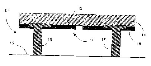
In the particular embodiment represented in figure 3, the passive
Micro bole meter 12 comprises a suspended membrane with a radiation-
absorbing element 13 and a bolometric material constituting the thermometric
element 14 of the microbolometer 12. The membrane is supported by two
anchoring elements 15 arranged on a support substrate 16. 1
The passive microboiemeter 12 comprises a reflective protective screen 17 f
t5 formed under the membrane. The protective screen 17 is formed for example
by at least one reflecting. layer 18, preferably a metallic layer, as metal
presents good radiation reflection characteristics, in particular of infrared
radia`ion, The screen 17 must be reflecting to incident radiation and must not
short-circuit the therrncmetric element 14 formed by the bolometric material.
The protective screen 17 is therefore in electrical contact with the absorbing
element 13 only and the thermometric element 14, formed by the bolometric
material, is arranged ort the absorbing element '13.
The n-aterials constit tin9 the protective screen 17 are chosen such that the
protective screen 17 presents the necessary optical and thermal properties to
reflect radiation. The layer 18 is made of metal preferably chosen from
aluminium silver gold and copper, which have an excellent infrared
retlectincl ceoscity and constitute genuine optical mir-ors. The thickness of
the metallic layer is about 500A to 2000A.
CA 02557903 2006-08-29
7
Othe` materials can be chosen for the reflecting screen 17. For example, the
screen 17 can comprise an irtrinsicaily insulating stack of layers of
materials,
in particular metals or doped indium and tin oxides.
The screen 17 can also be formed by a reflector of interferential type, i.e. a
screen comprising a stack of insulating or conducting thin layers. The screen
1 *1 can also be made from a material with surface or volume texture effect.
It
can also be made of a cerniel material, i.e. a ceramic with metal inserts,
with
a conduct ion threshold depending on the metal concentration in the ceramic.
The boiornetric material constituting the thermometric element 14 is for
example weakly or highly resistive p- or ii-type polycrystalline or amorphous
silicon The bolometric material can also be a vanadium oxide elaborated in a
serni-co-rnducting phase, a ferrite or a manganite.
The support substrate 16 is a support that is for example silicon-based. It
ensures the mechanical strength of the passive microbolometer 1 2 and
preferably comprises devices (not shown) for biasing and reading the
resistance of the thermometric element. It can also comprise multiplexing
40 components enabling, notably in the case of a detector comprising seve"al
microbolorneters with a matrix structure, the signals from the different
microholometers to be serialized and transmitted to a reduced number of
outputs to be used by a usual imagery system.
fa the particular embodiment of figure 3, the sheet resistance R. of the
absorbing element 13 trust he about 300 2 to absorb the rad;ation, For the
sheet resistance of the assen,ibly `armed by the absorbing element 13 and
the screen, 7 tc be that of a rr1flector, I.e. a sheet resistance of about 0.1
c?,
the absorbing element 13 mus be in electrical contact with the reflecting
screen 17. The sheet resistance of the absorbing element 13 is then
associated wit:i the: of the screen 17
CA 02557903 2006-08-29
The incident radiation passes through the bolometric material forming the
therrnorne'id element 14, which is transpa,ent in this embodiment, then
encounters the assembly formed by the abso~bing element 13 and the metal
screen 1 7, which then plays its role of reflecting screen, and then exits.
The
weakness of the sheet resistance of the assembly 13, 17 prevents the
radiation from being absorbed, and consequently prevents the membrane
from heating. The tt,ermornetric element 14 therefore doesn't heat and its
resistance remains unchanged.
In an alternative embodiment, not represented, the electrodes designed to
perform electrical connection between the passive microbolometer 12 and
the sJpport substrate 16 have special configurations, for example in the form
of cols, and at the same time constitute the absorbing element 13.
it e material forming the electrodes is chosen for example from titanium,
ttaniurn nitride, platinum, aluminium, palladium, nickel, nickel and chromium
alloy etc The thickness of the electrodes is about 0.005Ftm to 1 um.
In another a ternative embodiment, not represented, the bolometric material
is formed both by the thermometric element 14 and by the electrodes, for
Example in the form of a coil, and the absorbing element 13 is a separate
elernernt.
In all cases, altnough the reflecting screen 17 is arranged underneath the
membrane, the microbolorneter 12 thus obtained is passive, as its membrane
dues riot absorb radiation.
A particular embodiment of a device for thermal detection of radiation,
comprising at least one active rnicrobolonieter 19 and one passive
CA 02557903 2006-08-29
9
rnicrobolometer 12, according to figure 3, produced on a single support
substrate 16, w vili be described in. greater detail with regard to figures 4
to 7.
In figure 4.. the method for eociucing the p ddevice first comprises
successive
depositions. on the support substrate 16 bearing the anchoring elements 15,
of a sacrificial layer 20, preferably made of palyimide, of a thickness
substantia ly equal to the thickness of the anchoring elements 15 of the
r~ icrobolorneters 12 and 19, and of a metallic layer 21 constituting the
protective screen 17 of the passive microbolorneter 12.
In tigure 5, etching of the layer 21 constituting the protective screen 17
only
opposite the location, oof the active rnicrobolometer 19 enables a protective
screen 1.7 to he kept Sgt tt,e level of the passive microbolorneter 12 only.
In
the partici er emoodiment of iidur es 3 to 7, the refl~ecting screen 17 is
made
of conducting rnateriell. it is therefore indispensable to provide a
dielectric
insulation of this layer with respect to the anchoring elements 15. This
insulation is generated for example by a break in the reflecting screen 17;
achieved by etchinq, as represented in figure 3. Various layers forming the
rnembraries 22 of he rnicrcoolometers 12 and 19 are them deposited, on the
2cx acrificial layer 20 ana on the protective screen 17, arranged at the level
of
the passive rwcroboicmeter 12.
in figure 6, etching of the membranes 22 then enables the microholometers
12 anc 19 to be ~oiineated. F,nal!y, etching of the sacrificial layer 20
enables
the dstector represented in figure 7 to be obtained, with the passive
microbolcmeter 12, with 'no integrates protective screen 17, arranged
underneath the me"fnbrany 22, and the active microbolorneter 19, arranged
on the san support aubstra'_e 16.
31 in The method o` pr"oc:ucticon i"l. scribed above, the protective screen 17
i
delineated fo= example bye chc-pica! c r plasma etching proce3sea, or by a Ht-
CA 02557903 2006-08-29
off process. In the case of a metal protective screen 17, the metallic layer
18
is deposited for example by cathode sputtering, or by thermal aecomposition
(LPCVD).
5 To improve its operation, the passive m,crobolometer 12 can be thermaiized,
Le its thermal conductance be improved, by doing away with the thermal
insulation arms 6, present in particular on the active rnicrooolometer 19.
In all cases, the technology of the r ticrobolorneters 12 and 19 is not
affected
10 by Fitt ng of the reflecting screen 17, as fabrication of the reflecting
screen 17
s integrated in the fabrication process of the microbolometers 12 and 19.
This results in a saving of time and especially of cost, as the already known
rnicroholorneter production ,-re-thods and lines do not have to be changed.
is Moreover, as the detection dev cc- preferably operates in a vacuum, the
surface of the protective screen 17 in contact with the radiation does not
have to be protected by a special coating
The invention is not limited to the embodiment described above The detector
can comprise a matrix architecture enabling infrared imagery to be
pertarrned. The matrix architecture is composed of a plurality cf actve
micro holometers 19 and a plureiity of passive microbolometers 12 arranged
regularly ;n line: and columns on a single support substrate 16. The
fabrication methods are the same and the electronic measuring circuit
integrated in the support substrate 16 recovers and uses each measurement
of the microbolometers '2 and 19 to transform their into an infrared imagery.
The detector can op- encapsulated iii a vacuum or in a gas that is a very low
heat conductor, to gain performance. The enclosure in which the detector is
encapsulated then comprises a window transparent to radiation.
CA 02557903 2006-08-29
11
The -nicrobolornote rs 12, 19 of the detection device can comprise any type of
thermometric element, for example a thermistor, an electrode, a dioce, etc.