Note: Descriptions are shown in the official language in which they were submitted.
CA 02558223 2006-08-31
Flat transponder and method for the production thereof
The invention relates to a flat transponder having an
electronic circuit which is arranged in a layer or in a
layer composite and which contains at least one chip
and conductor tracks or conductor wires, and also to a
method for the production thereof.
The transponder according to the invention is suitable
for being fixed by adhesive bonding both to rigid and
to flexible elements made of paperboard, paper,
material or plastic. The preferred area of application
is the fitting of a contactless transponder in a
passport cover.
Very flat transponders are also used for many
applications in the form of contact-containing,
contactless or hybrid designs. They normally have at
least one chip, which is often arranged in a module,
and also conductor tracks or conductor wires and, if
appropriate, further electronic components.
Contactless or hybrid designs need an antenna.
It is known that these arrangements are adhesively
bonded into paper sections and also cast or laminated
into plastics, in order to secure the position of the
circuit and to avoid damage.
The protection required for these arrangements is
intended to ensure both the positional security of
their components and a certain rigidity, in order to be
able to process and test the transponders in an
automated manner.
For specific applications of these circuits, it is
necessary that they permit both secure mechanical and
electrical protection of the components and also high
flexibility. In this case, it is frequently desirable
CA 02558223 2011-10-24
2
not to disclose the position of the module in the
circuit.
A further requirement is that the arrangement may be
glued to further covering or protective layers by means
of water-based adhesives in the same way as paperboard
or paper.
Solutions are known which configure the protective
layers applied to the circuit to be extremely thin or
extremely soft, by these protective layers consisting
of very soft plastic, for example synthetic paper, and
also of woven or nonwoven material of natural or
artificial fibers.
In the case of using synthetic papers, it is
disadvantageous that these have a high thickness
tolerance and cannot be bonded with water-based
adhesives. Protective layers made of material do not
permit circuits to be protected in such a way that
dimensionally exact conditions for the circuit are
ensured. Furthermore, the position of module and chip
and/or of the electronic components can be detected by
feel or is visible in relief. It is also
disadvantageous that, although material can be
adhesively bonded very well, it is stiffened by taking
up adhesive.
The invention is based on the object of specifying a
transponder of the type mentioned at the beginning and
a method for the production thereof which is flexible,
CA 02558223 2012-05-03
3
has the most uniform thickness possible and can be
bonded to further elements by means of water-based
adhesives, its electronic components largely being
protected against damage by bending and against being
detected by feel.
According to the present invention, there is provided a flat transponder
having an
electronic circuit which is arranged in a layer or in a layer composite and
which
contains at least one chip and conductor tracks or conductor wires, the
circuit being
arranged in or on a circuit carrier (7) made of plastic, on whose two larger
opposite
outer surfaces a paper layer (6) applied by lamination is in each case
applied,
characterized in that notches (11) are introduced into at least one paper
layer (6) in
order to increase a flexibility and that the notches (11) are applied at
different
intervals or with a different depth on the various sections of the paper layer
(6) in
order to create surface regions of different flexibility or different
flexibility directions.
According to the present invention, there is also provided a flat transponder
having
an electronic circuit which is arranged in a layer or in a layer composite and
which
contains at least one chip and conductor tracks or conductor wires, the
circuit being
arranged in or on a circuit carrier (7) made of plastic, on whose two larger
opposite
outer surfaces a paper layer (6) applied by lamination is in each case
applied,
characterized in that notches (11) are introduced into at least one paper
layer (6) in
order to increase a flexibility and that the notches (11) are applied at
different
intervals or with a different depth on the various sections of the paper layer
(6) in
order to create surface regions of different flexibility and different
flexibility
directions.
According to the present invention, there is also provided a flat transponder
having
an electronic circuit which is arranged in a layer or in a layer composite and
which
contains at least one chip and conductor tracks or conductor wires, the
circuit being
arranged in or on a circuit carrier (7) made of plastic, on whose two larger
opposite
CA 02558223 2012-05-03
4
outer surfaces a paper layer (6) applied by lamination is in each case
applied,
characterized in that notches (11) are introduced into at least one paper
layer (6) in
order to increase a flexibility and that the notches (11) are applied at
different
intervals and with a different depth on the various sections of the paper
layer (6) in
order to create surface regions of different flexibility or different
flexibility directions.
According to the present invention, there is also provided a flat transponder
having
an electronic circuit which is arranged in a layer or in a layer composite and
which
contains at least one chip and conductor tracks or conductor wires, the
circuit being
arranged in or on a circuit carrier (7) made of plastic, on whose two larger
opposite
outer surfaces a paper layer (6) applied by lamination is in each case
applied,
characterized in that notches (11) are introduced into at least one paper
layer (6) in
order to increase a flexibility and that the notches (11) are applied at
different
intervals and with a different depth on the various sections of the paper
layer (6) in
order to create surface regions of different flexibility and different
flexibility
directions.
According to the present invention, there is also provides a method for the
production of the transponder, characterized in that the circuit is fitted in
or on a
circuit carrier (7) made of plastic and in each case a paper layer is applied
to both
sides of the circuit carrier (7) by hot lamination and in that notches are
applied on at
least one surface side of the laminate, wherein said notches are applied at
different
intervals and/or with a different depth on the various sections of the paper
layer in
order to create surface regions of different flexibility and/or different
flexibility
directions.
Preferably, the transponder contains a circuit which is arranged in an
electrically
insulating, flexible and water-resistant plastic element. A covering layer
made of
paper or a material similar to paper is laid onto the plastic element on one
or both
sides and fixed by lamination. In the sense of the invention, paper is
understood to
CA 02558223 2012-05-03
4a
mean a sheet material which has predominantly been produced of natural fibers
of
different origin. One or both covering layers and, if appropriate, the partial
layers of
plastic arranged adjacently above it or under it are notched with incisions,
so that
the intrinsically stiff laminate with the circuit located in the interior of
the laminate
bends over at the notched points under bending loading, even with relatively
low
forces. The notches may be produced by drawn or punched incisions using
special
knives, by grinding, by sawing in, by laser cutting, etc.
Preferably, a further possible way of producing the notches is to provide the
laminating rolls or laminating plates needed for the laminating process with
elevated, knife-like notching webs so that, with the lamination process, the
notches
are already pressed or cut into the laminate produced. In addition, a first
notch
pattern can be notched in with the lamination, and a second notch pattern can
be
notched in by means of additional notching following the lamination.
Preferably, the notch depth and the notch cut density can be applied
differently for
regions of the laminate surface. In order not to be able to detect the module
or chip
in the laminate by feel and to prevent the conductor wires or conductor tracks
from
bending over at the module or chip connection, it is expedient not to
flexibilize the
regions surrounding the module or chip or to flexibilize them only slightly,
in order
additionally to make detecting the module or chip by feel more difficult.
Furthermore, still preferably, it is expedient to configure the notch cuts in
accordance with specific patterns, which permit identification and therefore
ensure
additional security against the simple plagiarization of the laminate. The
patterns
can represent specific lines, actual symbols, dot patterns and the like. In
specific
regions of the laminate, restricted in terms of their area, notching through
or
perforation is advantageous. When using grinding methods or laser cutting
methods
for producing the notches, it is possible to configure the cross section of
the notches
CA 02558223 2012-05-03
4b
(width and opening angle) specifically as a security feature and/or in order
to
predefine a specific bending behavior, at least in one surface region of the
laminate.
The laminates exhibit high evenness, a low thickness
tolerance, high compressive strength and optimal
mechanical protection of the module, chip, electronic
components and conductor tracks or conductor wires.
The laminates can be bonded with water-based adhesives.
The invention will be explained in more detail below by
using exemplary embodiments.
In the associated drawing:
figure 1 shows a contactless transponder in plan view,
figure 2 shows a contactless transponder in cross
section,
CA 02558223 2006-08-31
figure 3 shows a plan view of an arrangement having
notches, and
figure 4 shows the arrangement having notches in cross
5 section.
The arrangement illustrated in figure 1 shows a
laminate 1 having a surface similar to a check card.
Arranged in the laminate 1 is a module 3, whose module
connections 4 are connected at the contact points 5 to
the ends of the antenna 2. The antenna 2 comprises a
coil having two turns of copper wire provided with an
electrically insulating layer and having a diameter of
50 pm.
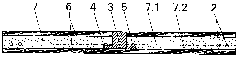
In figure 2, the laminate is shown in cross section.
The antenna 2 is located in a circuit carrier 7 which,
in the example, comprises a 200 pm thick upper plastic
film 7.1 and a lower plastic film 7.2. Those films
consist of polyethylene. Located on the upper plastic
film 7.1 are the antenna 2 and the module connections 4
connected to the antenna 2 at the contact points 5.
The thermosetting, rigid body of the module 3 is
arranged in a hole which has been punched through the
circuit carrier 7 and the paper layer 7 located above.
Applied under the upper plastic film 7.1 is the lower
plastic film 7.2, which is 100 pm thick in the example.
A second paper layer 6 is arranged underneath the lower
plastic film 7.2, so that the plastic films 7.1 and 7.2
are each covered by a 100 pm thick paper layer 6.
To produce the transponder, the material layers laid
together one above another become a compact composite,
the laminate 1, by means of hot lamination. Here, the
conductor wires 2 are located between the two plastic
films 7.1 and 7.2. During the lamination process, the
plastic films 7.1 and 7.2 consisting of polyethylene
temporarily soften. In the process, they bond to each
other and to the paper layers 6. In the example, the
CA 02558223 2006-08-31
6
paper layers 6 consist of paper of the stiff grade
"coated paper". The stiff paper layers 6 on the outer
sides of the laminate 1 prevent the polyethylene core
consisting of the plastic films 7.1 and 7.2 from
shrinking during the lamination and significantly
changing the position of the conductor tracks or
conductor wires 2 forming the antenna 2. By means of
the non-shrinking paper layers 6 to which the plastic
films 7.1 and 7.2 are fused, positional stabilization
of the electronic circuit and of the entire plastic
core is achieved. This positional stabilization can be
achieved for virtually all plastics to be laminated.
The paper layers 6 consisting of coated paper
additionally prevent the plastic films 7.1 and 7.2 that
soften during the lamination from impregnating the
fiber composite of the paper layers 6 completely. For
this arrangement, the impregnation is not desired,
since a paper completely impregnated with polyethylene
- complete integration cannot be avoided in the case of
thin, uncoated papers - cannot be bonded by means of
water-based adhesives or can be bonded only very
poorly. Furthermore, depending on the level of
impregnation of the uncoated paper by the plastic films
7.1 and 7.2 to be laminated in the composite, the
thickness of the laminate 1 fluctuates very
considerably, since some of the plastic compound is
taken up by the paper layers 6. On the other hand,
stiffening of the layer composite results from the
lamination, which is normally not desired.
In order to obtain flexible laminates 1 despite
lamination, the outer paper layers 6, which contribute
significantly to the stiffening, are provided with
notches 11 illustrated in figure 3. The notches 11 are
primarily implemented in the left and right edge region
of the laminate 1 in close cut patterns in order to
increase the flexibility. The edge regions therefore
become regions of lower flexural rigidity 10.
CA 02558223 2006-08-31
7
Regions of high flexural rigidity 9 are arranged in the
center of the laminate. To this end, the region around
the module 3 has no notches 11, in order to prevent the
laminate 1 from being able to be bent over directly at
the module 3. In addition, two further areas similar to
a module are implemented without notches 11, in order
that simple detection of the exact position of the
module 3 by feel is not possible. Furthermore, two
special symbols 8 are notched in the vicinity of the
lower edge of the laminate 1, permitting individual
identification of the laminate 1 and/or the batch with
a producer's identifier, the date of production and the
like.
In the example illustrated, the notches 11 are arranged
in the manner of diamonds but, depending on the desired
flexibility of the laminate 1, depending on the
technological possibilities and depending on the design
wish, other notch arrangements are possible. For
example, the notches 11 can be made in the form of
waves, overlapping ring forms, any desired polygonal
forms and so on. In the example, the notch cuts 11
have been produced by means of a CO2 laser following
the lamination.
Figure 4 explains possibilities of various types for
the application of notches 11 to the laminate 1. Both
surface sides of the laminate 1 have been provided with
notches 1, each surface side having different notches
corresponding to the flexibilities required for the
respective bending directions. To this end, deep V-
shaped notches 11.1 can be applied in specific regions
and shallow V-shaped notches 11.3 can be applied in
other regions.
Furthermore, it is possible to arrange the notches 11
as through notches 11.2 or in the form of a trench cut
11.4. In figure 4, the upper side of the laminate 1
CA 02558223 2006-08-31
8
has V-shaped notch cuts, which are arranged at the
edges of the laminate 1 at reducing intervals and as
deep V-shaped notches. In the center of the laminate 1,
shallow V-shaped notches 11.3 have been made. The
shallow V-shaped notches 11.3 notch only the paper
layer 6. At the edge of the laminate 1 there are deep
V-shaped notches 11.1, which notch the paper layer 6
and about 30% of the thickness of the circuit carrier
7. On the lower surface side of the laminate 1, trench
cuts 11.4 have been introduced, which notch only the
paper layer 6. For particular identification, the
laminate 1 is provided with dot-like through notching
11.2 on the left side.
CA 02558223 2006-08-31
- 9 -
LIST OF DESIGNATIONS
1 Laminate
2 Antenna
3 Module
4 Module connection
Contact point
6 Paper layer
7 Circuit carrier
7.1 Upper plastic film
7.2 Lower plastic film
8 Special symbol
9 Region of high flexural rigidity
Region of low flexural rigidity
11 Notches
11.1 Deep V-shaped notch cut
11.2 Through notch
11.3 Shallow V-shaped notch cut
11.4 Trench cut