Note: Descriptions are shown in the official language in which they were submitted.
CA 02558461 2006-09-O1
WO 2005/091949 PCT/US2005/006902
METAZZIZATION PROCESS AND PRODUCT PRODUCED THEREBY
CROSS REFERENCE TO RET~ATED APPZICATION
This application claims the benefit of the filing date of
Unite d States Application No. 10/794,482 filed March 5, 2004, the
disci osure of which is hereby incorporated herein by reference.
BACKGROUND OF THE INVENTION
The present invention relates generally to the metallization
of a substrate utilizing a transfer film, either in a selective
l0 or non-selective metallization process. More particularly, the
present invention relates to such metallization processes, which
include a protective coating over the metallized substrate during
the rnetallization step, rather than as a separate procedure.
Aspects of the invention also focus on an intermediate product
l5 formed from a transfer film, coating, a . g. , a cured coating, and
metal layer used in the transfer process. Additionally, the
present invention relates to the resulting metallized substrate.
Processes for the metallization of various substrates have
been known for some time. These methods are typically a two-step
20 process. The first step is to create a transfer mechanism. The
transfer mechanism typically comprises a transfer film, or
carrier, coated with a lacquer release layer. Metallic particles
are then deposited onto the lacquer release layer by conventional
methods such as vacuum deposition. In the second step, adhesive
25 mater ia1 is applied to a substrate whereupon the transfer
mechanism is adhered, with the metallic layer adjacent the
adhesive coating. After heating the various elements, the
carrier layer is removed to reveal a metallic-coated substrate
having a lacquered protective layer. In conventional terms, this
30 process is known in the art as "hot stamping." While hot
stamping is beneficial for some uses, it only enjoys limited
applicability.
Hot stamping may not be used with all substrates, as the
heatZng process may be destructive. Also, it has been found that
35 the hot stamped foil may separate from the substrate under
aggressive conditions, if not under normal use. Such separation
CA 02558461 2006-09-O1
WO 2005/091949 PCT/US2005/006902
2
is undesirable as it compromises the integrity of the finished
product. Hot stamped metallic foils are also not print able.
U.S. 4,473,422 (H. Parker et al., issued Sept. 25, 1984)
discloses more advanced techniques for metallizing a substrate
have subsequently been developed and are generally kn own in the
art. One such method is to provide a transfer fit m having a
coating layer and metallic layer on the film much like that of
the hot stamping process. This three-part transfer film may then
be adhered to a substrate using a pressure sensitive adhesive.
Once the adhesive is cured, the film may be removed t o reveal a
substrate/ adhesive/ metal/ coating product. For purposes of the
present invention, the designation a/b/c/d, etc., s s used to
describe various products, structures or constructions where "a"
is the base layer and "b, " "c, " "d, " etc. are succes sine layers
of materials. Techniques of this type do not disclose the use of
a 1000 solids-containing, electron beam (EB) curable adhesive.
As such, the substrate must be porous to permit a mean s of escape
for the moisture or diluent contained in the uncured adhesive.
In addition, this technique does not permit the selective
metallization, or metallization in discontinuous regions, of the
substrate. Rather, the metallization process must b a conducted
in a continuous sheet.
Other processes for nonselectively metallizing a substrate
are also known. In one of these processes, U.S. 4,90,409 (S.
Nablo, issued Dec. 25, 1984), a film is coated with a release
coat adhesive and a prime coat protective coating. A metal layer
is adhered to an electron beam radiation sensitive substrate,
e.g., paper, with an adhesive. The various adhesive and the
coating layers may be EB curable. When the film is re moved after
curing the release coat adhesive, prime coat protective coating,
and metal layer adhesive, the release coat adhesive remains
adhered to the film, leaving the prime coat protective coating as
a layer above the metal. The final result is a substrate/
adhesive/ metal layer/ protective coating system.
Processes for the selective metallization of a substrate are
also known. One such process, U.S. 6,544,369 (Y. Kitamura et
CA 02558461 2006-09-O1
WO 2005/091949 PCT/US2005/006902
3
al., issued April 8, 2003), utilizes a two-part transfer film in
its first step. The two-part transfer film comprise s metal
deposited directly onto a plastic film using conventional
methods. No coating layer or prime coat is adhered to the
transfer film between the metal and the plastic film. A
substrate is then introduced. Either the substrate or the metal
side of the transfer film is selectively coated with an
EB-curable adhesive. The substrate and the transfer film are
then brought together and the adhesive is EB cured. The plastic
film is then removed. The finished product is a
substrate/adhesive/metal product. Of note, the metal 1 ayer of
structures resulting from techniques of this type is exp used to
the atmosphere, and not protected by a separate coating. Methods
to improve this result are disclosed in the same reference.
One such method is to coat the metal in a completely
separate second process. In this process, a curable resin of a
solvent type, aqueous type, and water soluble type, is described
and may be applied to a transfer film. This two-part film may
then be covered over the substrate/adhesive/metal product of the
prior technique. Once the resin is cured, removal of t he film
reveals a protected, selectively metallized substrate. Although
the selectively metallized substrate is protected, the pro tection
covers the entire substrate and not merely the selectively
metallized portion. This presents limitations, as the areas
which are not metallized, but which are protected, may suffer
from undesired effects, such as reduced sharpness or color
brightness, among others.
Notwithstanding these teachings, it would be advantageous to
provide for the selective metallization of a substrate wh ere the
finished product comprises a substrate/adhesive/metal/ coating
system in a one-step process, particularly wherein the transfer
film mechanism has been cured prior to curing of the adhesive.
Furthermore, it would be desirable to produce a met allized
structure in which the metallized portions, whether t o tal or
selective, have a well-defined, e.g., sharp or precise,
separation from the non-metallized portions.
CA 02558461 2006-09-O1
WO 2005/091949 PCT/US2005/006902
4
SUMMARY OF THE INVENTION
An embodiment of the invention provides a layered structure
comprising at least one each of: (a) a substrate layer; (b) a
metal-containing layer; (c) an adhesive-containing layer adhering
said metal in said metal-containing layer to said substrate
layer; and (d) a breakaway layer, having a top surface and a
bottom surface, said bottom surface of said breakaway layer
coating substantially only said metal of said metal-containing
layer. A further embodiment provides a metallized structure
having selectively metallized areas. In accordance with one
embodiment of the invention, there is disclosed a layered
structure comprising at least one each of: (a) a substrate layer;
(b) a metal-containing layer; (c) an adhesive-containing layer
adhering said metal in said metal-containing layer to said
substrate layer; and (d) a breakaway layer, having a top surface
and a bottom surface, said bottom surface of said breakaway layer
coating substantially only said metal of said metal-containing
layer. In another embodiment the breakaway layer has a cured
elongation at break when tested in tension of less than about
20 0 .
In yet another embodiment there is provided a method of
metallizing a substrate comprising the steps of: (a) providing a
transfer film comprising a film layer and a metal layer bonded
together by a cured breakaway layer; (b) providing a substrate;
(c) applying an electron beam curable transfer adhesive to at
least a portion of said substrate; (d) securing said transfer
film to said substrate comprising said transfer adhesive such
that said transfer adhesive is disposed between said metal layer
and said substrate to form an intermediate product; (e) passing
said intermediate product through an electron beam curing
apparatus to cure said transfer adhesive; (f) removing said
transfer film from said intermediate product to provide a
metallized substrate product having a cured breakaway layer
bonded to said metal layer at said transfer adhesive portion. In
a still further embodiment, there is disclosed a method of
metallizing a substrate wherein the cured breakaway layer has a
CA 02558461 2006-09-O1
WO 2005/091949 PCT/US2005/006902
cured elongation at break when tested in tension of less than
about 200.
In other embodiments the structure is either totally or
selectively metallized. The invention provides for structures
5 having precise or sharp metallized edges, e.g., a metallized edge
varies from a line drawn along the edge and mid-way through the
variations from the line by less than or equal to about ~ 0.010
inches.
BRIEF DESCRIPTION OF THE DRAWINGS
The subject matter regarded as the invention is particularly
pointed out and distinctly claimed in the concluding portion of
the specification. The invention, however, both as to
organization and method of operation, together with features,
objects, and advantages thereof may best be understood by
reference to the following detailed description when read with
the accompanying drawings in which:
Fig. 1 is a cross-sectional view of a transfer film in
accordance with a preferred embodiment of the present invention;
Fig. 2 is a cross-sectional view of an intermediate product
in accordance with a preferred embodiment of the present
invention;
Fig. 3 is a cross-sectional view of a selectively metallized
substrate in accordance with a preferred embodiment of the
present invention; and,
Fig. 4 is a schematic view of a method of selectively
metallizing a substrate in accordance with a preferred embodiment
of the present invention.
DETATLED DESCRIPTION
In describing preferred embodiments of the subject matter
illustrated and to be described with respect to the drawings,
specific terminology will be resorted to for the sake of clarity.
However, the invention is not intended to be limited to the
specific terms so selected and it is to be understood that each
specific term includes all technical equivalents which operate in
a similar manner to accomplish a similar purpose.
CA 02558461 2006-09-O1
WO 2005/091949 PCT/US2005/006902
6
In this regard, the term "film" or "carrier" shall broadly
be construed as a thin and flexible sheet. The films utilized
must have qualities such that a desired breakaway coating or
layer of the invention adheres to the film, but that the affinity
of the coating for the film is less than that of the breakaway
coating's affinity for metal deposited on the breakaway coating.
Suitable materials for the film or carrier include acetate;
cellophane; polypropylene; polyethylene; polyester; polystyrene;
holographic or diffraction films; clear, dyed, filled or coated
films; mat finished films; metallized, full or patterned films;
microwave and susceptor film; and treated film such.as corona or
chemically treated film. Mixtures of polymers having film-
forming properties can also be used. Other than the suitable
adhesion and release qualities as just described, the carrier
film properties are not critical to the final construction or
structure since the carrier film will not be an integral part
thereof .
Useful film typically has a thickness of about 0.18 mil to
about 4.0 mil; for example, from about 0.25 mil to about 2.5 mil;
alternatively, about 0.5 mil to about 1.5 mil. If desired, the
film may be dyed or colored with suitable materials. The film
may also be embossed or patterned to produce a further surface
effect on the final product.
As used herein, the term "coating" or "breakaway coating" is
defined as at least one layer that is between the (carrier) film
and a metal layer. The breakaway coating functions as an
adhesive layer in that, in addition to other properties and
characteristics described herein, including acting as a
protective layer and as a printable layer, it adheres to the
metal layer and, at least temporarily, to the carrier film layer.
As a consequence of the process of the invention used to form the
metallized structure, the metal present in the metal layer can be
in the form of contiguous metal-containing areas or areas
separated by non-metallized areas; in each instance, the
breakaway coating is present only on the metallized portions of
the metal-containing layer. Furthermore, it will be appreciated
CA 02558461 2006-09-O1
WO 2005/091949 PCT/US2005/006902
7
that the breakaway coating layer may be formed of either a single
layer of material or of multiple layers of material. Such
multiple layers may be of the same composition or may vary in
composition from each other. In an alternative embodiment, the
coating layer comprises at least two layers. Application of a
second, and subsequent, layer can be employed to cover pinholes,
or localized areas where coverage of the initial layer is
considered to be inadequate. The composition of the breakaway
coating layer used in the present invention generally comprises
acrylates; urethane acrylates; epoxy acrylates; polyester
acrylates; acrylate acrylics and other oligomers and polymers
having suitable properties as further defined herein. For
purposes of the present invention, the terms oligomer and polymer
have their standard or accepted meanings in the art. For
example, an oligomer is understood to be a polymer molecule
comprising only a few monomer units, e.g., dimer, trimer,
tetramer, etc., but can include as many as ten, twenty or more
units since a precise upper limit is not fixed.
For purposes of the present invention, the breakaway coating
must release from the carrier film and adhere to the metal
present in the metal-containing layer in those areas in which the
metal of the metal-containing layer is adhered via the transfer
adhesive to the final product substrate. Release from the
carrier film can be measured using, for example, an Instron~
tester using a ~ inch long by 1 inch wide test strip of the
carrier film to which a layer of the breakaway coating has been
applied. A piece of #600, 3M Scotch Brand tape is tightly
adhered to the coating layer and a free end of the tape is held
in one jaw of the tester while the coated film is held in the
other jaw. As the jaws are separated at a rate of 1 ft./min.,
the force required to pull the coating layer off of the film is
measured. Typically, the breakaway coating will exhibit a
maximum release strength of less than about 30 grams/inch;
preferably about 2.0 to about 25.0 grams/inch; more preferably
about 3.0 to about 15.0 grams/inch; most preferably about 3.5 to
CA 02558461 2006-09-O1
WO 2005/091949 PCT/US2005/006902
8
about 10.0 grams/inch; for example, about 3.5 to about 8.0
grams/inch.
In a particularly preferred embodiment of the invention, the
breakaway coating exhibits a low level of elongation when
stressed in tension. Consequently, the breakaway coating can be
characterized as relatively rigid, tending to fracture under
stress rather than exhibiting significant elongation. As will be
further described in detail below, such fracture results in a
desirable fine, precise or sharp, line of demarcation between the
metallized and non-metallized areas due to the high adhesion of
the metallized areas to the product substrate via the transfer
adhesive. The elongation characteristic of the breakaway coating
can be determined using a cured sample of the breakaway coating
and following ASTM Method D882 for a material having a thickness
of less than about 1.0 mm (0.04 in.) and ASTM Method D638-02a for
any thickness up to about 14 mm (0.55 in.). Suitable test
conditions are as follows: a test instrument such as an Instron
tensile tester is used with the test sample mounted in the
vertical direction; temperature, humidity, sample length, width
and thickness should be selected and kept constant consistent
with good laboratory test practices. Similarly, sample extension
rate should be kept constant according to the test method, a . g. ,
a suitable extension rate is about 0.1 to about 1 mm/min.; a
convenient extension rate can be selected based on the properties
of the particular breakaway composition. Separation of the test
grips should be about 100 mm and the sample size at least 50 mm
longer than the grip separation used; sample width can vary
between about 5mm and about 25mm, but it should be at least 8
times the sample thickness. Sample preparation can conveniently
be conducted using a smooth substrate that allows for good flow
of the breakaway coating before it is fully cured, but low
adhesion so that the coating is not distorted or fractured prior
to testing. Suitable substrates or surfaces include smooth,
polished mild steel and release paper such as silicone release
paper. After the breakaway sample is fully cured according to
the conditions suitable for the chemical composition of the
CA 02558461 2006-09-O1
WO 2005/091949 PCT/US2005/006902
9
coating, test samples can be die cut or out from the cured
composition using, e.g., a sharp knife or scalpel and a straight
edge, e.g., a metal rule.
Suitable compositions for use as a breakaway coating in the
present invention will have a cured elongation at break when
tested in tension, as follows: (1) for use in selectively
metallized structures, elongation at break that is typically
about zero to less than about 200; preferably about 0.5o to about
150; more preferably about 0.750 to about 10%; for example, about
1o to about 80 or zero to about 80. For purposes of the present
invention, it should be understood that "zero" percent elongation
includes values that are only slightly greater than zero and
within experimental error of zero in view of the measuring
capability of the test equipment used to measure this property.
Consequently, if a sophisticated, high sensitivity instrument not
typically used for general-purpose testing, would be capable of
measuring an elongation value of about 0.4o to about 0.10 or
lower, e.g., 0.010 or lower, such values are, for convenience,
referred to herein as "zero." Alternatively, such materials are
characterized as brittle, in contrast to elastomeric or plastic,
wherein elongation at break in tension for elastomeric or plastic
compositions can be, e.g., about 1000, 1500, 200% or greater.
(2) Breakaway layer compositions useful in metallized structures
where the metal present in the metal-containing layer is
substantially totally transferred, elongation at break that is
typically about 1000 to less than about 300%; preferably about
1000 to about 2000; more preferably about 1050 to about 1750; for
example about 1200.
Useful oligomer and polymer compositions for the breakaway
coating or layer of the present invention comprise at least one
component selected from the group consisting of urethane acrylate
resin; polyurethanes, including aliphatic and aromatic
polyurethanes and mixtures; polyesters; cellulose derivatives,
including cellulose acetate, cellulose acetate butyrate and
nitrocellulose; acrylics; and mixtures thereof. The composition
is preferably a urethane aerylate resin. The proportion of each
CA 02558461 2006-09-O1
WO 2005/091949 PCT/US2005/006902
component in, e.g., a urethane acrylate resin can be selected,
with limited experimentation, in order to achieve usable as well
as preferred elongation and release properties described above.
For example, higher acrylate content would tend to have more
5 adhesive characteristics and, if too high, could adhere
unacceptably to the carrier film. Conversely, a higher level of
urethane will more readily release from a polyester carrier film,
but too high a urethane content may result in excessive
elongation, depending on the character of the urethane selected
10 and the type of metal transfer desired, i.e., selective or total.
Given the property guidelines above, a broad range of oligomers
and polymers can be selected for use in combination with the
carrier film as well as the transfer adhesive layer and
substrate, discussed hereinbelow.
The breakaway film, coating or layer is ordinarily applied
as a liquid or fluid. The typical composition of the present
invention can be applied as a water or solvent borne composition;
useful solvents include methyl ethyl ketone, esters such as ethyl
acetate and isopropyl acetate. Aliphatic solvents such as hexane
or heptane and aromatics such as benzene or toluene typically are
not used. The breakaway coating undergoes curing, e.g., with or
without the application of heat, in order to fully cure, for
example, substantially fully cure, to a rigid or brittle
material, as described above. The breakaway coating of the
present invention is typically oven dried to effect cure; useful
curing temperatures are about 100 °F to about 500 °F; preferably
about 200 °F to about 400 °F; most preferably about 250
°F to
about 350 °F. Useful commercial materials for purposes of the
present invention include Grancoat~ 571, 1012 and 8520 (Grant
Industries, Inc.) as well as Solucote~ 1091, an aliphatic
polyurethane, water borne dispersion (Soluol Chemical Co., Inc.).
It may also be suitable to employ a urethane acrylate or other
oligomer/reactive diluent resin composition that is susceptible
to radiation curing, e.g., using electron beam (EB) radiation
curing, provided that the above-described suitable elongation and
carrier release properties can be obtained. Furthermore,
CA 02558461 2006-09-O1
WO 2005/091949 PCT/US2005/006902
11
depending on the properties desired and the esthetic
characteristics of the resulting structure, there can be
incorporated into the breakaway layer additional materials,
including fillers, dyes and pigments.
When the breakaway coating is applied to the underlying
metal-containing metal layer, and when the final product
structure is produced, including the substrate and transfer
adhesive, the top surface of the breakaway layer of the present
invention has a desirable surface finish as a consequence of
using the materials and obtaining the properties as taught
herein. Various surface finishes can be achieved, including a
mirror finish, a matte finish, a hairline pattern finish, an
embossed pattern finish, a hologram pattern finish and mixtures
or combinations of these finishes.
As used herein, the term "transfer adhesive," means a
component, composition or material applied as a layer between the
substrate and the metal-containing metal layer in order to secure
or bond the substrate and metal layers to one another. Typical
transfer adhesives comprise at least one component selected from
the group consisting of urethane acrylate resin; epoxy acrylate
resin; polyester acrylate resin; mono- di-, tri-, or tetra-
hexacrylate resin; and mixtures thereof. Preferably, the
transfer adhesive comprises a urethane acrylate resin; more
preferably the transfer adhesive, including a urethane acrylate
resin, is radiation curable, preferably using electron beam (EB)
radiation. Electron beam radiation units useful in the present
invention are readily available and typically consist of a
transformer capable of stepping up line voltage to the required
levels and an electron accelerator. The EB radiation initiates
the formation of radicals or rations, sometimes enhanced by the
use of initiators and other additives known in the art. The
result is that the oligomers or polymers susceptible to radiation
curing undergo cure. For purposes of the present invention the
term "cure" is used with reference to oligomers, polymers,
resins, adhesives, etc., useful in the present invention that can
be thermally cured as well as those that can be cured by EB
CA 02558461 2006-09-O1
WO 2005/091949 PCT/US2005/006902
12
methods. Furthermore, for purposes of the present invention,
"cure" means that such oligomers, polymers, and/or other
materials referred to above or hereinafter, solidify, dry, set,
harden, polymerize and/or crosslink, as is appropriate for the
material employed. The term "full cure" or "fully cured" does
not require, e.g., that the oligomer, polymer or resin, cure to
the extent that no further curing reactions are possible, but
merely to the point of practical utility; i.e., that the
oligomer, polymer or resin has reached a condition where its
physical properties are useful for the purposes intended herein.
Alternatively, regarding materials that cure or set by drying,
typically thermally assisted drying, the curing process removes a
diluent or solvent present in the composition in order to effect
the desired increased strength and/or brittleness. Regarding
polymers capable of being cured by crosslinking, such polymers
typically are considered to be fully cured when they achieve
approximately 90% of the maximum modulus or tensile strength that
they would achieve if the curing process was allowed to continue.
Reaction time for EB curing can be extremely fast, e.g., in as
little as about 0.1 seconds to about 10 seconds; although other
processing variables may dictate the use of particular cure
times. Furthermore, a transfer adhesive can further include at
least one additive selected from the group consisting of fillers,
dyes and pigments. Such additives can find utility for modifying
the processing or final properties of the adhesive composition
and its performance in the layered structure.
Useful EB curable resins include those made by Akzo Nobel
Resins under the brand name Actilane~ and including aromatic
urethane acrylates, aliphatic urethane acrylates, epoxy
acrylates, and polyester acrylates having various degrees of
functionality, e.g., difunctional, trifunctional, etc. Radiation
curable epoxy and urethane acrylates are also available from
Sartomer Company, Inc. under various "SR" grade designations. A
useful publication reports the performance properties of a broad
range of compositions from which suitable materials can be
selected; see Urethane Acrylates: Expansion of Radiation Curable
CA 02558461 2006-09-O1
WO 2005/091949 PCT/US2005/006902
13
Epoxy Acrylate Coatings, H.C. Miller, presented at Radtech '89-
Europe, Qct. 9-11, 1989. Compositions having elongation values
ranging from about 5o to about 50o are illustrated. Also useful
are EB curable adhesives manufactured by Sun Chemical Co.,
including, for example, Sun Chemical~ 7573, an aromatic urethane
acrylate copolymer having a 50/50 weight ratio of urethane to
acrylate (Sun Chemical Corporation).
The metal layer, typically in the form of a foil, is
deposited by conventional methods such as vapor deposition or
vacuum metallization. For purposes of the present invention, the
term "metal layer" means the layer of the structure containing
metal since it is not necessary that the metal be present
throughout the metal layer. Consequently, this layer is more
accurately defined as a "metal-containing" layer since metal may
be present throughout the layer or only in selected portions
depending on the desired appearance of the resulting structure.
The manner in which total or selective portions of the
metal-containing layer are metallized is described in detail
below. The term "metal" is defined in the usual manner as any of
various opaque, fusible, ductile and typically lustrous
substances that are good conductors of electricity and heat.
Typical metals form salts with non-metals, basic oxides with
oxygen, and alloys with one another. For purposes of the present
invention, the term metal also includes the various alloys
thereof. Thus, a substance comprising two or more metals or of a
metal and a non-metal intimately united, usually by being fused
together and dissolved or dispersed in each other when molten,
shall also be included in the definition of a metal. The metal
layer of the present invention includes at least one metal. Some
examples of metals that may be utilized in this invention are
aluminum, silver, gold, platinum, zinc, copper, nickel, tin,
silicon, and alloys and mixtures thereof. Deposition of the
metal layer is accomplished by methods well-known in the art,
including, e.g., vacuum deposition, sputtering, etc.
The thickness of the metal layer can vary depending on the
visual effect desired. For example, thickness typically varies
CA 02558461 2006-09-O1
WO 2005/091949 PCT/US2005/006902
14
from about 20 angstroms (A) to about 1000A; alternatively, the
thickness can be selected from the group consisting of about 30A
to about 800A: about 40A to about 600A; about 50A to about 400A;
about 55A to about 300A; about 60A to about 200A; and about 25A
to about 150A. Useful metal coatings can also be obtained at
thicknesses of about 100 A to about 600 A; alternatively, about
150 A to about 500 A; f or example, about 125 A to about 450 A.
Furthermore, useful thic knesses of the metal present in the metal
layer can be defined according to the optical density of the
deposited metal. Typically, optical density is greater than
about 1.5 to about 1.8; for example, about 2.0 or more, e.g., 3.0
or more. As optical density of a metal layer increases, the
light transmission through it decreases. For example, an
industry standard relating to digital video or versatile discs,
DVDs, typically made of polycarbonate coated with a metallic
coating, known as DVD 10, typically has an optical density of
between 2 and 3, equivalent to only 0.1 to 0.3o transmission. It
is recognized that materials with an optical density greater than
1.5 can be challenging t o photocure, e.g., using UV curing. See,
Published U.S. Application 2002/0066528, incorporated herein by
reference in its entire ty. Generally, the thickness of a metal
layer can be determine d, e.g., using an electron microscope or
with surface resistivity measurements. The literature provides
an estimate of the relationship between optical density of a
metal film and its thickness, for example with regard to an
aluminum film. Based on data for an aluminum layer exhibiting a
surface resistance of 0.80 to 1.80 ohms per square and the
relationship between film thickness and surface resistivity, the
thickness of such a layer deposited at an optical density of 2 is
estimated to range from 147 A to 331 A. See E. Mount, Converting
Magazine, Sept. 2002; and Section 2: "Electrical, Optical and
Metal Thickness Relationships," Metallizing Technical Reference,
3rd Ed., E.M. Mount III Editor, Assn, of Industrial Metallizers,
Coaters and Laminators, 2001; each reference incorporated herein
in its entirety. The present invention is not limited to
exceptionally thin met al layer thicknesses since curing of the
CA 02558461 2006-09-O1
WO 2005/091949 PCT/US2005/006902
breakaway layer and the adhesive-containing layer is preferably
accomplished by, e.g., drying, thermal and electron beam curing
methods, as described below in detail. In contrast, in order to
use UV curing to cure compositions useful in, e.g., the breakaway
5 and/or adhesive-containing layer, a very thin layer of metal is
required in order to permit a sufficient amount of UV radiation
to penetrate the metal layer and effect cure. Consequently,
while the present invention excludes the use of UV radiation
curing and its inherent limitations, the invention can
10 advantageously use EB curing as well as utilize appropriate metal
and breakaway layer thicknesses required for a particular
application.
For purposes of the present invention, the term "substrate"
means any underlying layer that forms the final product,
15 structure or construction comprising the several layers described
above. Typically, this underlying layer will be the base layer
of the finished product. However, this need not be the case if
other arrangements are desired. The substrate can be produced in
a form selected from the group consisting of board, sheet, film,
woven fabric and non-woven fabric. Typical substrates used in
this invention include, but are not limited to coated and
uncoated papers and board made from natural pulp, synthetic pulp
or mixtures thereof; natural or synthetic fibers, synthetic or
plastic papers, for example those made from polypropylene or
polyethylene, paper comprising polymeric fibers; resin or
polymeric films or other structures, e.g., card stock, based on
polymers such as polypropylene, polyester, polyethylene,
polycarbonate, acrylic, polyimide, polyvinyl chloride,
polystyrene, cellophane, polyethylene terephthalate, ethylene-
vinyl alcoholate, polyacrylonitrile, cellulose acetate butyrate,
nylon or polyamide, polyvinyl alcohol, ethylene-vinyl acetate,
polyurethane, polymethyl methacrylate, polylactic acid and
polycaprolactone; latex impregnated papers; non-woven fabric made
from pulp synthetic resin, biodegradable plastic resin or the
like; biodegradable plastic film made from aliphatic polyester
resin, starch or the like; and woven fabric made of natural or
CA 02558461 2006-09-O1
WO 2005/091949 PCT/US2005/006902
16
synthetic fibers. Further typical substrates include the
commercial products Kevlar~, Nomex~, Tedlar~, Teflon~ and Tyvek~
(products and trademarks of E.I. DuPont)_
Collectively, the film or carrier film, coating or breakaway
coating, and metal layer (s) may be referred to as the transfer
mechanism or transfer film.
As used in this specification, the phrases "non-selective
metallization," non-selectively metall ized," and the like,
including use of the phrase "total transfer" in connection with
the transfer of a metallized layer to a substrate, shall be
construed to include those processes and the resulting structure,
where a transfer mechanism, e.g., a transfer film, is utilized to
transfer metal (and its associated coating) from a film to a
substrate in a contiguous manner, such that the entire, or
substantially the entire, metallic surface of the film transfers
to the substrate. In such circumstances, it is to be understood
that, while the entire metallic surface may be transferred, it is
not necessary that the entire substrate be covered with the
transferred metal layer and coating. Fo r purposes of the present
invention, the term "substantially" as applied to any criteria,
such as a property, characteristic or variable, means to meet the
stated criteria in such measure such that one skilled in the art
would understand that the benefit to be achieved or condition
desired is met. Zikewise, as used herei n, the phrases "selective
metallization", "selectively metallized," and the like, shall be
mean those processes where a transfer mechanism is utilized to
transfer metal from a film to a subst rate in a non-contiguous
manner, such that less than the entire metallic surface of the
carrier film transfers to the substr ate. Frequently, in a
selective transfer process, and the structure resulting
therefrom, at least one metallized are a is separated from at
least one other metallized area by a non-metallized area.
Alternatively, a substantially contiguo us area of metal can be
transferred to a substrate wherein the transferred metal
represents a portion of the total metal area available on the
carrier film. In selective transfer, after transfer of metal
CA 02558461 2006-09-O1
WO 2005/091949 PCT/US2005/006902
17
from the metal-containing layer, the carrier film can include a
not insubstantial amount of metal that has not been transferred.
In contrast, when total transfer occurs, typically all or
substantially all, and often, all of the metal present on the
carrier film is transferred. The.amount of metal coverage on a
given substrate shall have no bearing on whether the substrate is
considered to be non-selectively metallized or selectively
metallized. For example, an application where a 2-inch wide
transfer mechanism transfers a 2-inch wide contiguous stripe on a
substrate greater than 2-inches wide is non-selective
metallization because the entire met al surface of the transfer
mechanism is transferred. Typicall y, selective metallization
refers to a process where images, text, designs, logos or the
like are transferred from the transfe r mechanism or carrier film
to the substrate.
Referring now to the figures, Fi g. 1, in accordance with a
preferred embodiment of the present invention, depicts a fully
coated transfer film 10. The transfer film 10 comprises a
carrier film 12 and a metal layer 16 with a breakaway coating 14
positioned therebetween.
The process of creating this transfer film 10 begins by
providing the first element, the carrier film 12. As previously
discussed, the film comprises a thin flexible sheet of material
known in the art. An uncured breakaway coating l4 is applied to
the film 12 using processes such as UV offset printing,
conventional offset printing, gravure and flexo printing, offset
gravure, silk screen printing, air knife, metering rod, and roll
coating, according to methods generally known in the industry.
While the coating is described as at least one layer or a single
layer, it is to be understood tha t the coating 14 may be
comprised of several layers, either of the same material or of
different materials working togethe r to form a single, or
integrated, coating layer, such as a mixture, or multiple layers
applied sequentially. The coating 14 is then cured. Curing of
the coating is typically carried out according to methods known
in the art, including oven drying and chemical crosslinking,
CA 02558461 2006-09-O1
WO 2005/091949 PCT/US2005/006902
18
using, e.g., infrared heating, high and low velocity heated air,
etc. Alternatively, and where the coating is susceptible to
radiation curing as a consequence of its chemica 1 composition, it
can be cured using an EB curing process as described earlier and
using equipment and conditions known in th a art for such
processes. In a preferred embodiment, the breakaway coating has
a cured elongation at break when tested in tens ion of less than
about 200.
Metal 16 is deposited, preferably onto the cured coating 14,
using known processes such as vacuum metallz_zation or vapor
deposition to a thickness suitable for the desi red application.
At this stage, the transfer film 10 is a relatively stable
product, which may be rolled into large diameter rolls (not
shown) for future use. If desired, the transfe r film 10 can be
created in one facility, and transferred to a second facility or
second location within the same facility to continue with the
remainder of the process of the present invention. In other
words, the steps of the process of the present invention need not
be carried out in a continuous manner as p art of a single
operation.
In a second stage of this process, and referring to Fig. 2,
a substrate 18 is coated with a transfer adhesive 20. This
coating process may be done selectively, so as to create a
decorative surface with one or more predetermined, e.g.,
discontinuous areas, such as a pattern. The transfer adhesive 20
may be applied to the substrate 18 utilizing the techniques
previously listed with respect to the coating 14, such as gravure
and flexo printing.
For use with porous substrates such as pap er or board, the
transfer adhesive may be aqueous. Such adhesives are well known
in the art. For nonporous substrates such as various
biodegradable and non-biodegradable plastics, the preferred
transfer adhesive is a 1000 solids composition (meaning that an
inert diluent or solvent such as a volatile organic compound, is
not used) and is radiation curable, e.g., EB curable. The 1000
solids adhesive may also be utilized with porou s substrates, for
CA 02558461 2006-09-O1
WO 2005/091949 PCT/US2005/006902
19
example, particularly when metallizing a substrate selectively.
Typically, a higher viscosity adhesive is used in connection with
porous substrates. In selective metallization, a 1000 solids
adhesive is preferred as the transition line between metallized
areas and nonmetallized areas appears more distinct, precise or
sharp than can be achieved with aqueous or diluent-containing
adhesives.
Following application of the transfer adhesive 20, the
transfer film 10 is placed in contact with the substrate/transfer
adhesive element, with the metal layer 16 of the transfer film 10
adjacent the transfer adhesive 20 to form an intermediate product
22 having a structure comprising
substrate/adhesive/metal/coating/film, as shown in Fig. 2.
Consequently, the "transfer film" is secured to the substrate by
l5 means of the transfer adhesive, and, preferably with the
application of pressure.
The intermediate product 22 is then exposed to radiation
curing, e.g., by being placed in or passed through an EB curing
device, to rapidly cure the transfer adhesive 20. As noted
previously, EB radiation is capable of very rapid cures at
moderate temperatures; typically, about 0.8 seconds to about l0
seconds; preferably about 1 second to about 4.8 seconds; more
preferably about 1.2 seconds to about3.2 seconds. The film 12 is
then removed from the intermediate product 22 to reveal the
finished product 24, depicted in Fig. 3.
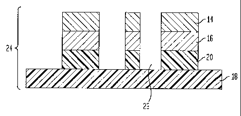
It will be appreciated that in areas where the transfer
adhesive 20 is applied, the metal 16 and coating 14 adhere to the
substrate l8, and are removed from the film 12. Tn the void
areas 23, the coating 14 and metal 16 remain adhered to the film
12, and are either discarded therewith or reused in a subsequent
process. In such a structure, the breakaway coating, metallized
area and selectively applied adhesive are in substantial
registration; i.e., aligned with one another so as to produce one
or more sharp or precise edges. Alternatively, substantially the
entire surface of the substrate 18 may be coated with the
transfer adhesive 20 such that it will be metallized in its
CA 02558461 2006-09-O1
WO 2005/091949 PCT/US2005/006902
entirety, rather than' selectively, if so desired. If the entire
surface is coated, there will be no void areas 23.
Fig. 4 depicts a schematic view of a preferred process for
selectively metallizing a substrate 18. In this preferred
5 process, the transfer film 10 is provided on a transfer film roll
11, with the coating 14 already cured and adhered to metal 16.
The transfer film 10 is unrolled from the transfer film roll 11
by a motor 32 in the direction indicated by arrow A.
Concurrently, the substrate 18 is unrolled from a substrate
10 roll 19 by a~motor 32 in the direction indicted by arrow B. As
the substrate 18 is unrolled, an electron beam curable transfer
adhesive 20 is, e.g., selectively applied by an applicator 21, to
form areas of curable transfer adhesive interposed with void
areas 23.
15 The transfer film 10 and the substrate 18 with selectively
applied transfer adhesive 20 may pass through a series of change
of direction pulleys or rollers 26, until they are brought
together in a pressure chamber or applicator 28. The pressure
chamber preferably applies a sufficient force to place the
20 transfer film 10 and the substrate 18 with selectively applied
transfer adhesive 20 into a position adjacent to, and in contact
with, each other, to form an intermediate product 22.
The intermediate product 22 is then exposed to EB radiation,
a . g. , by passing through an electron beam curing apparatus 30 to
cure the transfer adhesive 20. Typically, following the electron
beam curing apparatus 30, there may also be a mechanism to
disengage the film 12 from the remainder of the intermediate
product 22. In areas where transfer adhesive 20 has been applied
and cured, the film 12 is removed without the coating 14 adhering
to it. In the void areas 23, the film 12 is removed with the
coating 14 and the metal layer 12 still adhered. Thus, the
substrate 18 is selectively metallized. The substrate may then
be rolled into a finished product roll (not shown) or cut into
sheets (not shown) as desired.
In an alternative embodiment, the transfer adhesive 20 may
be applied directly to the metal layer 16 of the transfer film 10
CA 02558461 2006-09-O1
WO 2005/091949 PCT/US2005/006902
21
by the applicator 21 in order to form the intermediate product
22.
The coatings and adhesives utilized in preferred and
alternative embodiments of this invention include substantially
1000 active liquids (i.e., solvent or diluent is substantially
absent) such materials are typically referred to as 1000 solids
since, after curing, the amount of solid material is
substantially the same as the amount of liquid material at the
start. Preferably the transfer adhesive is EB curable and,
alternatively, the breakaway coating can also be EB curable. A
radiation curing process such as EB curing has the advantages of,
e.g., speed and the avoidance of volatile materials.
Specifically with regard to EB curable adhesives, the lack
of out-gassing during and following curing permits the use of
substrates which otherwise would be unavailable or more difficult
to process using non-EB curable adhesives. For example,
substrates used with non-EB curable adhesives are preferably
porous in order to permit out-gassing of solvents) and/or
diluent(s). With EB curable adhesives, nonporous substrates,
such as plastics, may be utilized.
With regard to coatings, the lack of out-gassing when EB is
used can reduce pitting of the coating upon curing. Such pitting
is undesirable as it creates small imperfections across the
surface and within the coating, potentially affecting the
smoothness, brightness and scuff resistance of the finished
product, among other characteristics. Furthermore, an
imperfection in an internal region of the coating may make it
susceptible to fracture in a place other than the one intended
when film is removed, thereby reducing the accuracy of the edges
in the metallized areas, particularly in a selectively metallized
structure.
Another advantage of EB curable adhesives over non-EB
curable adhesives is that non-EB curable adhesives typically must
be heated to be cured. Thermal curing typically requires
temperatures in the range of about 100 °F to about 500 °F;
alternatively, about 250 °F to about 350 °F. Tn contrast, EB
CA 02558461 2006-09-O1
WO 2005/091949 PCT/US2005/006902
22
curable adhesives may be cured at ambient temperature, typically
about 60 °F to about 90 °F; alternatively, about 65 °F to
about
80 °F, without the need to introduce a heat source. Because EB
curable adhesives do not require elevated temperatures to cure,
substrates that are susceptible damage due to heat, such as by
softening or even melting, may be utilized in the present process
where they may not have been suitable for use in processes
requiring elevated temperatures, e.g., the use of thin gauge
plastics, such as polyvinylchloride (PVC). The use of EB curing
also provides the opportunity for other cost savings, e.g.,
relating to faster and more uniform curing, lower coating
weights, etc.
Although EB curing may begin at ambient temperature, it is
understood that a moderate heat build-up may occur due to the
chemical reactions associated with curing and the energy input
associated with the EB equipment. This heat build-up is
typically on the order of a few degrees Fahrenheit, but may reach
ten or more degrees depending on the thickness of the adhesive
layer, the surface area being cured and the composition and
thickness of the overall layered structure. It is also to be
understood that the level of EB energy required for EB curing of
a particular adhesive composition may vary. Useful levels of
radiation doses are typically about 1 to about 6 megarads;
alternatively, about 3 to about 6 megarads may be utilized. The
dosing level typically depends on, and it is known how to adjust
for, the particular adhesive being utilized, as well as its
thickness and the surface area being covered, and the film and
metal deposition thicknesses.
Furthermore, it may be possible to apply EB curable coatings
and adhesives in thinner layers. In the present invention, the
thickness of a breakaway coating layer is typically about
0.5 microns to about 10 microns; preferably about 1.0 microns to
about 7 microns. Similarly, the thickness of the transfer
adhesive is typically about 2 microns to about 20 microns;
preferably about 4 microns to about 14 microns. Although
additional materials or layers are placed above the at least one
CA 02558461 2006-09-O1
WO 2005/091949 PCT/US2005/006902
23
adhesive layer in the finished product, its thin, uniform
cross-section contributes to the relatively smooth and/or desired
surface finish of the final product; e.g., where the surface
intentionally includes ridges, a holographic pattern, etc. It
will be appreciated that in this regard, as well as with respect
to other features of the invention, subsequently laid-down
surfaces develop attributes based in part on the surfaces upon
which they are applied. Thus, a thin, smooth adhesive layer
surface will contribute to the metal layer surface also being
smooth.
The thinness of the coating and adhesive layers can also
contribute to the ability of the finished product to flex. For
example, while cracking can occur on a score line in a paper
substrate metallized using non-EB curable adhesives, the use of
EB curable adhesives and, optionally, coatings, can help to avoid
such cracking Consequently, the finished product can be bent,
folded, or otherwise manipulated with only negligible degradation
in appearance, strength or other condition of the structure.
Another advantage of the process and product of the present
invention, including using EB curable adhesives and, optionally,
EB curable coatings, is that the finished product surface is hard
and scuff resistant. The level of hardness of the product on the
Sward Hardness scale is typically about 25 to about 75;
preferably, about 35 to about 65; for example, about 50.
Alternatively, it is about 50 to about 105; for example, about
100 on the Konig Hardness scale. Scuff resistances can be
measured using various test methods. For example, products of
the present invention tested for scuff resistance using the
Sutherland Rub Tester typically give results of about 50 to about
150 rubs face-to-face; for example about 100 rubs face-to-face
using a 4 1b. weight. Alternatively, tests using the Taber
Abraider Tester typically result in a weight loss of about O.lo
to about 2.0o, based on the total weight of the sample.
The ability to apply thin layers also provides benefits
relating to the application speed or operating speed of a
production line. In a typical process using non-EB curable
CA 02558461 2006-09-O1
WO 2005/091949 PCT/US2005/006902
24
adhesives and/or coatings utilizing substrates provided in rolls,
application speeds of up to about 600 feet per minute may be
realized. Because of the nature of the EB curable adhesives and
coatings, application speeds of about 800 to about 1500 feet per
minute may be achieved. Additionally, thinner layers can provide
acceptable overall diameters for standard size rolls of
intermediate and/or final products, e.g., nominally 72 inches, or
the use of larger diameter rolled products on existing equipment
with the concomitant advantage of fewer process interruptions.
Where substrates are metallized selectively using
conventional or prior art methods, rippling may occur in the roll
following the selective metallization process. Such rippling can
be caused by localized areas across the width .of the roll of
greater diameter adjacent to non-built-up areas, which have not
been metallized; thinner layers can mitigate such an effect.
Similar advantages may be achieved when the intermediate or
final products are stacked in sheets on a skid, rather than
rolled. In conventional processes, the thicker metallized areas
of the sheets can cause a stack to be non-uniform to the point of
instability, or require that the number of stacked sheets be
reduced. With sheets metallized in accordance with the present
invention, the additional thicknes s of the metallized portions is
sufficiently nominal compared to the non-metallized portions such
that the stack can remain generally uniform and stable, up to and
including, within commercial tolerances, heights utilized in the
industry for sheets or substrates prior to metallization.
The thinness and uniformity of the transfer adhesive layer,
particularly the preferred EB curable transfer adhesive, and the
use of a breakaway coating layer having the preferred properties
expressed hereinabove, permit selective metallization with
particularly straight, precise or sharp edges between metallized
and adjoining non-metallized areas, two adjoining metallized
areas with a non-metallized area between, or at the edges of a
substantially totally metallized construction or wherein total
transfer of metal has been carried out. In selective
metallization using non-EB curable adhesives, and. coatings that
CA 02558461 2006-09-O1
WO 2005/091949 PCT/US2005/006902
do not fracture to produce a fine line or precis a edge, but,
instead, elongate, the line or edge differentiating the
metallized areas from the non-metallized areas is not as sharp,
precise or distinct as in the present invention. For example,
5 applying the methods of the present invention, the edges of
adjoining selectively metallized areas can be produced wherein
the distance, in inches, between the adjoining a dges of such
areas typically differs by less than or equal to about ~0.010;
preferably less than or equal to about ~0.008; mo re preferably
10 less than or equal to about ~0.006; even more preferably less
than or equal to about ~0.004; most preferably less than or equal
to about ~0.002; for example, less than or equal to ~0.001. In a
substantially totally metallized structure, or where total
transfer of metal has taken place, these same values apply to the
15 straightness, sharpness or preciseness of an edge of the
metallized area. In other words, an edge produced using the
methods of the present invention will vary from an unwavering
line drawn along an edge and approximately mid-way through the
variations by the amounts expressed above. For applications
20 where high quality and precise or sharp, distinct lfines or areas
are of concern, EB curable adhesives and the break away coatings
of the present invention are particularly advantageo us. They are
also advantageous in processes where selectively met allized areas
are to be printed. In such instances, accurate registration of
25 the printing with the metallized portions is essential. With
distinct, precise or sharp lines between me tallized and
non-metallized areas, as well as metallized areas h awing sharply
or precisely defined boundaries, as defined above, such
registration can be more readily achieved. Additionally,
registration of the metal-containing portions of th a metal layer
and the breakaway coating are also improved significantly in the
present invention. Various methods are suitable for printing the
surface of the metallized structure, including where printed
matter is applied by a method selected from the group consisting
of offset, rotogravure, flexographic, letterpress and silk
screen.
CA 02558461 2006-09-O1
WO 2005/091949 PCT/US2005/006902
26
Furthermore with regard to printing, and wherein an EB
curable breakaway layer is used, the clarity and brightness of
the underlying metal layer is less susceptible to degradation by
the curing process and the thickness of the cured layer.
Additionally, in the absence of solvents or di1 uents, there are
fewer extraneous materials to interfere with the properties and
uniformity of the breakaway layer or to introduce irregularities
for the diffraction of light.
Other properties of the structures produce d by the methods
of the present invention have been measured and are indicative of
a preferred product. For example, where the surface of the
metallized structure is to be printed or glued, such as in
forming a container, the surface energy of a surface must be
suitable for the surface tension of liquids such as adhesives and
inks applied to the surface of the finished product; this is
particularly so at the exposed surface of the breakaway coating.
This characteristic is frequently referred to as the "dyne level"
of the surface, although the term used in ASTM D 2578, a test
method for measuring this characteristic, is "wetting tension."
The terms are used to represent relative receptivity of a film
surface to the addition of inks, coatings, and adhesives.
Wetting tension is described as the maximum liquid surface
tension that will spread, rather than bead up, on the film
surface. It is a measurable property that estimates the surface
energy of a film surface. ASTM D 2578 provides a method for
determining wetting tension by applying differen t test solutions
of increasing surface tension values until one is found that just
spreads or wets the film surface; values are expressed in
dynes/cm. The ASTM method is directed to polyethylene and
polypropylene films, but the same testing approach can be applied
to another film or coated film surface of interes t. For example,
FINAT FTM 15, an alternative, but similar test ing approach is
used for plastic films including polyethylene, polypropylene,
polyester and polyvinylchloride using test fluids suited to the
material under test. (Test methods ASTM D 2 578 and FTM 15
incorporated herein by reference; ASTM International, West
CA 02558461 2006-09-O1
WO 2005/091949 PCT/US2005/006902
27
Conshohocken, Pennsylvania, USA; and FINAT, The Hague, The
Netherlands) For purposes of the present invention, the dyne
level is typically in the range of about 32 to about 58 dynes/cm;
preferably about 34 to about 58 dynes/cm; more preferably ab out
36 to about 58 dynes/cm; most preferably about 36 to ab out
56 dynes/cm.
Finished product made in accordance with the present
invention and tested in an Atlas Fadeometer test typica 11y
exhibits acceptable levels of discoloration after about 40 to
about 60 hours; preferably, there is no discernible color change,
by eye, after 48 hours of exposure. Similarly, finished product
in accordance with the present invention tested in a
Weatherometer instrument according to standard test meth ods
appropriate for the use of the particular product, e.g., about 80
to about 100 hours, exhibits less than about 100 loss in
functionality of the relevant property. For example, properties
that may be considered relevant depending on the applicat ion
include gloss, adhesion, tensile strength, etc.
Also among the advantages of the present invention is the
adhesive bond strength achieved between the layers. The typi cal
failure mode observed is between the metal layer and the
underlying transfer adhesive layer; less commonly there can be
adhesive bond failure between the transfer adhesive and the
underlying substrate. Adhesive strength is measured using a h and
test and #600, 3M brand Scotch tape applied to the sample surf ace
and pulled away at a rate of approximately 1 ft./min. Where the
bond failure occurs between the metal and the transfer adhesive,
the material pulled away comprises the metal and breakaway lay ers
and, if used, a prime coat that would be applied between the
metal and breakaway layers. If the less common bond fail ure
occurs between the transfer adhesive and the substrate, the
material pulled away would also include the weight of the
transfer adhesive removed. Products of the present invent ion
typically exhibit the loss of less than about 2 wt.o of materi al;
preferably less than about 1 wt.o; more preferably less than
about 0.5 wt.o; for example, no loss. Such performance is
CA 02558461 2006-09-O1
WO 2005/091949 PCT/US2005/006902
28
particularly important as the layers tend not to delaminate, even
after repeated uses, including bending.
The stability of the finished structure, particularly its
ability to withstand delamination, and the thinness of the
finished product is especially advantageous when the technology
is used in the manufacture of credit cards. For purposes of the
present invention, the term "credit card" is used in the generic
sense and includes cards such as credit, debit, automatic teller
machine (ATM), identification, driver's license, security pass
cards, etc. Such cards are typically about 5.4 cm wide by about
8.6 cm long. Credit cards are typically held to a thickness of
about 30 mm or less to provide uniform operation in the various
slide mechanisms or card swipe devices used commercially, e.g.,
point-of-purchase devices, .ATM machines, etc. Conventional
metallization processes can add unwanted thickness to the credit
card, resulting in the need to use a thinner card-stock material
in order not to exceed the 30 mm industry maximum. Utilizing the
metallization method of the present invention, credit cards may
be formed using thicker stock materials than previously
achievable, thus adding to their strength and durability. In
addition, the development of high levels of adhesion between the
various layers of the overall structure as well as the ability to
use a thicker card-stock or substrate can also help to avoid
problems of curling due to the presence of layers having
dissimilar properties, e.g., thermal expansion rates.
Furthermore, the ability to produce a structure having high
levels of adhesion between the various layers, allows the
resulting product to be used in flexible packaging, where
delamination can be a significant problem. For example, one
potential use of a product in accordance with the present
invention is for toothpaste tubes, or containers. Presently,
toothpaste manufacturers market toothpaste in squeezable tubes
that generally are not metallized even though the boxes in which
they are packaged and sold are often metallized. The ability to
metallized the tube and box in the same manner may provide a
potential marketing advantage.
CA 02558461 2006-09-O1
WO 2005/091949 PCT/US2005/006902
29
The present invention is capable of producing the
above-described structures having higher gloss, better scuff
resistance and better adhesion that typical products of the prior
art. Generally the products are more esthetically pleasing and
display a preferred combination of properties compared to those
of the prior art, even though such prior art products may have
acceptable properties in one or another test.
The products of the present invention can be used in a wide
variety of applications. The structure can be used to
manufacture credit cards, bankcards, phone cards, licenses; or to
prepare articles of manufacture such as containers, wrapping
materials, displays, and signs. Containers can be made for use
with a wide variety of products, including foods, cosmetics,
drugs, smoking products, toys, electronics, kitchen utensils,
glassware, hardware, sporting goods, wearable items, and bottled
goods.
Example
A metallized structure of the present invention, made
according to a process, e.g., as illustrated in Fig. 2, is
manufactured in the following manner. A 0.5 mil clear polyester
transfer film is coated on one side by a gravure applicator using
a 180 quad engraved cylinder, with aromatic urethane acrylate
copolymer having a 70/30 weight ratio of urethane to acrylate
components (Grancoat~ 571) to a thickness of 3 microns. The
breakaway coating is oven dried at 250 °F in a gas fired, hot
air, low velocity oven. The dried coating layer has an
elongation at break when tested in tension of 0.7%. The coated
film is metallized on the coated side in a conventional vacuum
metallizer to an optical density of 2.0 on the coated side of the
film. The coated, metallized film is transported to an
Intraroto~ brand laminator equipped with an Energy Sciences
Incorporated EZ CureO brand electron beam (EB) unit. The coated
film is laminated on the coated metallized side to a 6 mil white
polystyrene plastic substrate, both film and substrate being in
web or roll form. An EB curable adhesive (Sun Chemical #7573) is
applied in the laminator to one surface of the polystyrene
CA 02558461 2006-09-O1
WO 2005/091949 PCT/US2005/006902
substrate by means of a flexographic printing head using a 200
analox roll (engraved cylinder) engraved to print 4 in. wide
stripes separated by 2 in. wide adhesive-free stripes . Both the
transfer coated polyester film and the polystyrene substrate are
5 40 inches wide overall, resulting in an overall product having
seven, 4 inch wide, coated strips and s ix, 2 inch wide, uncoated
strips . The EB adhesive is applied to provide a 4 micron thick
layer.
The EB cure cycle is set at 125K-V and 4.5 megarads. The
10 lamination process is conducted at 400 feet per minute, effecting
a cure time of 1.2 seconds. Within approximately 10 seconds
following EB cure, the polyester film is peeled way from the
composite, including the polystyrene substrate; the film comes
off clean, leaving the urethane acrylate coating and metal firmly
15 attached to only those 4 inch wide stripes to which the EB
adhesive has been applied. The meta11i2 ed areas of the polyester
carrier film corresponding to the 2 inch wide stripes to which no
EB adhesive is applied, remain attached to the removed polyester
film. In those areas where the metal layer is firmly attached to
20 the substrate, the configuration of the layers is: urethane
acrylate breakaway layer/ metal layer/ cured EB adhesive layer/
polystyrene substrate. The bond strength between the various
layers of the composite structure is capable of withstanding most
methods of commercial fabrication in various end uses. The
~5 finished metal-striped product is ready for use or further
conversion or fabrication in various end-uses, such as boxes,
displays, trading cards, etc.
Any range of numbers recited in the specification,
paragraphs hereinafter, or claims, describing various aspects of
30 the invention, such as that represent ing a particular set of
properties, units of measure, conditions, physical states or
percentages, is intended literally to incorporate expressly
herein by reference or otherwise, any rzumber falling within such
range, including any subset of numbers or ranges subsumed within
any range so recited. Additionally, the term "about" when used
as a modifier for, or in conjunction with, a variable, is
CA 02558461 2006-09-O1
WO 2005/091949 PCT/US2005/006902
31
intended to convey that the values and ranges disclosed herein
are flexible and that practice of the present invention by those
skilled in the art using, e.g., temperatures, concentrations,
amounts, contents, carbon numbers, properties such as elongation,
hardness, surface tension, viscosity, particle size, surface
area, solubility, etc., that are outside of the stated range or
different from a single value, will achieve the desired result,
namely, preparation of a metallized substrate having an improved
appearance in the metallized portions and comprising a layered
structure, methods of forming such a metallized substrate, and
metallized articles produced thereby.
Although the invention herein has been described with
reference to particular embodiments, it is to be understood that
these embodiments are merely illustrative of the principles and
applications of the present invention. It is therefore to be
understood that numerous modifications may be made to the
illustrative embodiments and that other arrangements may be
devised without departing from the spirit and scope of the
present invention as defined by the appended claims.