Note: Descriptions are shown in the official language in which they were submitted.
CA 02559146 2006-09-08
STA 242-Foreign BW/wa/XP
-1-
Functional layers for optical uses based on polythiophenes
The invention relates to transparent functional layers of electrically
conductive
polymers, their production and their use in optical constructions.
The optical properties of a body are determined by its shape and its material
properties. The relevant material properties for optical systems are the
refractive
index n and the absorption constant k (c~ Born, Max, Principles of Optics. 6th
ed.
1. Optics - Collected works ISBN 0-08-026482-4). The optical properties can be
modified by application of functional layers which are made of transparent
materials
and differ from the carrier in respect of n and/or k at least in parts of the
electromagnetic radiation spectrum. On the basis of these differences in n
and/or k,
reflection of radiation occurs at the interface between the functional layer
and
carrier. In this context, the Fresnel formulae (c~ Born, Max p. 38 et seq.)
describe
the distribution of reflected, absorbed and transmitted radiation.
Examples of such optical functional layers are: antireflection layers on
optical
elements, heat insulation layers on glazing panes cladding layers on glass
fibres,
interference layers on pearlescent pigments etc.
The economic importance of such optical functional layers is high, since the
optical
properties of an entire body can be changed relatively easily by these.
Possible transparent optical functional layers are materials which are
electrically
conductive, e.g. TCO layers (transparent conducting oxides), such as indium
tin
oxide (ITO) or antimony tin oxide (ATO), or thin metal layers or electrically
insulating layers, such as e.g. titanium dioxide, silicon dioxide, cryolite or
magnesium fluoride. Deposition of these inorganic layers is carned out by
sputtering, reactive sputtering or thermal vapour deposition in vacuo and is
therefore
involved and cost-intensive.
STA 242-Foreign
CA 02559146 2006-09-08
-2-
Inorganic optical functional layers have as disadvantages:
a) high process costs for the deposition, since vacuum installations are
necessary,
b) high material costs, in particular for ITO, ATO and metal layers,
c) brittleness of the layers, in particular the metal oxide layers,
d} the deposition and/or after-conditioning of the layers takes place at high
temperatures of T > 200 °C,
e) refractive index of the oxidic layers in the visual spectral range, i.e. in
the
wavelength range of 400 run < ~. < 760 nm, is high (n > 1.3) and can be
modified only with difficulty.
There has therefore continued to be a need for optical functional layers which
have
properties which are similar to or better than those of inorganic optical
functional
layers.
The obj ect of the present invention was therefore to produce optical
functional
layers which can replace the conventional expensive inorganic optical
functional
layers, but without having the disadvantages listed above.
It has been found, surprisingly, that a transparent layer which has a
refractive index
of n < 1.3 in parts of the visible spectral range and which meets the
requirements of
an optical functional layer can be produced by application of a solution
comprising
thiophene monomers and oxidizing agents.
The present invention therefore provides a transparent optical functional
layer,
characterized in that it has a refractive index of n < 1.3 in parts of the
visible spectral
range, in particular in a wavelength range comprising an interval of at least
50 nm,
preferably of at least 100 nm, and comprises at least one electrically
conductive
polymer which comprises at least one polythiophene with recurring units of the
general formula (I)
STA 242-Foreign
CA 02559146 2006-09-08
-3-
(1)
wherein
A represents an optionally substituted Cl-CS-alkylene radical, preferably an
optionally substituted CZ-C3-alkylene radical,
R represent a linear or branched, optionally substituted C~-C18-alkyl radical,
preferably linear or branched, optionally substituted Cl-Cla-alkyl radical, an
optionally substituted CS-C12-cycloalkyl radical, an optionally substituted C~-
C14-aryl radical, an optionally substituted C~-C18-aralkyl radical, an
optionally substituted C1-C4-hydroxyalkyl radical, preferably optionally
substituted Cl-CZ-hydroxyalkyl radical, or a hydroxyl radical,
x represents an integer from 0 to 8, preferably from 0 to 6, particularly
preferably 0 or 1, and
in the case where several radicals R are bonded to A, these can be identical
or
di fferent.
The general formula (I) is to be understood as meaning that x substituents R
can be
bonded to the alkylene radical A.
Further electrically conductive polymers which can also be employed in an
alternative embodiment according to the invention are optionally substituted
polypyrroles or optionally substituted polyanilines.
CA 02559146 2006-09-08
STA 242-Foreign
-4-
Polymers having a specific resistance of not more than 1O8S2~cm are to be
understood as electrically conductive polymers here.
In preferred embodiments, the polythiophenes with recurring units of the
general
formula (I) are those with recurring units of the general formula (Ia)
(Ia}
wherein
R and x have the abovementioned meaning.
In further preferred embodiments, the polythiophenes with recurnng units of
the
general formula (I) are those with recurring units of the general formula
(Iaa)
(Iaa) .
In the context of the invention, the prefix poly- is to be understood as
meaning that
more than one identical or different recurnng unit is contained in the polymer
or
polythiophene. The polythiophenes contain a total of y recurring units of the
general
formula (I), wherein y can be an integer from 2 to 2,000, preferably 2 to 100.
The
recurring units of the general formula (I) can in each case be identical or
different
within a polythiophene. Polythiophenes with in each case identical recurring
units
of the general formula (I) are preferred.
STA 242-Foreign
CA 02559146 2006-09-08
-5-
The polythiophenes preferably in each case carry H on the end groups.
In a particularly preferred embodiment, the polythiophene with recurring units
of the
general formula (I) is poly(3,4-ethylenedioxythiophene), i.e. a
homopolythiophene
S of recurring units of the formula (Iaa).
In a further preferred embodiment of the invention, the functional layer
comprises,
in addition to the polythiophene of the general formula (I), an anion of a
polymeric
carboxylic or sulfonic acid as a polymeric anion. This is particularly
preferably the
anion of polystyrenesulfonic acid.
In the context of the invention, CI-CS-alkylene radicals A are: in particular
methylene, ethylene, n-propylene, n-butylene or n-pentylene. In the context of
the
invention, C~-C1g-alkyl represents in particular linear or branched C~-C18-
alkyl
1 S radicals, such as, for example, methyl, ethyl, n- or iso-propyl, n-, iso-,
sec- or tert-
butyl, n-pentyl, 1-methylbutyl, 2-methylbutyl, 3-methylbutyl, 1-ethylpropyl,
1,1-
dimethylpropyl, 1,2-dimethylpropyl, 2,2-dimethylpropyl, n-hexyl, n-heptyl, n-
octyl,
2-ethylhexyl, n-nonyl, n-decyl, n-undecyl, n-dodecyl, n-tridecyl, n-
tetradecyl, n-
hexadecyl or n-octadecyl, CS-C12-cycloalkyl represents CS-C12-cycloalkyl
radicals,
such as, for example, cyclopentyl, cyclohexyl, cycloheptyl, cyclooctyl,
cyclononyl
or cyclodecyl, CS-C14-aryl represents CS-C14-aryl radicals, such as, for
example,
phenyl or naphthyl, and C~-C1g-aralkyl represents C~-C1g-aralkyl radicals,
such as,
for example, benzyl, o-, ,m-, p-tolyl, 2,3-, 2,4-, 2,S-, 2,6-, 3,4- or 3,S-
xylyl or
mesityl. The above list serves to explain the invention by way of example and
is not
2S to be regarded as conclusive.
Possible optional further substituents of the C1-CS-alkylene radicals A are
numerous
organic groups, for example alkyl, cycloalkyl, aryl, halogen, ether,
thioether,
disulfide, sulfoxide, sulfone, sulfonate, amino, aldehyde, keto, carboxylic
acid ester,
carboxylic acid, carbonate, carboxylate, cyano, alkylsilane and alkoxysilane
groups
as well as carboxamide groups.
STA 242-Foreign
CA 02559146 2006-09-08
-6-
The transparent optical functional layer according to the invention can be
applied to
any desired transparent substrate. Such a substrate can be, for example,
glass, extra
thin glass (flexible glass) or plastics.
Particularly suitable plastics are: polycarbonates, polyesters, such as e.g.
PET and
PEN (polyethylene terephthalate or polyethylene-naphthalene dicarboxylate),
copolycarbonates, polysulfone, polyether sulfone (PES), polyimide,
polyethylene,
polypropylene or cyclic polyolefins or cyclic olefin copolymers (COC),
hydrogenated styrene polymers or hydrogenated styrene copolymers.
Suitable polymer substrates can be, for example, films, such as polyester
films, PES
films from Sumitomo or polycarbonate films from Bayer AG (Makrofol~).
An adhesion promoter layer can be located between the substrate and the
functional
layer. Suitable adhesion promoters are, for example, silanes. Epoxysilanes,
such as,
for example, 3-glycidoxypropyltrimethoxysilane (Silquest~ A187, OSi
specialities),
are preferred. Other adhesion promoters with hydrophilic surface properties
can
also be used. Thus e.g. a thin layer of PEDT:PSS (poly3,4-
ethylenedioxythiophene:.
polystyrenesulfonic acid) is described as a suitable adhesion promoter for
PEDT
poly3,4-ethylenedioxythiophene (Hohnholz et al., Chem. Commun. 2001, 2444-
2445).
The polymeric optical functional layer according to the invention has the
following
advantages over the known inorganic optical functional layers described above:
It is
a) easy to apply from solution to any desired substrate, and expensive
deposition processes in vacuo are therefore eliminated,
b) not brittle and therefore also suitable for flexible substrates,
STA 242-Foreign
CA 02559146 2006-09-08
c) it has a low refractive index in the visible spectral range, which can
easily be
adapted by addition of other transparent polymers.
Production is expediently carried out such that the layer comprising at least
one
conductive polymer is produced from precursors for the preparation of
conductive
polymers corresponding to the formula (I) or aniline or pyrrole, optionally in
the
form of solutions, directly in situ on a suitable substrate by means of
chemical
oxidative polymerization in the presence of one or more oxidizing agents or by
means of electropolymerization. A layer comprising at least one polymeric
anion
and at least one polythiophene with recurring units of the general formula (I)
is
applied to this layer, in particular optionally after drying and washing, from
a
dispersion comprising at least one polymeric anion and at least one
polythiophene
with recurring units of the general formula (I).
The invention therefore also provides a process for the production of a
polymeric
optical functional layer according to the invention on a substrate,
characterized in
that the layer comprising at least one conductive polymer is produced by
applying to
the substrate precursors for the preparation of conductive polymers, such as
pyrrole
or aniline or, in particular, a thiophene corresponding to the general formula
(II)
A RX
H ~ ~ H (I~
S
in which A, R and x have the meaning given above for formula (I), optionally
in the
form of solutions, and chemical oxidative polymerization in the presence of
one or
more oxidizing agents or electrochemical polymerization is carried out to give
the
conductive polymers.
Possible suitable substrates are those already mentioned above. The substrate
can be
treated with an adhesion promoter before application of the layer comprising
at least
one conductive polymer. Such a treatment can be carried out, for example, by
spin-
STA 242-Foreign
CA 02559146 2006-09-08
_g_
coating, impregnation, pouring, dripping, spraying, atomizing, knife-coating,
brushing or printing, for example ink jet, screen, contact or tampon printing.
Precursors for the preparation of conductive polymers, also called precursors
in the
following, are understood as meaning corresponding monomers or derivatives
thereof. Mixtures of different precursors can also be used. Suitable monomeric
precursors are, for example, optionally substituted thiophenes, pyrroles or
anilines,
preferably optionally substituted thiophenes of the general formula (II)
/A
O ~O
/ (II)
S
wherein
A, R and x have the abovementioned meaning,
particularly preferably optionally substituted 3,4-alkylenedioxythiophenes of
the
general formula (IIa)
R
~-y x
O~O
(IIa).
S
In a preferred embodiment, 3,4-alkylenedioxythiophenes of the formula (IIaa)
O O
(IIaa)
S
are employed as monomeric precursors.
STA 242-Foreign
CA 02559146 2006-09-08
-9-
In the context of the invention, derivatives of these monomeric precursors are
understood as meaning, for example, dimers or trimers of these monomeric
precursors. Higher molecular weight derivatives, i.e. tetramers, pentamers
etc. of
the monomeric precursors are also possible as derivatives. The derivatives can
be
built up from both identical and different monomer units and can be employed
in the
pure form and in a mixture with one another and/or with the monomeric
precursors.
Oxidized or reduced forms of these precursors are also included in the term
"precursors" in the context of the invention as long as the same conductive
polymers
are formed during their polymerization as in the case of the precursors
described
above.
Possible substituents for the precursors, in particular for the thiophenes,
preferably
for the 3,4-alkylenedioxythiophenes, are the radicals mentioned for R for the
general
formula (1).
Processes for the preparation of the monomeric precursors for the preparation
of
conductive polymers and derivatives thereof are known to the expert and are
described, for example, in L. Groenendaal, F. Jonas, D. Freitag, H. Pielartzik
& J. R.
Reynolds, Adv. Mater. 12 (2000) 481 - 494 and literature cited therein.
The precursors can optionally be employed in the form of solutions. Suitable
solvents for the precursors which may be mentioned are, above all, the
following
organic solvents which are inert under the reaction conditions: aliphatic
alcohols,
such as methanol, ethanol, i-propanol and butanol; aliphatic ketones, such as
acetone
and methyl ethyl ketone; aliphatic carboxylic acid esters, such as ethyl
acetate and
butyl acetate; aromatic hydrocarbons, such as toluene and xylene; aliphatic
hydrocarbons, such as hexane, heptane and cyclohexane; chlorohydrocarbons,
such
as methylene chloride and dichloroethane; aliphatic nitrites, such as
acetonitrile;
aliphatic sulfoxides and sulfones, such as dimethylsulfoxide and sulfolane;
aliphatic
carboxylic acid amides, such as methylacetamide, dimethylacetamide and
dimethylformamide; and aliphatic and araliphatic ethers, such as diethyl ether
and
CA 02559146 2006-09-08
STA 242-Foreign
-10-
anisole. Water or a mixture of water with the abovementioned organic solvents
can
furthermore also be used as the solvent.
Further components, such as one or more organic binders which are soluble in
organic solvents, such as polyvinyl acetate, polycarbonate, polyvinylbutyral,
polyacrylic acid esters, polymethacrylic acid esters, polystyrene,
polyacrylonitrile,
polyvinyl chloride, polybutadiene, polyisoprene, polyethers, polyesters,
silicones
and styrene/acrylic acid ester, vinyl acetate/acrylic acid ester and
ethylene/vinyl
acetate copolymers, or water-soluble binders, such as polyvinyl alcohols,
crosslinking agents, such as polyurethanes or polyurethane dispersions,
polyacrylates, polyolefm dispersions, epoxysilanes, such as 3-
glycidoxypropyltrialkoxysilane, and/or additives, such as e.g. imidazole or
surface-
active substances, can moreover be added to the solutions. Alkoxysilane
hydrolysates, e.g. based on tetraethoxysilane, can furthermore be added to
increase
the scratch resistance in coatings or to increase the refractive index of the
in situ
layer in a controlled manner.
In the case where the precursors undergo chemical oxidative polymerization to
give
the conductive polymers, the presence of one or more oxidizing agents is
necessary.
Oxidizing agents which can be used are all the metal salts known to the expert
which
are suitable for oxidative polymerization of thiophenes, anilines or pyrroles.
Suitable metal salts are metal salts of main group or sub-group metals, the
latter also
being called transition metal salts in the following, of the periodic table of
elements.
Suitable transition metal salts are, in particular, salts of an inorganic or
organic acid
or inorganic acid containing organic radicals with transition metals, e.g.
with
iron(III), copper(II), chromium(VI), cerium(IV), manganese(IV), manganese(VII)
and ruthenium(III).
STA 242-Foreign
CA 02559146 2006-09-08
-11-
Preferred transition metal salts are those of iron(III). Iron(III) salts are
often
inexpensive and easily obtainable and can be handled easily, such as e.g. the
iron(III) salts of inorganic acids, such as, for example, iron(III) halides
(e.g. FeCl3)
or iron(III) salts of other inorganic acids, such as Fe(C104)3 or Fez(S04)3,
and the
iron(III) salts of organic acids and inorganic acids containing organic
radicals.
Examples which may be mentioned of iron(III) salts of inorganic acids
containing
organic radicals are the iron(III) salts of the sulfuric acid monoesters of C~-
Czo-
alkanols, e.g. the iron(III) salts of lauryl sulfate.
Particularly preferred transition metal salts are those of an organic acid, in
particular
iron(III) salts of organic acids.
Examples of iron(III) salts which may be mentioned are: the iron(III) salts of
C1-Czo-
alkanesulfonic acids, such as methane-, ethane-, propane- or butanesulfonic
acid or
higher sulfonic acids, such as dodecanesulfonic acid, of aliphatic
perfluorosulfonic
acids, such as trifluoromethanesulfonic acid, perfluorobutanesulfonic acid or
perfluorooctanesulfonic acid, of aliphatic C~-Czo-carboxylic acids, such as 2-
ethylhexylcarboxylic acid, of aliphatic perfluorocarboxylic acids, such as
trifluoroacetic acid or perfluorooctanoic acid, and of aromatic sulfonic acids
which
are optionally substituted by C~-Czo-alkyl groups, such as benzenesulfonic
acid, o-
toluenesulfonic acid, p-toluenesulfonic acid or dodecylbenzenesulfonic acid,
and of
cycloalkanesulfonic acids, such as camphorsulfonic acid.
Any desired mixtures of these abovementioned iron(III) salts of organic acids
can
also be employed.
The use of the iron(III) salts of organic acids and inorganic acids containing
organic
radicals has the great advantage that they do not have a corrosive action.
STA 242-Foreign
CA 02559146 2006-09-08
-12-
Iron(III) p-toluenesulfonate, iron(III) o-toluenesulfonate or a mixture of
iron(III) p-
toluenesulfonate and iron(III) o-toluenesulfonate are very particularly
preferred as
metal salts.
In preferred embodiments, the metal salts have been treated with an ion
exchanger,
preferably a basic anion exchanger, before their use. Examples of suitable ion
exchangers are macroporous styrene and divinylbenzene polymers which have been
functionalized with tertiary amines, such as are marketed e.g. under the trade
name
Lewatit~ by Bayer AG, Leverkusen.
Oxidizing agents which are furthermore suitable are peroxo compounds, such as
peroxodisulfates (persulfates), in particular ammonium and alkali metal
peroxodisulfates, such as sodium and potassium peroxodisulfate, or alkali
metal
perborates - optionally in the presence of catalytic amounts of metal ions,
such as
iron, cobalt, nickel, molybdenum or vanadium ions - and transition metal
oxides,
such as e.g. pyrolusite (manganese(IV) oxide) or cerium(IV) oxide.
For the oxidative polymerization of the thiophenes of the formula (II), in
theory 2.25
equivalents of oxidizing agent are required per mol of thiophene (see e.g. J.
Polym.
Sc. Part A Polymer Chemistry vol. 26, p. 1287 (1988)). However, lower or
higher
numbers of equivalents of oxidizing agent can also be employed. In the context
of
the invention, preferably one equivalent or more, particularly preferably 2
equivalents or more of oxidizing agent are employed per mol of thiophene.
The anions of the oxidizing agent used can preferably serve as counter-ions,
so that
in the case of chemically oxidative polymerization an addition of additional
counter-
ions is not absolutely necessary.
The oxidizing agents can be applied to the substrate together with or
separately from
the precursors - optionally in the form of solutions. If the precursors,
oxidizing
agents and optionally counter-ions are applied separately, the substrate is
preferably
STA 242-Foreign
CA 02559146 2006-09-08
-13-
first coated with the solution of the oxidizing agent and optionally the
counter-ions
and then with the solution of the precursors. In the case of the preferred
joint
application of thiophenes, oxidizing agent and optionally counter-ions, the
oxide
layer of the anode body is coated with only one solution, namely a solution
containing thiophenes, oxidizing agent and optionally counter-ions. Possible
solvents in all cases are those solvents described above as suitable for the
precursors.
The solutions can moreover comprise as further components (binders,
crosslinking
agents etc.) the components already described above for the solutions of the
precursors.
The solutions to be applied to the substrate preferably comprise 1 to 30 wt.%
of the
precursors, preferably of the thiophenes of the general formula (II), and
optionally 0
to 50 wt.% of binders, crosslinking agents and/or additives, both percentages
by
weight being based on the total weight of the solution.
The solutions are applied by known processes, e.g. by spin-coating,
impregnation,
pouring, dripping, spraying, atomizing, knife-coating, brushing or printing,
for
example ink jet, screen or tampon printing.
The removal of any solvent present after application of the solutions can take
place
by simple evaporation at room temperature. However, to achieve higher
processing
speeds it is more advantageous to remove the solvents at elevated
temperatures, e.g.
at temperatures from 20 to 300 °C, preferably 40 to 250 °C. An
after-treatment with
heat can be combined directly with the removal of the solvent or can also be
carried
out at a separate time from the production of the coating. The solvents can be
removed before, during or after the polymerization.
The duration of the heat treatment can be 5 seconds to several hours,
depending on
the nature of the polymer used for the coating. Temperature profiles with
different
temperatures and dwell times can also be employed for the heat treatment.
STA 242-Foreign
CA 02559146 2006-09-08
-14-
The heat treatment can be carried out e.g. by moving the coated substrates
through a
heating chamber, which is at the desired temperature, at a speed such that the
desired
dwell time at the chosen temperature is achieved, or by bringing them into
contact
with a hot-plate, which is at the desired temperature, for the desired dwell
time. The
heat treatment can furthermore be carried out, for example, in a heating oven
or
several heating ovens each with different temperatures.
After removal of the solvents (drying) and if appropriate after the after-
treatment
with heat, it may be advantageous to wash the excess oxidizing agent and
residual
salts out of the layer with a suitable solvent, preferably water or alcohols.
Residual
salts here are to be understood as meaning the salts of the reduced form of
the
oxidizing agent and any further salts present.
The electrochemical polymerization can be carried out by processes known to
the
expert.
If the thiophenes of the general formula (II) are liquid, the
electropolymerization can
be carried out in the presence or absence of solvents which are inert under
the
electropolymerization conditions; the electropolymerization of solid
thiophenes of
the general formula (II) is carned out in the presence of solvents which are
inert
under the electrochemical polymerization conditions. In certain cases it may
be
advantageous to employ solvent mixtures and/or to add solubilizing agents
(detergents) to the solvents.
Examples which may be mentioned of solvents which are inert under the
electropolymerization conditions are: water; alcohols, such as methanol and
ethanol;
ketones, such as acetophenone; halogenated hydrocarbons, such as methylene
chloride, chloroform, carbon tetrachloride and fluorohydrocarbons; esters such
as
ethyl acetate and butyl acetate; carbonic acid esters, such as propylene
carbonate;
aromatic hydrocarbons, such as benzene, toluene and xylene; aliphatic
STA 242-Foreign
CA 02559146 2006-09-08
-15-
hydrocarbons, such as pentane, hexane, heptane and cyclohexane; nitriles, such
as
acetonitrile and benzonitrile; sulfoxides, such as dimethylsulfoxide;
sulfones, such
as dimethyl sulfone, phenyl methyl sulfone and sulfolane; liquid aliphatic
amides,
such as methylacetamide, dimethylacetamide, dimethylformamide, pyrrolidone, N-
methylpyrrolidone and N-methylcaprolactam; aliphatic and mixed aliphatic-
aromatic ethers, such as diethyl ether and anisole; liquid ureas, such as
tetramethylurea; or N,N-dimethyl-imidazolidinone.
For the electropolymerization, electrolyte additions are added to the
thiophenes of
the general formula (II) or solutions thereof. Free acids or conventional
conductive
salts which have a certain solubility in the solvents used are preferably used
as
electrolyte additions. Electrolyte additions which have proved suitable are
e.g.: free
acids, such as p-toluenesulfonic acid and methanesulfonic acid, and
furthermore
salts with alkanesulfonate, aromatic sulfonate, tetrafluoroborate,
hexafluorophosphate, perchlorate, hexafluoroantimonate, hexafluoroarsenate and
hexachloroantimonate anions and alkali metal, alkaline earth metal or
optionally
alkylated ammonium, phosphonium, sulfonium and oxonium canons.
The concentrations of the monomeric thiophenes of the general formula (II) can
be
between 0.01 and 100 wt.% (100 wt.% only in the case of liquid thiophene); the
concentrations are preferably 0.1 to 20 wt.%, based on the total weight of the
solution.
The electropolymerization can be carried out discontinuously or continuously.
The current density for the electropolymerization can vary within wide limits;
a
current density of 0.0001 to 100 mA/cmZ, preferably 0.01 to 40 mA/cm2 is
conventionally used. A voltage of about 0.1 to 50 V is established at this
current
density.
STA 242-Foreign
CA 02559146 2006-09-08
-16-
Suitable counter-ions are those already mentioned above. In the
electrochemical
polymerization, these counter-ions can optionally be added to the solution or
the
thiophenes as electrolyte additions or conductive salts.
The electrochemical oxidative polymerization of the thiophenes of the general
formula (II) can be carried out at a temperature from -78 °C up to the
boiling point
of the solvent optionally employed. The electrochemical polymerization is
preferably carried out at a temperature from -78 °C to 250 °C,
particularly preferably
-20 °C to 60 °C.
The reaction times are preferably 1 minute to 24 hours, depending on the
thiophene
used, the electrolytes used, the temperature chosen and the current density
applied.
In the electrochemical polymerization, the substrate, which as a rule is not
1 S conductive, is first coated with a thin transparent layer of a conductive
polymer, as
described in Groenendaal et al. Adv. Mat. 2003, 15, 855. The substrate coated
with
a conductive coating in this way, with a surface resistance of > 104 S2/sq,
takes over
the function of the Pt electrode during the subsequent electropolymerization.
The
layer comprising the conductive polymer grows on top when a voltage is
applied.
Since the conductive polymers) in the layer comprising at least one conductive
polymer are produced directly by polymerization of precursors in situ on the
substrate, this layer is also called the "in situ layer" in the following. The
concept of
in situ deposition of a conductive polymer from a polymerizable solution of
monomer and oxidizing agent is generally known in technical circles.
A polymeric optical functional layer can be produced by the process according
to the
invention without involved and expensive CVD, vapour deposition or sputtering
processes being necessary. Inter alia, use of the process according to the
invention
over a large area is also rendered possible by this means. Furthermore, the in
situ
layer can be applied at low temperatures, preferably room temperature. The
process
STA 242-Foreign
CA 02559146 2006-09-08
- 17-
according to the invention is thus also suitable for application to polymeric,
flexible
substrates which as a rule tolerate only low temperature processes and do not
withstand the temperatures of thermal CVD or of reactive sputtering during
deposition.
The optical functional layer according to the invention preferably has a
transmission
of Y > 25 %. The transmission is determined by the measurement methods, such
as
is described in the specification ASTM D 1003-00. The transmission is then
calculated in accordance with ASTM E 308 (light type C, 2*observers).
The polymeric layers according to the invention are outstandingly suitable as
optical
functional layers, such as antireflection layers on optical elements and
glazing panes,
heat insulation layers on glazing panes, cladding layers on glass fibres and
interference layers on pearlescent pigments.
The preferred functional layer - comprising a polydioxythiophene - is
distinguished
by the particular course of its dispersion and absorption curve and is
therefore
particularly suitable as an optical functional layer. The dispersion curve
describes
. the spectral dependence of the refraction index; the absorption curve
describes the
spectral dependence of the absorption constant.
Polymeric optical functional layers based on the layer according to the
invention are
of advantage in the following uses:
1.) Antireflection layers on surfaces (cf. Born, Max p. S 1 et seq.)
By application of a transparent functional layer, antireflection layers can be
generated by depositing these layers in defined thicknesses. If the optical
path length of this layer is equal to one quarter of the wavelength, i.e. nL*d
=
7~,/4, destructive interference of the two partial beams reflected on the
upper
and lower side of the layer occurs. If the reflected partial beams have the
STA 242-Foreign
CA 02559146 2006-09-08
-18-
same intensity, in total no light is reflected. So that the reflected partial
beams have the same intensity, the refractive index of the antireflection
layer
should be equal to the geometric mean of the refractive indices of air and the
support, i.e. nL = ~(nA*ns) (cf. Born, Max p. 64 et seq.). Since nA = 1 and ns
= 1.5 for glass, the refractive index of the antireflection layer applied
should
ideally be nL = 1.22.
Transparent inorganic materials, such as e.g. titanium dioxide, silicon
dioxide, cryolite or magnesium fluoride, are conventionally deposited as a
thin film as antireflection layers. All these inorganic layers have a
refractive
index which is significantly above the desired geometric refractive index of n
= 1.22. For example, the refractive index of cryolite is n = 1.35, or that of
MgF2 is n = 1.38. Transparent solids with a low refractive index of n < 1.3
have not hitherto been used as antireflection layers.
Because the refractive index is too high, antireflection layers are therefore
deposited e.g. on glass as multilayer systems. In this procedure, thin
inorganic layers with a different refractive index are deposited on one
another in alternating sequence, as described e.g. in US-A 4726654.
The abovementioned inorganic antireflection layers are deposited by known
thin layer deposition processes, such as thermal vapour deposition,
sputtering, CVD (Chemical Vapor Deposition) etc. These processes are
involved and therefore expensive, since all require a vacuum and the
deposition rates are slow.
It has been found, surprisingly, that by application of a layer comprising in
situ PEDT to PET film or quartz glass, the reflection of a support in the
visible spectral range can be significantly reduced. Since the layer
comprising PEDT has a very low refractive index of n = 0.8 - 1.3 in the
visible spectral range with a simultaneously high transparency, a thin layer
of
STA 242-Foreign
CA 02559146 2006-09-08
-19-
this material can be used as an antireflection layer. The optical constants of
a
thin layer are determined by two known methods of thin layer optics by
iterative fitting of the reflection and transmission curves of two layers of
different layer thickness. In the first method, n and k are calculated
iteratively with the aid of the Fresnel formulae. In the second method the
ETA-RT apparatus of Steag EtaOptik GmbH, Heinsberg, Germany and the
software integrated therein for the determination of the values of n and k are
used. Both methods produce similar results.
The low refractive index in wide parts of the visible spectral region of the
in
situ layer according to the invention of n < 1.3 has the following advantages:
a) The refractive index of the layer according to the invention can be
adjusted - as has surprisingly been found - in a controlled manner
such that this corresponds to the geometric mean of the refractive
indices of air nA and the substrate ns. High antireflection effects can
already be achieved with an individual layer in this way. The
adjustment is made by mixing a certain amount of a polymer with a
refractive index of nlsP < nP which is soluble in the in situ PEDT
solution with the in situ PEDT solution. The refractive index of the
layer nL can then be easily calculated from:
nL - nISP * plSP + nP * pP
where nlsP and nP are the refractive indices of the pure in situ PEDT
and the pure polymer layer respectively and plsP and pP are the
corresponding volume contents. Suitable polymers with nlsP < nP and
an adequate solubility in an in situ PEDT solution are described
above in more detail.
STA 242-Foreign
CA 02559146 2006-09-08
-20-
b) The layer comprising in situ PEDT can be applied very much more
easily to the desired support from solution by employing inexpensive
deposition processes - as described above in more detail.
S 2.) Coating layer on effect pigments
Coated mica platelets are used as pearlescent effect pigments for colouring
lacquers (cf. Iridin~ pigments, Merck, Darmstadt). The pearlescent effect is
produced by a thin layer which is precipitated on to the mica carrier. As
described above under 1.), an interference phenomenon also occurs here.
Certain regions of the visible spectral range are preferentially reflected or
absorbed, and as a result the particular colour impression is formed
These pigments are conventionally coated with inorganic layers, such as e.g.
Ti02 or Si02. Because of the low refractive index and its unique spectral
course, a thin layer of PEDT enables a coloured pigment with new improved
properties to be prepared.
3.) Infrared reflection layer on surfaces
The heating up of closed rooms behind panes of glass through which
sunlight can penetrate can be reduced by providing the panes of glass with
an infrared-reflecting protective layer (IR reflection layer). Since this
layer
at the same time should be transparent in the visible spectral range,
inorganic
coatings, such as indium tin oxide (ITO) or antimony tin oxide are
conventionally used as an IR reflection layer for panes of glass (cf. K
glass).
It has been found, surprisingly, that by application of a layer comprising in
situ PEDT to PET film or quartz glass, the IR reflection of the carrier in the
wavelength range of the thermal radiation of the sun, i.e. in the range of 7~
>
STA 242-Foreign
CA 02559146 2006-09-08
-21 -
750 nm, can be increased significantly. As a result, less IR light is allowed
through and the warming up of the room behind the pane can be reduced.
4.) Wave conductor, cladding of glass fibres
S
Optical glass fibres are coated with a cladding layer (c~ Bergmann Schaefer,
volume 3 Optik, p. 449 et seq., 9th edition) to protect the sensitive surface
of
the glass fibres against scratching. For this, in the case of glass fibres the
outer region of the glass fibre is suitably doped, i.e. provided with
impurities
in a controlled manner, in order to lower the refractive index in the relevant
spectral transition range relative to the inside of the fibre. The signal
remains, due to this refractive index gradient and the associated total
reflection, inside the fibre and disturbances on the surface, such as e.g.
scratches, no longer act as scattering centres.
The process described above of doping glass in the outer region has the
disadvantage that this process can be realized only during production of the
glass fibre. The region of total reflection is thereby limited to a relatively
narrow wavelength range.
Because of the low refractive index of in situ PEDT, this material is also
suitable as a cladding layer for glass fibres, with the advantage that this
layer
can also still be applied subsequently and easily to the glass or polymer
light
conductor fibres and total reflection is retained in wide regions in the
visible
and IR range.
The effect found is unexpected, since no polymers which can be applied from
solution and have a refractive index of n < 1.3 in the visible spectral range,
or high
reflection properties for wavelengths in the near infrared were known
hitherto.
STA 242-Foreign
CA 02559146 2006-09-08
-22-
The invention is explained in the following by way of example by means of the
figures.
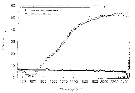
The figures show:
Fig. 1 A graph which shows the reflection of an in situ PEDT layer on a quartz
substrate as a function of the wavelength in comparison with a layer merely
of quartz,
Fig.2 a graph similar to fig. 1 with a layer comprising poly-3,4-ethylene-
dioxythiophene and polysulfonic acid,
Fig. 3 a graph similar to fig. 1 for the' measurement on in situ coated and
non-
coated PET film,
Fig. 4 a further graph similar to fig. 3.
STA 242-Forei~,n
CA 02559146 2006-09-08
-23-
Examples
Example 1
In situ PEDT layers on quartz~l, ass:
Epoxysilane (Silquest~ A187, manufacturer OSi specialities), diluted with
20 parts of 2-propanol, is spun-coated on to cleaned quartz substrates with a
spin-coater and then dried at 50 °C for 5 min in air. The layer
thicknesses
are less than 20 nm. A solution comprising 3,4-ethylenedioxythiophene
(Baytron~ M), a 6 % strength solution of iron(III) (tosylate)3 in butanol
(Baytron~ CB 40, manufacturer H.C. Starck GmbH), and imidazole in a wt.
ratio of 1 : 20 : 0.5 is prepared and filtered (Millipore HV, 0.45 ~.m).
Thereafter, the solution is spun-coated with a spin-coater at 1,000 rpm on to
the quartz substrates coated with epoxysilane. The layer is subsequently
dried at room temperature (RT, 23 °C) and then rinsed thoroughly with
dist.
water in order to remove the iron salts. After drying of the layers, the layer
thickness is approx. 155 nm. The layers have smooth surfaces with a surface
roughness Sr of < 5 nm. The conductivity of the layers is 550 S/cm. The
transparency of the layers is high. Thus, the transparency Y of a layer
200 nm thick on the glass substrate is > 50 %.
The reflection spectra of the layers on quartz are recorded with a
spectrophotometer (Perkin-Elmer Lamda 900, equipped with an Ulbricht
globe) in accordance with DIN 5036. Figure 1 shows the reflection spectra.
It can be clearly seen that the reflection in wide parts of the visible
spectral
range is lower than that of non-coated quartz glass. At 550 nm in particular,
the maximum of the sensitivity curve of the eye, the reflection of the 155 nm
thick in situ PEDT layer an quartz is only 1.4 %, compared with 6.8 % for
non-coated quartz. The in situ PEDT layer therefore leads to antireflection
of the quartz substrate in the visible spectral range.
STA 242-Foreign
CA 02559146 2006-09-08
-24-
At a wavelength of 2,000 nm the reflection in the in situ PEDT layer on
quartz is 51.5 %, compared with 6.1 % on non-coated quartz. The in situ
PEDT layer thus reflects in the near IR range to a greater degree than the
S quartz substrate.
Example 2
Baytron P~ AI4071 layers onguartz l~ ass:
A mixture of poly(3,4-ethylenedioxythiophene) and polystyrenesulfonic acid
(1 : 2.5 parts by wt.) Baytron P° AI4071 is spun-coated at 1,000 rpm on
to
cleaned quartz substrates. The layer is then dried at 200 °C. After
drying of
the layers, the layer thickness is approx. 180 nm. The layers have smooth
1 S surfaces with a surface roughness Sr of < 5 nm. The conductivity of the
layers is 0.1 S/cm.
The reflection spectra are shown in figure 2.
At a wavelength of 700 nm the reflection of the Baytron P~ AI4071 layer on
quartz is 4.8 %, compared with 6.7 % in the case of non-coated quartz. The
Baytron P~ AI4071 layer therefore leads to an antireflection of the quartz
substrate in the visible spectral range.
At a wavelength of 2,000 nm the reflection of the Baytron P~ AI4071 layer
on quartz is 16.2 %, compared with 6.1 % in the case of non-coated quartz.
The Baytron P~ AI4071 layer thus reflects in the near IR range to a greater
degree than the quartz substrate.
STA 242-Foreign
CA 02559146 2006-09-08
- 25 -
Example 3
As in example 1, an in situ PEDT layer is deposited on quartz glass and the
reflection and transmission spectra are measured, with the difference that the
S speed of revolution is 2,000 rpm and the layer thickness is 95 nm.
Example 4
As in example 2, a Baytron P° AI4071 layer is deposited on quartz
glass and
the reflection and transmission spectra are measured, with the difference that
the speed of revolution is 2,000 rpm and the layer thickness is 100 nm.
Example 5
With the layers produced according to example 1 and 3 and example 2 and
4, the dispersion and absorption curves of the in situ PEDT layer and of the
Baytron P° AI4071 layer on quartz glass are determined. The
determination
is carried out with two different methods, which produce results which are in
agreement. Method 1 is a computer program which is based on the Fresnel
formulae and fits the n and k iteratively until the calculated R and T courses
correspond to those measured on the two specimens of different layer
thickness. Method 2 uses the ETA-RT apparatus of Steag EtaOptik, with
which n and k can be determined from R and T spectra of thin layers on a
substrate. The two methods produce a similar result, which is summarized
in table 1.
It follows from table 1 that an in situ PEDT layer has a refractive index of
n < 1.3 in wide parts of the visible spectral ranges, whereas a Baytron
P°
AI4701 layer - which, with the PSS, comprises an electrically non-
conductive component - has a higher refractive index.
STA 242-Foreign
CA 02559146 2006-09-08
-26-
Table 1: Dispersion and absorption curves of in situ PEDT and Baytron P AI4071
A,I4071 in situ PEDT
?~ (nm) n k n k
350 1.515 0.016 1.4825 0.0485
400 1.495 0.019 1.3945 0.069
450 1.477 0.023 1.316 0.1005
500 1.460 0.028 1.245 0.1435
550 1.446 0.035 1.182 0.1975
600 1.432 0.044 1.1255 0.262
650 1.420 0.053 1.081 0.3385
700 1.410 0.064 1.044 0.425
750 1.400 0.076 1.014 0.523
800 1.392 0.089 0.9915 0.632
850 1.385 0.105
Example 6
As in example 1, an in situ PEDT layer is deposited and measured, with the
difference that the solution comprising Baytron~ M, Baytrori CB 40 and
DMSO in a wt. ratio of 1 : 20 : 1.25 is prepared and this solution is applied
to
PET film with a doctor blade. The doctor blade used leads to a wet layer
thickness of d = 12 pm.
The reflection spectra of the film coated in this way are shown in figure 3 of
the appendix in comparison with non-coated PET film.
The reflection is significantly lower in the visible spectral range with the
coating than without a coating. Thus, the reflection at 490 nm R = 3.62
with the coating, compared with R = 9.9 % without a coating. In the near IR,
on the other hand, the reflection is higher with the coating, thus the
reflection
STA 242-Foreign
CA 02559146 2006-09-08
-27-
at 2,400 nm R = 46.9 % with the coating, compared with R = 6.5 % without
a coating.
This shows that the layer according to the invention leads to a reduction of
the reflection in the visible spectral range and to an increase in the
reflection
in the near IR.
Example 7
As in example 1, an in situ PEDT layer is deposited and measured, with the
difference that the solution comprising Baytron° M, Baytron~ CB 40,
DMSO and a polyurethane-based crosslinking agent Desmotherm~ 2170
(manufacturer Bayer AG) in a wt. ratio of 1 : 20 : 1.25 : 0.5 is prepared and
this solution is applied to PET film with a doctor blade. The doctor blade
used leads to a wet layer thickness of d = 12 Vim.
The reflection spectra of the film coated in this way are shown in figure 4 of
the appendix in comparison with non-coated PET film.
The reflection is significantly lower in the visible spectral range with the
coating than without a coating. Thus, the reflection at 650 nm R = 2.60
with the coating, compared with R = 9.5 % without a coating. In the near IR,
on the other hand, the reflection is higher with the coating, thus the
reflection
at 2,400 nm wavelength R = 41.5 % with the coating, compared with
R = 6.5 % without a coating.
This shows that the layer according to the invention leads to a reduction of
the reflection in the visible spectral range and to an increase in the
reflection
in the near IR. This example furthermore shows in particular, in comparison
with example 6, that the spectral course of the reflection can be changed by
STA 242-Foreign
CA 02559146 2006-09-08
- 28 -
the addition of the crosslinking agent Desmotherm 2170 under the same
deposition conditions.