Note: Descriptions are shown in the official language in which they were submitted.
CA 02559195 2006-09-08
-1-
Test element analysis system with contact surfaces coated with hard material
Field of the invention
The invention concerns a test element analytical system for the analytical
examination of a sample and in particular a body fluid of humans or animals.
The
system comprises at least two components i.e. a test element which has a
measuring
zone into which the sample to be examined is moved in order to carry out an
analysis
in order to measure a measurable variable that is characteristic for the
analysis and an
evaluation device with a test element holder in order to position the test
element in a
measuring position in order to carry out the measurement and a measuring
device
for measuring the characteristic measurable variable.
State of the art
Test element analytical systems are commonly used especially in medical
diagnostics
for analysing body fluids such as blood or urine. The sample to be examined is
firstly
applied to a test element. Here the process steps that are required to detect
the analyte
which are usually chemical, biochemical, biological or immunological detection
reactions or physical interactions take place which result in a characteristic
and
measurable change of the test element especially in the area of the measuring
zone. In
order to determine this characteristic change the test element is inserted
into an
evaluation device which determines the characteristic change of the test
element and
provides it in the form of a measured value for display or further processing.
Test elements are often designed as test strips which are essentially composed
of an
elongate support layer, usually made of a plastic material, and a measuring
zone with
a detection layer containing detection reagents and, if necessary, other
auxiliary layers
such as filtration layers. The test elements of the present invention
additionally
contain contact areas which can be used to make an electrical contact between
the
test element and the evaluation device. In the case of electrochemical assay
methods
conductor paths and electrodes are mounted on the test element. Even test
elements
which do not use methods of electrochemical analysis can have electrically
CA 02559195 2006-09-08
-2-
conducting contact areas for example in order to transfer calibration data or
batch
information that are stored on the test element to the evaluation instrument.
The accompanying evaluation devices have test element holders with special
contact
elements which make an electrically conducting contact between the test
element and
the measuring and evaluation electronics of the evaluation instrument. These
contact
elements are usually in the form of electrical plug connections with metallic
spring
elements which are often provided with a noble metal surface usually of gold
or
platinum. The test strips are inserted into the test element holder for the
measurement during which the contact areas of the contact elements are moved
across the electrodes of the test elements. In an end position the contact
area of the
contact elements of the evaluation instrument are then in contact with the
contact
area of the test element. An electrically conducting connection is made
between the
test element and evaluation instrument by a pressing force that is in
particular
defined by the shape and spring force of the contact element. This should in
particular ensure that the transition resistance between the contact area of
the contact
element of the evaluation instrument and the contact area of the test element
is as
low and constant as possible to enable an exact and reproducible signal
transfer. A
constant and reproducible transition resistance is especially important in
order to still
obtain exact measurement results even after a test element has previously been
plugged in many times and thus to obtain a high and reproducible measurement
accuracy especially with regard to the fact that such test element analytical
systems
are often used for many years or many tens of thousands of plugging operations
are
carried out. This is of major importance especially in the clinical field
where such test
systems often have to handle a high throughput.
A major advantage of pluggable contact devices is the ability to easily join
and
separate the electrical connection so that the test element and evaluation
device can
be stored and used independently of one another. Since the contact areas
should, on
the one hand, ensure that the transfer of electrical current is as optimal as
possible
which requires a certain contact pressure, but, on the other hand, joining the
contact
connection and in particular repeated joining and separating the contact
connection
puts a great strain on the connection, the contact areas are often provided
with a layer
of noble metal for example by plating or galvanizing with gold, silver,
platinum or
CA 02559195 2006-09-08
-3-
palladium. The often high mechanical strain on the contact areas especially
due to
abrasion, deposition or scratching of the contact areas is thus also a problem
because
a certain contact pressure has to be ensured for a reliable electrical contact
and a
certain insertion path of the test element is necessary for mechanical reasons
and in
particular to ensure guidance when plugging in and mechanical stability in the
plugged state. It is very important that the contact areas are as resistant as
possible to
external influences in order to make a very secure contact between the contact
areas
of an electrical contact connection and with regard to having the lowest
possible
contact resistances. In this connection the external influences can be of a
chemical,
physical or mechanical type. Thus, especially during the plugging process, the
two
contact areas rub against one another resulting in a very high mechanical
strain.
Corrosion effects and especially crevice corrosion also have an adverse effect
on the
contact security and contact resistance. Another problem of such test element
analytical instruments is that the support material of the test elements that
are used
often consists of an elastic and relatively soft plastic foil on which the
contact areas
and electrodes are mounted so that this structure on a relatively soft base
material can
have disadvantages for an exact contacting.
A major disadvantage of noble metal-noble metal pairs for contact areas of
such
plug-in connections is that, even irrespective of their geometry and/or the
pressing
force, the metal surfaces are very often damaged when the contact areas are
joined
and thus electrical contact problems occur. Such contact problems often
manifest
themselves in that the transition resistances between the plug and contact
element
become very high or in an extreme case there may be no longer any electrical
contact
between the components of the contact connection. When observed under the
microscope the picture of damage that often results, especially in the. case
of flat
contacts such as conductor paths or electrodes, is characterized by a major
change in
the thickness of the metal layer of these contact areas after the insertion.
Thus the
metal layer of the electrodes is strongly deformed in some areas by the second
contact
area that moves across it, in particular in the form of grooves, ridges and
scratches.
This pattern of damage occurs especially when the electrodes are mounted on
relatively soft base materials. These deformations may become so large that
the metal
layer is completely stripped away in some areas by the second contact area
moving
CA 02559195 2006-09-08
-4-
across it. In this case electrical contact between the test element and
evaluation
instrument is no longer possible. Such deformations of metal layers which
serve as
contact areas manifest themselves as non-defined and considerably increased
transition resistances or in the complete lack of an electrical contact. Such
contact
elements are therefore unsuitable for use in analytical systems which are
intended to
ensure a reproducible determination of analyte over a long period of use.
Hence in order to overcome these disadvantages the following solutions have
been
given in the prior art:
In order to ensure a very secure contact of plug-in connections especially
under high
mechanical and/or chemical stress, DE 102 22 271 Al describes a method for
increasing the mechanical and/or chemical resistance of an electrical contact
connection between two contact parts by coating at least one of the contact
parts with
the aid of a thermal spraying process in the area of the contact areas. The
aim of this
application is to minimize the wear of the contact area by this coating. It
mentions
plug-in connections of electronic components such as conductor boards and
printed
circuit boards, or sliding contacts for example in motors as fields of
applications for
such contact connections. Such contact connections are especially
characterized in
that after the involved contact areas have been contacted once, the contact
connection is subjected to a continuously high mechanical strain for example
by
vibrations or continual grinding together of the contact areas resulting in a
large
amount of wear of the involved contact areas in this area. The object of this
application is in particular to minimize the wear on the contact areas
themselves
rather than to ensure a reliable electrical contact of the contact areas even
after
multiple joining and separation of the contact connection. Hard-wearing metal
alloys
such as bronze are mentioned as coating materials which are applied to one or
both
contact areas in order to thus reduce the wear on these contact areas
themselves. The
coating itself is carried out using thermal spraying processes. Such processes
which
use high temperatures are unsuitable for test elements whose test supports are
very
often composed of thin plastic foils since such plastic foils do not have the
necessary
heat resistance. The layer thickness of the coating layer has to be relatively
large at
m to 200 pm in order to enable a durable connection even under high strain and
CA 02559195 2006-09-08
-5-
to enable the still unavoidable wear. Such increased wear phenomena occur in
particular when both contact areas are provided with such a hard-wearing
coating.
The European Patent Application EP 0 082 070 also describes a process for
protecting
electrical contact connections especially in switches and relays. The aim of
this
application is to protect metals and especially metal contacts from wear by
coating.
Like DE 102 22 271 Al the coating should make the contact areas more resistant
to
wear. For this purpose a layer of titanium nitride is applied to the existing
metal
contacts which is characterized by the following features: an adhesion of more
than
180 kg/cm2, high chemical resistance, high abrasion resistance and a specific
resistance of ca. 500 t *cm. Also in this case the coating is used to minimize
the
wear of the contact areas themselves rather than to ensure a reliable
electrical contact
of the contact areas even after multiple joining and separation of the contact
connection.
US 6,029,344 describes spring contact elements especially for electrically
contacting
electronic components which are coated with a hard material. The aim is to
modify
the mechanical properties of the contact connection by the coating of the hard
material. This is especially intended to improve the elastic properties of the
contact
element. In this case the coat is not used primarily to reduce the wear of the
contact
areas or to make a more secure contact, but rather to modify the elastic
properties of
the spring contacts. For this purpose the spring contacts made of relatively
soft base
materials such as gold are coated with a material which has a higher yield
strength
than the base material at least in the areas that are shaped in such a manner
that they
allow a spring action of the contact element. Examples of such materials that
are
mentioned are in particular metals such as nickel, copper, cobalt, iron, gold,
silver,
elements of the platinum group and other noble metals, semi-noble metals,
tungsten,
molybdenum, tin, lead, bismuth and indium and alloys thereof. These materials
are
referred to as hard materials in the sense of US 6,029,344 and are defined as
materials
which have a yield strength of greater than 80,000 psi. Hard materials are
defined
completely differently in the sense of the present application. Such hard
materials
according to US 6,029,344 are not suitable for ensuring the requirements with
regard
to a very high abrasion resistance and high contact reliability even for
multiple
CA 02559195 2009-05-12
-6-
insertions but rather serve to improve the elastic properties of the spring
contact. The
layer thicknesses of the hard material coating have to be between ca. 6 and
125 m
and have to be at least one fifth to five-fold the layer thickness of the base
material of
the spring contacts according to US 6,029,344 in order to improve the
mechanical
and in particular the elastic properties of the contact element.
The documents described above describe processes for coating surfaces of
electrical
contact elements which either serve to reduce the abrasion and the wear of the
contact areas themselves or to improve the elastic properties of the contact
element.
A fundamental problem which cannot be satisfactorily solved by the
aforementioned
processes and devices is to ensure a reliable and defined electrical
connection
between the contact areas of a contact element over a long time period
especially
under high mechanical strain and even after numerous contacting operations.
Object of the invention
An object of the present invention is to eliminate or at least reduce the
disadvantages
of the prior art. In particular the intention is to provide a test element
analytical
system that is simple to use and ensures an analyte determination that is as
free of
errors as possible even after a test element has been inserted many times into
the
evaluation instrument. In particular the aim is to provide a contact
connection for a
test element analytical system which ensures a defined and reproducible
transition
resistance between the test element and evaluation instrument and thus an
exact and
reproducible signal transfer and analyte determination over the entire life
time of
such a system for many thousand insertions.
Inventive solution
The invention concerns a test element analytical system for the analytical
examination of a sample in particular a body fluid at least comprising a test
element
with one or more measuring zones and contact areas located on the test element
in
particular electrodes or conductor paths, the sample to be examined being
brought
CA 02559195 2011-01-25
-7-
into the measuring zone in order to carry out an analysis in order to
determine a
measurable variable that is characteristic for the analysis, and an evaluation
instrument
with a test element holder to position the test element in a measuring
position and a
measuring device for measuring the characteristic change where the test
element holder
contains contact elements with contact areas which enable an electrical
contact between
the contact areas of the test element and the contact areas of the test
element holder,
characterized in that one of these contact areas is provided with an
electrically
conductive hard material surface; more especially, the contact areas of the
contact
elements of the test element holder comprise the electrically conductive hard
material
surface. The inventive solution in particular comprises coating a contact area
of the
contact connection of the test element holder of the test element analytical
instrument
with the electrical conductive hard material.
The invention also relates to the use of the test element analytical system of
the
invention in the determination of an analyte sample electrically, in
particular
electrochemically; and to the use of the test element analytical system of the
invention
in the determination of a body fluid sample.
In another aspect of the invention, there is provided an evaluation instrument
for use in
the analytical examination of a sample on a test element which test element
has at least
one measuring zone for supporting the sample to be examined, and electrically
conductive contact areas; said evaluation instrument having a test element
holder and a
measuring device for measuring a change in the measuring zone of the test
element that
is characteristic for the sample, jthe test element holder containing contact
elements
with contact areas which enable an electrical contact between the contact
areas of the
test element and the contact areas of the test element holder, said test
holder being
adapted to receive by insertion and position the test element containing the
sample with
said contact areas of the test element and the test holder moving passed one
another
while being in direct contact until a final insertion position of the test
element in the test
holder is reached; wherein the contact areas of the contact elements of the
test element
DOCSMTL: 4177469\1
CA 02559195 2011-01-25
- 7a-
holder comprise an electrically conductive hard material surface, and the
contact areas
of the test element comprise a material which has a lower hardness than the
material of
the hard material surface.
The hard material surface of an element involved in the contact connection can
be such
that the entire element or part of this element consists of a hard material.
Since pure
hard material elements often have disadvantageous mechanical and chemical
properties
such as brittleness, poor elastic properties or even a relatively high
electrical resistance
especially when the hard material has a large thickness, the hard material
surface is
formed in a preferred embodiment by coating a base material with an
electrically
conductive hard material. Hence in the present invention mainly thin hard
material
layers are described as contact areas. The properties and fields of
application described
in the present invention for these hard material layers can, however, also be
applied to
surfaces of elements which are composed wholly or in large parts of a hard
material.
It surprisingly turned out that a defined and reproducible electrical contact
between the
test element and evaluation instrument is ensured especially even after many
insertions
by coating a contact area with an electrically conductive hard material.
Surprisingly the
coating of a contact area with an electrically conductive hard material
exhibits
considerably improved contact properties compared to the previously widely
used
contact connections which often have contact areas made of a noble metal on
both sides
or in which both contact areas are often coated with materials which are
intended to
reduce the wear of the contact areas. The former are often used for test
elements which
are intended to be used only once and the latter are used mainly for contact
connections
which are designed for continual contacting operations and/or are subject to
high
mechanical stress.
DOCSMTL: 4177469\I
CA 02559195 2006-09-08
-8-
In contrast to metallic contact areas, contact areas which are provided with a
surface
of hard material have the following special advantages: They have ceramic
properties
like a very high hardness, they are very resistant to chemical effects, they
have very
good sliding properties over surfaces and have only extremely low wear,
deposition
and abrasion loss rates. Their high degree of wettability by metallic melts
ensures that
the layer of hard material and underlying metal layer cohere very strongly and
are
thus also very suitable for applications in composite systems. In addition
metallic
hard materials have very good electrical properties such as a high electrical
conductivity so that they are very suitable as a surface material for
electrical contact
connections especially in test element analytical systems.
Hard materials in the sense of the present application are understood as
materials
which, due to their specific binding properties, are very hard and in
particular have a
Vickers hardness of >I 000 kp/mm2. The melting point of hard materials is
usually
above 2000 C, their chemical and mechanical stability is good and comparable
to that
of ceramic materials. The term of hard materials in the sense of the present
application especially encompasses metallic hard materials. These are
characterized
by metallic properties such as shine and electrical conductivity. Metallic
hard
materials include in particular carbides, borides, nitrides and silicides,
high-melting
metals such as chromium, zirconium, titanium, tantalum, tungsten or molybdenum
including mixed crystals and complex compounds thereof. In particular they
also
include modifications of the above-mentioned hard materials which contain
further
additions of other metallic or non-metallic substances to further optimize
their
physical and chemical properties which are often in low concentrations. Such
more
complex hard material compounds can in particular be aluminium nitrides,
carbonitrides or carbide carbons of the above-mentioned metals. This
definition of
hard materials largely corresponds to the definition from the "Rompp Lexikon
Chemie" (Thieme Publisher Stuttgart, 10th Edition 1996). The hard material
used for
coating within the scope of the present invention should have electrically
conducting
properties to ensure a low transition resistance between the contact areas of
the test
element holder of the evaluation instrument and the test element which enables
an
exact and reproducible signal transfer. In particular the transition
resistance between
CA 02559195 2006-09-08
-9-
the contact areas of the test element and the contact areas of the test
element holder
should be less than 50 Ohm.
Surprisingly it turned out that such metallic hard materials can be used
especially as
advantageous surface materials according to the invention since they have
additional
advantageous properties for use in contact elements of test element analyzers
such as
a high mechanical hardness, high chemical stability, very good gliding
properties and
a low degree of wear.
Particularly preferred hard material surface materials of contact areas within
the
scope of the present invention are metallic nitrides and in particular
titanium nitride,
titanium aluminium nitride, chromium nitride or zirconium nitride.
According to the invention one of the contact areas of the test element or of
the
contact element of the test element holder of the evaluation instrument is
provided
with an electrically conductive hard material surface. Contact areas are
understood
within the scope of the present invention as electrically conductive
structures of the
test element or of the contact element which are directly contacted in order
to make
an electrical contact between the test element and evaluation instrument. In
the case
of the test carrier they are preferably electrodes and conductor paths mounted
thereon and especially areas of these electrodes or conductor paths which have
a
specially formed, for example flat, structure to make the electrical contact.
The
contact areas of the contact element can also he specially shaped for example
as flat
elements to generate the largest possible contact areas and thus a very secure
contact
and low transition resistance. These contact areas can also have curved shapes
so that
the test element can be inserted as simply and gently as possible for example
in the
case of spring or plug-in contacts.
In a preferred embodiment of a test element analytical system according to the
invention the contact areas of the contact elements of the test element holder
are
provided with an electrically conductive hard material surface.
The contact elements which are components of the test element holder of the
evaluation instrument can have a very wide variety of designs. They can for
example
be designed as sliding contacts, roller contacts, plug-in contacts, spring
contacts, clip
CA 02559195 2006-09-08
-10-
contacts or zero force contacts. The inventive design of the contact areas can
be
particularly advantageous for contact reliability especially for types of
contact
elements such as plug-in contacts, spring contacts and clip contacts in which
the
contact areas of the two elements involved in the contact connection are moved
passed one another while being in direct contact until their final position is
reached.
Particularly preferred embodiments of contact elements are plug-in contacts,
spring
contacts and clip contacts. A wide variety of possible embodiments of such
contact
elements are described in US 6,029,344.
If the hard material surface is formed as a coating, the base material of the
contact
elements under the hard material coating can in principle be any electrically
conductive material. Metals and metal alloys which are particularly suitable
for this
are those which, in addition to a high electrical conductivity, additionally
have a high
chemical and mechanical stability. Base materials of plug-in connections that
are
typically used are copper alloys such as CuZn or CuSn alloys or low-alloy
copper
materials such as CuAg, CuCrSiTi or CuMg. In the case of spring contact
elements
the base materials should also have elastic properties.
A coating of hard material can in principle be applied to the base material
using a
variety of coating processes known to a person skilled in the art. Such
processes are
for example processes in which substances are deposited on surfaces from
liquid
solutions, electrochemical metallization or galvanizing processes, non-electro-
chemical metallization processes, chemical deposition processes such as
chemical
vapour deposition (CVD), physical deposition processes such as physical vapour
deposition (PVD) especially by evaporation processes, sputtering processes or
laser
ablation processes or processes which are based on the decomposition of solid,
liquid
or gaseous substances. PVD sputtering processes can be particularly preferably
used
for hard material coating.
When applying a layer of hard material to the base material of the contact
element, it
may be advantageous to firstly apply one or more intermediate layers, in
particular
germ or protective layers, to the base material and subsequently apply the
hard
material layer to these layers. Application of such intermediate layers can in
particular result in a good adhesion and a durable bonding between the
different
CA 02559195 2006-09-08
-11-
materials. Thus for example galvanic methods can be firstly used to apply
layers to
the base material which generate a particularly suitable surface for the
subsequent
hard material coating. Furthermore it is also possible to apply protective
layers which
can protect the underlying base material from chemical and/or physical damage
such
as corrosion when the hard material surface is damaged. In addition the
electrical
properties of the contact element such as the transition resistance can be
influenced
by a suitable selection of materials for such intermediate layers. Such
intermediate
layers can for example be produced by applying particles made of a suitable
material.
Alternatively, in order to obtain a good and durable bond between the base
material
and hard material layer it is also possible to provide an additional
intermediate layer
where the surface of the base material of the contact element is treated
before coating
in such a manner that it has improved coating properties.
The thickness and composition of the hard material layer can be influenced by
a
suitable choice of the coating process and its process parameters such as
temperature,
evaporation rate, composition of the sputter target or duration of the coating
process.
Surprisingly it turned out that particularly very thin layers of metallic hard
materials
have very good mechanical properties especially a high hardness and good
sliding
properties but, on the other hand, also have good electrical properties and in
particular a low electrical resistance. The hard materials that have
previously been
used for coating surfaces are usually applied to the base material in much
larger layer
thicknesses. Thus DE 102 22 271 Al describes layer thicknesses of the coating
layer of
pm to 200 m, US 6,029,344 describes layer thicknesses of the coating layer
between ca. 6 m and 125 m.
In contrast very thin hard material layers of metallic nitrides have turned
out to be
particularly preferred within the scope of the present invention. In this
connection
layers of titanium nitride, titanium aluminium nitride, chromium nitride or
zirconium nitride are particularly preferred, layers of titanium aluminium
nitride or
chromium nitride are very specially preferred. These layers preferably have a
layer
thickness of less than 2 m, preferably of less than 1 m particularly
preferably of less
than 500 rim.
CA 02559195 2006-09-08
- 12-
Surprisingly it turned out that the advantageous effects of an electrically
conductive
hard material surface as a component of an electrical contact connection can
be
further improved especially with regard to a very secure and reproducible
contact
even after many contacting processes, when the properties of the second
contact area
are adapted to the properties of the hard material surface of the first
contact area.
It turned out that there is a large increase in the transition resistance
between the test
element and evaluation instrument especially after several insertions in the
case of
contact connections in which both contact areas have noble metal surfaces
which is
for example caused by deposits of material on the contact areas, or it may
even be no
longer possible to make an electrical contact. Such noble metal-noble metal
contact
connections are widely used in prior test element analytical systems. The use
of
contact connections with noble metal-noble metal contact areas in test element
analyzers is thus only of limited suitability especially with regard to the
high accuracy
and reproducibility of the analyte determination.
The use of a hard material surface as a contact area in an electrical contact
connection
can avoid the disadvantages of such contact connections with noble metal-noble
metal contact areas.
With regard to a high and reproducible contact reliability, especially after
many
contacting processes, it has surprisingly turned out that the contact
reliability can be
further improved when only one contact area is provided with a hard material
surface
and the second contact area is composed of another material.
In particular it has turned out to be particularly advantageous when the
contact area
opposite to the contact area provided with a hard material surface consists of
a
material which has a lower hardness than the material of the hard material
surface of
the other contact area. Metals are preferably suitable for this and especially
noble
metals such as gold, palladium or platinum. Such materials are already widely
used
for contact areas especially of electrodes and conductor paths on test
elements.
Consequently it is in many cases sufficient to provide the evaluation
instrument with
contact elements having hard material surfaces according to the invention, in
which
such conventional test elements can then be inserted. The combination of a
contact
CA 02559195 2006-09-08
- 13 -
area with a hard material surface and a contact area made of a material which
has a
lower hardness than the material of the hard material surface enables a high
reproducibility of the transition resistance between the test element and
evaluation
instrument to be achieved. Surprisingly in endurance tests in which in each
case a
new test element with contact elements made of gold was inserted several
hundred or
even thousands of times into a contact element according to the invention with
chromium nitride-coated or titanium aluminium nitride-coated contact areas, it
was
observed that the transition resistances remained stable and were below 50 Ohm
even
after many insertions. Microscopic observation of the surface of the test
element
showed that, in contrast to contact connections with noble metal-noble metal
contact
areas, although the contact area of the test element was deformed, large
deposits of
material or changes of the layer thicknesses were not observed. In particular
a
continuous metal layer is preserved on the electrodes and conductor paths. The
smallest possible damage to the contact area is of decisive importance for an
exact
and reproducible analyte determination especially with very thin layer
thicknesses of
such electrodes, conductor paths or contact areas. Such test elements are for
example
electrochemical test strips which have very thin metal layers, for example
noble metal
contacts with layer thicknesses in the nanometer to micrometer range on an
electrically insulating plastic foil. Such metal layers can for example be
produced on
such supports by lithographic methods (layer thicknesses typically 10 - 100
m) or
laser ablation (layer thicknesses typically 10 - 100 nm). In the case of such
very thin
electrically conductive metal layers on insulating and elastic surfaces, a
slight erosion
of this layer can considerably increase the transition resistance or in an
extreme case
completely interrupt the electrical contact. The inventive hard material
surfaces of
the opposing contact areas result in much less damage to such metal layers
thus
enabling an exact and reproducible analyte determination in test element
analyzers.
There are still technical problems associated with coating the contact areas
of
conventional test elements with hard materials since for example the
application of a
relatively brittle hard material layer to an elastic and flexible plastic foil
of a test
element has an adverse effect on the mechanical properties of the test element
with
regard to a simple and error-free handling or the process conditions of the
coating
process are unsuitable for conventional test elements. Hence in a particularly
CA 02559195 2006-09-08
-14-
preferred embodiment the contact areas of the test element are made of a soft
material and the contact areas of the contact element of the evaluation
instrument are
provided with a hard material surface since the mechanical requirements are
much
more suitable for a hard material coating in the case of such rigid plug-in
connections.
In addition to the preferred embodiment of a combination of a hard material-
coated
contact area of the evaluation instrument and a contact area of the test
element which
consists of a material of a lower hardness and especially of a noble metal,
all other
combinations of a hard material surface and a second contact area comprising a
material of lower hardness are possible. In particular the contact area of the
test
element can have a hard material surface and the contact area of the contact
element
of the evaluation instrument can have a surface made of a material of lower
hardness.
Such combinations have the same inventive advantages.
Test element analytical systems are preferably used in analytical and medical
laboratories. However, the invention is also directed towards fields of
application in
which the analysis is carried out by the patients themselves in order to
continuously
monitor their state of health (home monitoring). This is of particular medical
importance for example for monitoring diabetics who have to determine the
concentration of glucose in their blood several times daily or patients who
take anti-
coagulant drugs and therefore have to determine their coagulation status at
regular
intervals. For such purposes the evaluation instruments should be as light and
small
as possible, and be battery operated and robust. Such test element analytical
systems
are described for example in DE 43 05 058.
Test elements are frequently in the form of test strips which are essentially
composed
of an elongate support layer usually consisting of a plastic material and a
measuring
zone with a detection layer containing the detection reagents and possibly
other
auxiliary layers such as filtration layers. In addition test elements can
contain other
structural elements, for example dosing and transport devices for the sample
such as
channels or fleeces, positioning devices such as cut-outs to ensure an exact
positioning of the test element and thus an exact measurement in the
evaluation
instrument or coding elements for example in the form of a bar code or an
electronic
CA 02559195 2006-09-08
- 15-
component which are used to transfer specific parameters of the test element
such as
calibration data or batch information to the evaluation instrument.
Test elements usually contain reagents in the measuring zone whose reaction
with the
sample and in particular with the analytes contained in the sample result in a
characteristic and measurable change of the test element which can be
determined by
the evaluation instrument which is part of the system. The measuring zone can
optionally contain other auxiliary substances. The measuring zone can also
contain
only parts of the reagents or auxiliary substances. In other cases it is
possible that the
detection reactions to determine the analyte do not occur directly in the
measuring
zone but rather the reagent mixture is only transferred to the measuring zone
for
measurement after the detection reactions are completed. An expert familiar
with the
technology of analytical test elements or diagnostic test carriers is very
familiar with
suitable reagents and auxiliary agents for carrying out analyte-specific
detection
reactions. In the case of analytes that are detected analytically, the
measuring zone
can for example contain enzymes, enzyme substrates, indicators, buffer salts,
inert
fillers and such like. In addition to detection reactions which result in
colour changes,
a person skilled in the art also knows other detection principles which can be
realized
with the described test element such as electrochemical sensors or chemical,
biochemical, molecular biological, immunological, physical, fluorimetric or
spectroscopic detection methods. The subject matter of the present invention
can be
used in all these detection methods. This applies particularly to
electrochemical
analytical methods in which, as a result of an analyte-specific detection
reaction, a
change in the measuring zone occurs that can be measured electrochemically
usually
as a voltage or current flow.
In addition to such analytical systems that use reagents, the subject matter
of the
present invention can also be used in reagent-free analytical systems in
which, after
the test element has been contacted with the sample, a characteristic properly
of the
sample (for example its ion composition by means of ion selective electrodes)
is
measured directly without further reagents. The invention can also be
fundamentally
used for such analytical systems.
CA 02559195 2006-09-08
-16-
The test elements of the present invention additionally contain contact areas
that are
electrically conductive and by means of which an electrical contact can be
made
between the test element and the evaluation instrument. In the case of electro-
chemical analytical methods, conductor paths and electrodes are mounted on the
test
element which can be used to determine electrochemical changes in the sample
and
also to apply external voltages and/or currents to the sample to be examined.
The
electrochemical analyses on the test element occur in particular in the
measuring
zone between specially designed electrodes while the electrical measuring
signals that
are emitted by them or the actuating signals directed towards them are
measured or
applied via the conductor paths. These conductor paths contain specially
designed
flat areas which form contact areas that can be used to make an electrical
contact
between the test element and evaluation instrument. The conductor paths and
contact areas usually consist of noble metals. Test elements which do not use
electrochemical analytical methods can also have electrically conductive
contact
areas. For example it may be advantageous to mount electronic components on a
test
element which are used to store specific parameters of the test element such
as
calibration data or batch data and transfer them to the evaluation instrument.
For
this purpose these specific data are stored on the test element in electronic
components or circuits. When the test element is introduced into the
evaluation
instrument, these data can be read and processed by special reading
electronics of the
evaluation instrument. However, for this it is necessary to electrically
contact the test
element which is why again the aforementioned electrically conductive contact
areas
of the test element are indispensable.
The evaluation instrument contains a test element holder in order to position
a test
element in a measuring posillon fo carrying out the measurement. This test
clement
holder additionally contains the previously described contact elements with
special
contact areas. In order to determine the analyte, the test element is placed
in an
evaluation instrument which determines the characteristic change of the test
element
that is caused by the analyte and provides it in the form of a measured value
for
display or further processing. The analyte can be determined with a variety of
detection methods known to a person skilled in the field of instrument
analytics. In
particular optical and electrochemical detection methods can be used. Optical
CA 02559195 2006-09-08
-17-
methods for example encompass the determination of characteristic changes in
the
measuring zone by measuring absorption, transmission, circular dichroism,
optical
rotation dispersion, refractometry or fluorescence. Electrochemical methods
can in
particular be based on the determination of characteristic changes in charge,
potential or current in the measuring zone.
Analytes that can be determined by the method according to the invention or by
the
corresponding devices are, in the sense of the present application, all
particles that are
of interest in analytics in particular in clinical diagnostics. In particular
the term
"analyte" encompasses atoms, ions, molecules and macromolecules, in particular
biological macromolecules such as nucleic acids, peptides and proteins,
lipids,
metabolites, cells and cell fragments.
In the sense of the present application the sample used for the analytical
examination
is understood as an unchanged medium containing the analyte as well as an
already
changed medium containing the analyte or substances derived therefrom. The
change
in the original medium can in particular be carried out in order to lyse the
sample, to
process the analyte or to carry out detection reactions. Preferred samples are
liquids.
Liquids can be pure liquids and homogeneous or heterogeneous mixtures such as
dispersions, emulsions or suspensions. In particular the liquids can contain
atoms,
ions, molecules and macromolecules, in particular biological macromolecules
such as
nucleic acids, peptides and proteins, lipids, metabolites or also biological
cells or cell
fragments. Preferred liquids to be examined are body fluids such as blood,
plasma,
serum, urine, cerebrospinal fluid, lachrymal fluid, cell suspensions, cell
supernatants,
cell extracts, tissue lysates or such like. Liquids can, however, also be
calibration
solutions, reference solutions, reagent solutions or solutions containing
standardized
analytc concentrations, so-called standards.
In the present application an analytical examination or clelerrnindtiun of
anialytes is
understood as a qualitative as well as a quantitative detection of the
analyte. In
particular it is understood as a determination of the concentration or amount
of the
respective analyte where the sole determination of the absence or presence of
the
analyte is also regarded as an analytical examination.
CA 02559195 2006-09-08
-18-
The invention is further elucidated in the following on the basis of the
figures and
embodiment examples. The described properties and characteristics can be used
individually or in combination in order to create preferred embodiments of the
invention.
Figure 1 shows a partial sectional view of a test element analytical system
according
to the invention.
Figure 2 shows an exemplary view of a test element for electrochemical
analytical
methods.
Figure 3 shows a detailed view of a contact element according to the
invention.
Figure 4 shows a detailed view of a cross-section of a contact element coated
with a
hard material in the region of the contact area.
Figure 5 shows frequency distributions of experimentally determined transition
resistances between contact elements with non-hard material coated contact
areas of
electropolished palladium (fig. 5a), between contact elements with chromium
nitride-coated contact areas (fig. 5b), or contact elements with titanium
aluminium
nitride-coated contact areas (fig. 5c) and in each case new test elements with
contact
areas consisting of 50 nm gold.
CA 02559195 2006-09-08
-19-
The numbers in the figures denote:
1 analytical system
2 evaluation instrument
3 test element
4 electrodes
test element holder
6 spring element
7 measuring zone
8 liquid drop of sample
9 sample application zone
transport zone
11 contact area of the test element
12 contact area of the contact element
13 conductor path
14 contact element
measuring and evaluation electronics
16 printed circuit board
17 special IC
18 base material
19 intermediate layer
hard material layer
21 reagent layer
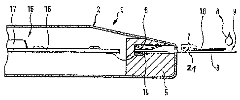
The test element analytical system 1 shown in figure 1 consists of an
evaluation
instrument 2 and a test element 3.
The evaluation instrument 2 has a test element holder 5 which positions a test
element 3 in the measuring position shown in figure 1. The test element 3 is
fixed in
the measuring position by suitable means for example by a spring element 6.
In order to carry out a measurement, sample liquid is brought into the
measuring
zone 7 of the test element 3. In the embodiment shown this occurs by applying
a drop
of liquid 8 to the sample application zone 9 provided at the end of the test
element 3
CA 02559195 2006-09-08
-20-
and transporting it from this position through a transport zone 10, for
example a
capillary gap, to the measuring zone 7. A reagent layer 21 is located in the
measuring
zone 7 which is dissolved by the sample liquid and reacts with its components.
The reaction results in a detectable change in the measuring zone 7. In the
case of an
electrochemical test element the measured electrical quantity is determined by
means
of the electrodes shown in figure 2 that are provided in the measuring zone.
In the
measuring position an electrical contact is made between the test element 3
and the
contact element 14 of the test element holder 5. The contact element 14 is
connected
to measuring and evaluation electronics 15 which are highly integrated in
order to
achieve a very compact construction and high degree of reliability. In the
case shown
they are essentially composed of a printed circuit board 16 and a special IC
17. To
this extent the analytical system has a conventional construction and needs no
further
explanation.
Figure 2 shows a partial view of an exemplary test element 3 for
electrochemical
analytical methods.
An analyte-specific change is detected as part of the analyte determination
within the
measuring zone 7. In the case shown of an electrochemical test element a
measured
electrical quantity is measured by means of electrodes 4 provided in the
measuring
zone. The electrical signal is passed onto the contact areas 11 via the
conductor paths
13. These contact areas make direct contact with the contact areas of the
contact
element 12 when the test element 3 is plugged into the test element holder 5
and thus
make an electrical contact between test element and evaluation instrument. The
test
element that is shown here is only an exemplary and minimalized embodiment of
a
test strip. Test elements with other arrangements of electrodes and conductor
paths
and with several electrodes, for example reference electrodes, and additional
structures such as sample application and transport zones or special reaction
areas
can also be used within the scope of the present invention.
Figure 3 shows a detailed view of a contact element according to the
invention.
The test element 3 is introduced into the test element holder 5 by insertion.
Electrical
contact is made between the contact areas of the contact element 12 and the
contact
CA 02559195 2006-09-08
-21 -
area of the test element 11. In this case the contact element 14 is especially
designed
such that it has elastic properties and thus exerts a defined contact pressure
on the
test element 3. This is exhibited by a particularly preferred embodiment in
which the
contact element 14 ensures the electrical contacting as well as the
positioning and
fixing of the test element. In contrast the functions of electrical contacting
and
positioning/fixing are divided between two different components in figure 1,
namely
the spring element 6 and the contact element 14.
Figure 4 shows a detailed view of a cross-section of a contact element coated
with a
hard material in the region of the contact area. The hard material coating 20
is in this
case applied to the base material 18 of the contact element and an
intermediate layer
19 is present in this case between the two layers which in particular can be
designed
as a bonding or protective layer. The hard material coating 20 functionally
corresponds to the contact area of the contact element 12.
Examples:
For use in test element analytical systems it is important that the contact
connections
between the test elements and analytical instrument still guarantee defined
and low
transition resistances even after numerous insertions in order to ensure an
exact and
reproducible analyte determination by the test element analyzer.
Example 1: Contact elements with chromium nitride-coated contact areas
a) microscopic examination of the surface
In order to demonstrate the advantageous effect of hard material surfaces
according
to the invention as contact areas in an electrical contact connection of a
test element
analytical system, the contact areas of such plug-in connections were coated
with
chromium nitride. A 480 nm thick chromium nitride layer was applied to the
contact
areas of the plug-in connection using a PVD process. In each case new test
elements
were plugged 480 times into plug-in connections coated in this manner. These
test
elements had gold layers having a thickness of 50 nm as contact areas which
were
applied to a plastic foil. After 480 insertions the picture of damage to the
contact
areas of the plug-in connection as well as to the individual contact areas of
the test
CA 02559195 2006-09-08
-22-
elements were evaluated microscopically. As a comparison 480 test elements
were
inserted into conventional, non-hard material-coated plug-in connections with
contact areas made of electropolished palladium under otherwise identical
conditions
and also microscopically evaluated.
The picture of damage to the contact areas of the test elements which were
inserted
into conventional plug-in connections having contact areas made of
electropolished
palladium exhibited a great amount of material erosion and deformations of the
gold
layer of the test elements. These were the result of the relative movement of
the test
element across the plug-in connection. Thus the gold layer on the contact
areas and
conductor paths of the test element are highly deformed by the second contact
area of
the plug-in connection that moves relatively across it. This deformation can
be to
such an extent that in some areas the gold layer is abraded down to the
plastic foil
due to the second contact area scratching across it. As a result the
electrical contact is
interrupted in these cases and hence an analyte determination is impossible.
In contrast the picture of damage to the contact areas of the test elements
which were
inserted into plug-in connections according to the invention whose contact
areas
were coated with 480 nm chromium nitride exhibited considerably less damage.
Microscopic observation of the contact areas of the test element showed that
the
contact areas of the test element were deformed to a much lesser extent than
with the
plug-in connections that were not coated with a hard material. In particular
larger
material erosions or changes in the layer thicknesses were not observed and
the gold
layer of the contact areas and conductor paths remained in all cases as a
continuous
layer. The microscopic picture of darriage showed a more uniform deformation
of the
gold layer in the form of a flat channel with relatively constant and small
depths
without material being strongly or even completely eroded at particular sites.
The microscopic picture of damage of conventional contact areas of contact
elements
of plug-in connections which were not coated with a hard material after 480
insertions was also much worse than the microscopic picture of damage of
corresponding contact areas with a hard material surface according to the
invention
consisting of 480 nm chromium nitride.
CA 02559195 2006-09-08
-23-
The non-hard material-coated contact areas of the contact elements of the
control
plug-in connections exhibited considerable wear of the metal layer when
observed
under the microscope which resulted in a complete abrasion of the metal layer
at
some sites. In some cases deposits of surface materials of the inserted test
elements
were also observed on the contact areas of the plug-in connections.
In contrast the chromium nitride-coated contact areas of the contact elements
according to the invention exhibited no significant signs of wear even after
such
frequent insertions. In particular the chromium nitride layer was observed to
have an
intact and continuous surface and there was a reduced deposition of the
electrode
material of the test strip.
b) electrical transition resistances
When the electrical transition resistances were measured between the test
element and
contact element of the plug-in connection it was observed that, especially
after many
insertions, the contact elements coated with a hard material enable
considerably more
reproducible electrical contact connections that are less susceptible to
interference than
conventional contact elements without such a hard material surface. For this
purpose
in each case 480 new test elements of the type described above which had a 50
nm thick
gold layer as the electrode material were either inserted into plug-in
connections whose
contact areas were coated with 480 nni chromium nitride or into plug-in
connections
with non-hard material coated contact areas made of clectropolished palladium
(controls) and in each case the transition resistances were determined between
8
electrode areas of a test element and the plug-in connection so that in each
case 3940
values of transition resistances were obtained for hard material-coated
contact areas
and non-hard material-coated control contact areas.
Figure 5a shows a frequency distribution of the transition resistances
determined in
this manner for contact elements with non-hard material-coated contact areas
made
of electropolished palladium. The measured transition resistance R is plotted
on the
abscissa in 0.1 Ohm ranges and the frequency f of the measured transition
resistances
normalized to the highest frequency value (= 100) are plotted on the ordinate.
CA 02559195 2006-09-08
-24-
This shows that most of the transition resistances in these controls are in
the low
value range between 0 and 10 Ohm but a not inconsiderable number of measured
transition resistances reach an "infinite" magnitude. Such transition
resistances
measured as "infinite" mean that there is no electrical contact between the
respective
contact element of the plug-in connection and the contact area of the test
element
and no resistance can be measured. These values are marked by the arrow on the
right side of figure 5a. The evaluation of the individually measured
transition
resistances showed that 32 of the measured transition resistances were larger
than
50 Ohm. A transition value of 50 Ohm is regarded as a threshold value in test
element
analytical systems constructed in this manner below which a measurement can
still be
regarded as reliable. 16 of the examined 480 test elements, however, had at
least one
transition resistance value above 50 Ohm. This resulted in a high error rate
of 3.3 %
of the measured test elements so that such contact elements are of only
limited
suitability for a permanent and reproducible use in test element analytical
systems.
Figure 5b shows a frequency distribution of the measured transition
resistances for
contact elements according to the invention which were hard material-coated
with
480 nm chromium nitride.
It can be clearly seen that no values larger than 50 Ohm were observed in the
determination of the 3840 transition resistances. Although more resistance
values
were between 10 and 50 Ohio, none of the measured 3840 values were above the
threshold value of 50 Ohm and none of the transition resistance values were
"infinite" as with the non-hard material-coated contact areas. Thus such
contact
connections can he used to transfer electrical signals reproducibly and
exactly for
many plug-in operations. The use of such contact connections according to the
invention in test element analyzers thus has the advantage that in such
systems
reproducible and exact analyte determinations can he carried out especially
even after
numerous insertions.
Example 2: Contact elements with titanium nitride-coated contact areas
Analogous experiments were carried out with plug-in connections with contact
elements whose contact areas had a hard material surface according to the
invention
CA 02559195 2006-09-08
-25-
consisting of 120 nm titanium aluminium nitride which was also applied by
means of
a PVD process.
a) microscopic examination of the surface
Also in this case it turned out that a hard material-coating of the contact
areas of the
plug-in connection with titanium aluminium nitride according to the invention
considerably improves the picture of damage to the contact areas of the test
elements.
Microscopic observation of the respective contact areas of the test element
showed
that the contact area of the test element was deformed but to a much lesser
extent
than with the controls that were not coated with a hard material. In
particular larger
material erosions or changes in the layer thicknesses were not observed and
the gold
layer of the contact areas and conductor paths remained as a continuous layer.
The
microscopic picture of damage showed, similar to a chromium nitride-coated
contact
area, a more uniform deformation of the gold layer in the form of a flat
channel with
a relatively constant and small depth without material being strongly or even
completely eroded at particular sites.
Also the damage to the titanium aluminium nitride coating itself was much less
after
480 insertions than with the non-hard material coated control plug-in
connections.
The titanium aluminium nitride-coated contact areas of the plug-in connections
according to the invention exhibited no significant signs of wear or deposits
even
after frequent insertions. In particular the surface of the titanium nitride
layer was
observed to still be intact and continuous.
b) electrical transition resistances
In the measurement of transition resistances, like the measurement in example
lb), it
turned out that contact areas of plug-in connections coated with titanium
aluminium
nitride enable considerably more reproducible electrical contact connections
between
the plug-in connection and test element that are considerably less susceptible
to
interference than conventional plug-in connections without such a hard
material
surface. A particular advantage of this embodiment is that in addition to a
very high
contact reliability (no values above 50 Ohm) compared to the chromium nitride-
CA 02559195 2006-09-08
-26-
coated contact areas from example 1, the values of the measured transition
resistances are even considerably lower.
Figure 5c shows a frequency distribution of the measured transition
resistances for
contact elements according to the invention with contact areas coated with a
hard
material comprising 120 nm titanium aluminium nitride.
The determination of transition resistances clearly showed that no values were
observed that are larger than 50 Ohm. Also almost all measured resistance
values
were between 1 and 3 Ohm and thus even considerably lower than with the non-
hard
material-coated contact areas of example 1 (fig. 5a). Thus such contact
connections
can be used to transfer electrical signals reproducibly and exactly for many
plug-in
operations. The use of such contact connections according to the invention in
test
element analyzers thus has the advantage that in such systems reproducible and
exact
analyte determinations can be carried out especially even after numerous
insertions.
The very low transition resistances in the case of contact elements with
titanium
aluminium nitride-coated contact areas have the additional advantage that the
actual
measurement signal is hardly affected by the transition resistance and thus it
is
possible to carry out particularly exact analyte determinations even with low
measurement signals.
Example 3: Change in the transition resistances from example 1 and 2 after
numerous
plug-in processes:
For reproducible use in test element analytical systems over a long time
period and
for many measurement cycles it is also important that the transition
resistances are as
constant as possible and do not exhibit an extreme running-in or wear
behaviour
which is characterized by initially high and then decreasing resistance values
or
initially low and then increasing resistance values.
Control plug-in connections with contact areas made of electropolished
palladium
exhibited scattered contact failures characterized by "infinite" resistance
values over
the 480 insertions of a new test element in each case over the entire time
period. Such
randomly scattered contact failures are disadvantageous especially for the
CA 02559195 2006-09-08
-27-
reproducibility of the measurement result since a measurement error must
always be
expected with a certain probability.
Plug-in connections with contact areas which were coated with 480 nm chromium
nitride exhibited an increase in the transition resistances with an increasing
number
of insertions. In such test systems it can therefore be advantageous to
replace the
contact elements coated with the hard material after a certain number of
measurements in order to ensure a constant high accuracy of measurement. For
this
reason the present invention also encompasses such hard material-coated
contact
elements and contact connections as well as evaluation instruments which
contain
such contact elements and contact connections coated with the hard material.
Plug-in connections with contact areas which were coated with 120 nm titanium
aluminium nitride initially exhibited higher transition resistances which
decreased to
a very low resistance level with an increasing number of insertions. This
observation
shows that, in contrast to a chromium nitride coating, very reproducible and
low
transition resistances can be achieved especially even after many insertions
by use of a
titanium aluminium nitride coating and such coatings of contact areas are
especially
suitable for test element analytical systems which should enable exact analyte
determinations over a very long period of use and very many measurements.
This shows that it is also possible to adapt the test element analytical
system to the
requirements of the respective field of application especially with regard to
the life-
time and exactness of the analyte determination by selection of the material
for the
hard material surface.