Note: Descriptions are shown in the official language in which they were submitted.
CA 02559681 2006-09-14
- 1 -
TITLE OF THE INVENTION
CONTROL UNIT CONNECTABLE TO EXPANSION UNIT
BACKGROUND OF THE INVENTION
The invention relates to an information processing
apparatus with a control unit used connected to a
motherboard, and more particularly to a control unit
connectable to an expansion unit and suitable for
mounting the expansion unit on the information
processing apparatus for function extension.
In general, information processing apparatuses
represented by private branch exchanges (PBXs) are
provided with a plurality of printed circuit boards
including a control unit (control board) for
controlling the entire apparatus. These boards are
generally connected to the motherboard using
connectors.
In information processing apparatuses of this
type, there is a case where the functionality of the
control unit needs to be extended. In general, to
extend the functionality of the control unit, an
expansion unit (expansion board) is used. In the prior
art, during control unit expansion work, the expansion
unit is connected to the motherboard and control unit,
using connectors, whereby it is mounted on the
information processing apparatus. In this state, the
control unit and expansion unit cooperate to exhibit
extended control functionality. In this prior art
CA 02559681 2006-09-14
- 2 -
(first prior art), when the control unit is correctly
connected to the motherboard, it is automatically
released from its reset state and becomes operable upon
the turn-on of the apparatus.
On the other hand, Jpn. Pat. Appln. KOKAI
Publication No. 2003-318576 (prior art document), for
example, discloses an information processing system in
which a monitor board and interface board are connected
to a motherboard (backplane) via connectors. In the
technique (second prior art) described in this
document, the monitor board always or regularly
monitors the operation state of the interface board.
The CPU section on the monitor board determines whether
the interface board is correctly connected to the
motherboard, depending upon whether the potential of a
preset line is high (H). If the interface board is not
correctly connected to the motherboard, the monitor
board determines that no interface board exists. In
contrast, if the interface board is correctly connected
to the motherboard, the monitor board and interface
board hold mount information indicating this fact.
Based on the mount information, the control section on
the interface board releases the reset state of the
circuit mounted on the interface board, under the
control of the CPU section of the monitor board.
Because of incorrect control unit expansion work,
an incomplete connection state may occur in which, for
CA 02559681 2006-09-14
- 3 -
example, the expansion unit is connected to the control
unit, but not to the motherboard. Even in such an
incomplete connection state, however, in the first
prior art, the reset state of the control unit is
released if the control unit is correctly connected to
the motherboard. In this case, since the control unit
is operable, it is difficult for the worker to
correctly determine whether the control unit expansion
work is completed.
On the other hand, in the second prior art, the
monitor board can determine whether the interface board
is correctly connected to the motherboard. It is
possible to impart the determination function of the
monitor board to the control unit of the first prior
art in order to enable the control unit to determine
whether the expansion unit is correctly connected to
the motherboard. In this case, when the expansion unit
is not correctly connected to the motherboard, the
control unit is prevented from being released from its
reset state.
However, in the technique acquired by applying the
second prior art to the first prior art, the control
unit may operate in the following manner. Namely, even
if the control unit is used singly without any
expansion unit, the control unit determines that the
expansion unit is not correctly connected to the
motherboard, with the result that the reset state of
CA 02559681 2006-09-14
- 4 -
the control unit is not released.
BRIEF SUMMARY OF THE INVENTION
In accordance with an embodiment of the invention,
there is provided a control unit permitted to be
connected to a motherboard, and permitted to extend
functionality thereof when the control unit is
connected to an expansion unit. The control unit
comprises a first connector to be connected to the
motherboard; a connection detection circuit which
detects a first state in which the first connector is
connected to the motherboard; a second connector to be
connected to the expansion unit and including a
particular signal pin, the particular signal pin
receiving, from the expansion unit, a particular signal
which assumes a particular logical state in a second
state in which the expansion unit is connected to the
motherboard; a state-setting unit which sets the
particular signal pin to the particular logical state
when the particular signal is not sent to the
particular signal pin; and a reset-releasing circuit
which releases the control unit from a reset state upon
detection of the first state by the connection
detection circuit, the reset-releasing circuit
preventing the reset state of the control unit from
being released regardless of whether the connection
detection circuit detects the first state, when the
particular signal pin assumes a logical state different
CA 02559681 2006-09-14
- 5 -
from the particular logical state.
BRIEF DESCRIPTION OF THE SEVERAL VIEWS OF THE DRAWING
A general architecture that implements the various
feature of the invention will now be described with
reference to the drawings. The drawings and the
associated descriptions are provided to illustrate
embodiments of the invention and not to limit the scope
of the invention.
FIG. 1 is a block diagram illustrating an
exemplary configuration of the essential part of a
private branch exchange according to a first embodiment
of the invention;
FIG. 2 is a perspective view illustrating an
exemplary mount structure of the peripheral portion of
a motherboard employed in the private branch exchange
of FIG. 1; and
FIG. 3 is a block diagram illustrating an
exemplary configuration of the essential part of a
private branch exchange according to a second
embodiment of the invention.
DETAILED DESCRIPTION OF THE INVENTION
Embodiments of the invention will be described
with reference to the accompanying drawings.
[First Embodiment]
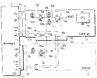
FIG. 1 shows an exemplary configuration of the
essential part of a private branch exchange according
to a first embodiment of the invention. In FIG. 1, one
CA 02559681 2006-09-14
- 6 -
connector 111 of a motherboard 11 is connected to one
connector (first connector) 121 of a control unit 12.
The motherboard 11 is also connected to an interface
unit (not shown) to be controlled by the control unit
12.
The connector 121 of the control unit 12 includes
signal pins for connecting the control unit 12 to the
motherboard 11. The control unit 12 has, as well as
the connector 121, a connector (second connector) 122
that includes signal pins for connecting the control
unit 12 to an expansion unit 13. When the control unit
12 is connected to a connector 131 included in the
expansion unit 13 via the connector 122, it extends its
functionality. In this case, however, it is necessary
to also connect the expansion unit 13 to the other
connector 112 of the motherboard 11 via a connector
section 20 included in the expansion unit 13. Namely,
the expansion unit 13 is constructed to extend the
functionality of the control unit 12 when it is
connected to the motherboard 11 and control unit 12.
FIG. 2 shows an exemplary mount structure of the
peripheral portion of the motherboard 11 in the private
branch exchange of FIG, 1. The connector section 20
comprises the other connector 132 of the expansion unit
13, a flexible printed circuit board (FPC board) 21,
and an extension board 22. The extension board 22
includes connectors 221 and 222. The connectors 122
CA 02559681 2006-09-14
and 131 of the control unit 12 and expansion unit 13
are provided on surfaces of the control unit 12 and
expansion unit 13, respectively, so that the control
unit 12 and expansion unit 13 can be connected with
their surfaces opposing each other.
To mount the expansion unit 13 on the motherboard
11, the connector 132 of the expansion unit 13 is
connected to the connector 221 of the extension board
22 by the FPC board 21, and the connector 222 of the
extension board 22 is connected to the connector 112 of
the motherboard 11, whereby the expansion unit 13 is
connected to the connector 112 of the motherboard 11
via the connector section 20. In the first embodiment,
the connector section 20 is used to mount the expansion
unit 13 on the motherboard 11 in light of the
restricted mount space of the expansion unit 13.
However, the expansion unit 13 can be directly
connected to the motherboard 11 using a connector
similar to the connector 121 of the control unit 12.
Referring again to FIG. 1, the connector 121 of
the control unit 12 includes signal pins 121a, 121b and
121c. The signal pins 121a, 121b and 121c are
connected to a ground pin llla, power supply pin 111b
and ground pin 111c of the connector 111 of the
motherboard 11, respectively.
In the control unit 12, the signal pin 121a is
connected to a connection detection circuit 123. From
CA 02559681 2006-09-14
_ g
the logical state of the signal pin 121a, the
connection detection circuit 123 detects a first state
in which the connector 121 of the control unit 12 is
connected to the motherboard 11. The connection
detection circuit 123 is formed of an inverter 123a as
a first logic circuit. The input of the inverter 123a
is connected to the signal pin 121a. In the first
state, the signal level of the signal pin 121a is low,
since the signal pin 121a is connected to the ground
pin llla of the connector 111. In the first
embodiment, the logical state (logical value) assumed
when the signal level is low is defined as logic "0",
and that assumed when the signal level is high is
defined as logic "1". Accordingly, the logical state
of the input of the inverter 123a is logic "0" in the
first state. In accordance with the logical state of
the input, the inverter 123a outputs a detection signal
(first detection signal) 124 acquired by inverting the
logical state. The detection signal 124 assumes a
first logical state, e.g., logic "1", indicating the
detection of the first state when the connector 121 is
connected to the motherboard 11. In contrast, the
detection signal 124 assumes a second logical state,
e.g., logic "0", which differs from the first logical
state, when the connector 121 is disconnected from the
motherboard 11.
The connector 122 of the control unit 12 includes
CA 02559681 2006-09-14
_ g
signal pins 122a, 122b and 122c. The signal pin 122a
receives a detection signal 134 from an inverter 133a,
described later, incorporated in the expansion unit 13,
when a third state in which the connector 122 of the
control unit 12 is connected to the expansion unit 13
is assumed. The detection signal 134 assumes a
particular logical state, e.g., logic ~~1", when a
second state in which the expansion unit 13 is
connected to the motherboard 11 is assumed.
The connector 131 of the expansion unit 13
includes signal pins 131a, 131b and 131c. In the third
state, the signal pins 131a, 131b and 131c are
connected to the signal pins 122a, 122b and 122c of the
connector 122 of the ccntrol unit 12, respectively.
In the first state, the signal pins 122b and 122c
of the connector 122 of the control unit 12 are
connected to the power supply pin lllb and ground pin
111c of the connector 111 of the motherboard 11 via the
signal pins 121b and 121c of the connector 121 of the
control unit 12, respectively. Further, in the second
state, the signal pins 131b and 131c of the connector
131 of the expansion unit 13 are connected to the power
supply pin 112b and ground pin 112c of the connector
112 of the motherboard 11 via the connector section 20,
respectively.
The expansion unit 13 includes a connection
detection circuit 133 similar to the connection
CA 02559681 2006-09-14
- 10 -
detection circuit 123. The connection detection
circuit 133 detects the second state in which the
expansion unit 13 is connected to the motherboard 11.
The connection detection circuit 133 is formed of an
inverter 133a. The input of the inverter 133a is
connected to the ground pin 112a of the connector 112
of the motherboard 11 via the connector section 20.
Accordingly, in the second state, the signal level
(logical state) of the input of the inverter 133 is low
(assumes logic "0"). In accordance with the logical
state of the input, the inverter 133a outputs, to the
signal pin 131a, the detection signal 134 acquired by
inverting the logical state. In the first embodiment,
the input of the inverter 133a is pulled up via a pull-
up resistor 135.
In the control unit 12, the signal pin 122a of the
connector 122 is connected to a reset-releasing circuit
125, along with the output of the inverter 123a. The
reset-releasing circuit 125 releases the reset state of
the control unit 12 upon detection of the first state
indicated by the detection signal 124 output from the
inverter 123a. However, in the following case, the
reset-releasing circuit 125 does not release the reset
state of the control unit 12 even if the first state is
detected:
In the third state in which the connector 122 of
the control unit 12 is connected to the expansion unit
CA 02559681 2006-09-14
- 11 -
13, the reset-releasing circuit 125 receives the
detection signal 134 from the inverter 133a of the
expansion unit 13 via the signal pin 122a of the
connector 122. When the logical state of the signal
pin 122a is logic "0" that does not indicate the second
state, the reset-releasing circuit 125 does not release
the reset state of the control unit 12 regardless of
whether the detection signal 124 indicating the
detection of the first state is output from the
inverter 123a (i.e., the first state is detected by the
connection detection circuit 123).
The reset-releasing circuit 125 comprises, for
example, a 2-input AND gate (second logic circuit)
125a. The respective two inputs of the AND gate 125a
are connected to the output of the inverter 123a and
the signal pin 122a. The respective two inputs of the
AND gate 125a are pulled up by the pull-up resistors
(state-setting units) 126a and 126b. The AND gate 125a
outputs a reset-releasing signal /RESET of logic "1"
only if the detection signal 124 output from the
inverter 123a assumes logic "1" (first logical state),
and the logical state of the signal pin 122a is logic
"1" (particular logical state). The reset-releasing
signal /RESET of logic "1" is used to release the reset
state of a CPU 127 for executing telephone exchange
processing.
In the work for the function extension of the
CA 02559681 2006-09-14
- 12 -
control unit 12, suppose that the connectors 121 and
122 of the control unit 12 are connected to the
motherboard 11 and expansion unit 13, respectively, but
that the connection of the expansion unit 13 to the
motherboard 11 has failed. In this incomplete
connection state (first connection state), the
detection signal 124 output from the inverter 123a of
the control unit 12 assumes logic "1", whereas the
detection signal 134 output from the inverter 133a of
the expansion unit 13 assumes logic ~~0". The detection
signal 134 of logic ~~0" is sent to the signal pin 122a
of the connector 122 of the control unit 12 via the
signal pin 131a of the connector 131 of the expansion
unit 13. As a result, the signal pin 122a assumes
logic ~~0". At this time, the output of the effective
reset-releasing signal /RESET of logic ~~1" from the AND
gate 125a is prevented. Namely, the CPU 127 is
prevented from being operable in an incomplete
connection state.
As described above, in the above-mentioned
incomplete connection state, the CPU 127 is prevented
from being released from its reset state. Namely, even
in the first or third state, if the second state is not
established, i.e., if the signal pin 122a assumes logic
~~0", it is determined that the work for the function
extension of the control unit 12 is not completed,
thereby preventing the CPU 127 (control unit 12) from
CA 02559681 2006-09-14
- 13 -
being released from its reset state.
A description will now be given of the case where
the connector 121 of the control unit 12 is connected
to the motherboard 11, the connector 122 of the control
unit 12 is connected to the expansion unit 13, and the
expansion unit 13 is connected to the motherboard 11.
In this complete connection state, the detection signal
124 and signal pin 122a assume logic "1". At this
time, the AND gate 125a outputs the effective reset-
releasing signal /RESET of logic "1", thereby releasing
the reset state of the CPU 127 (control unit 12).
Namely, in the first embodiment, when the first to
third states are simultaneously established, it is
determined that the work for the function extension of
the control unit 12 is completed, thereby releasing the
reset state of the CPU 127. As a result, the worker
can further accurately determine, than in the prior
art, the completion of the work for the function
extension of the control unit 12.
After the reset state is released, the CPU 127
executes telephone exchange processing. At this time,
the CPU 127 can extend its functionality by utilizing
the expansion unit 13. Specifically, in the first
embodiment, the CPU 127 can increase the number of
ports to support from 192 to 672, for example.
A description will be given of the case where the
first state is established, the second state is not
CA 02559681 2006-09-14
- 14 -
established, and the third state is not established.
In this case, the signal pin 122a is disconnected from
the signal pin 131a of the connector 131 of the
expansion unit 13. Accordingly, the detection signal
134 output from the inverter 133a of the expansion unit
13 is not sent to the signal pin 122a. The input of
the AND gate 125a connected to the signal pin 122a is
pulled up via the resistor 126b. Therefore, when the
detection signal 134 output from the inverter 133a of
the expansion unit 13 is not sent to the signal pin
122a, the input (signal pin 122a) of the AND gate 125a
assumes a state of logic "1". Further, in the first
state, the detection signal 124 assumes logic "1". At
this time, the AND gate 125a outputs the effective
reset-releasing signal /RESET of logic "1". Thus, when
the first state is established, the second state is not
established, and the third state is not established, it
is determined that the control unit 12 is used singly,
disconnected from the expansion unit 13, whereby the
reset state of the CPU 127 of the control unit 12 is
released.
[Second Embodiment]
FIG. 3 shows an exemplary configuration of the
essential part of a private branch exchange according
to a second embodiment of the invention. In FIG. 3,
elements similar to those of FIG. 1 are denoted by
corresponding reference numbers. In the first
CA 02559681 2006-09-14
- 15 -
embodiment, in an incomplete connection state (first
connection state) in which the first and third states
are simultaneously established, but the second state is
not established, the CPU 127 is prevented from being
released from its reset state. However, in the first
embodiment, even if the first state is established and
the third state is not established, not only the
detection signal 124 but also the signal pin 122a
assume logic "1", regardless of whether the second
state is established. Accordingly, in the first
embodiment, in an incomplete connection state (second
connection state) in which the first and second states
are simultaneously established, but the third state is
not established, the reset state of the CPU 127 is
released.
The second embodiment is characterized in that in
the second connection state in which the first and
second states are simultaneously established, but the
third state is not established, the CPU 127 is
prevented from being released from its reset state, as
in the first connection state in which the first and
third states are simultaneously established, but the
second state is not established.
Specifically, as shown in FIG. 3, the second
embodiment employs a control unit 120 and expansion
unit 130 that correspond to the control unit 12 and
expansion unit 13 in the first embodiment,
CA 02559681 2006-09-14
- 16 -
respectively. The control unit 120 includes connectors
121 and 122 like the control unit 12, and the expansion
unit 130 includes a connector 131 and connection
section 20 like the expansion unit 13.
Like the control unit 12, the control unit 120 is
connected to the motherboard 11 and expansion unit 130.
Further, like the expansion unit 13, the expansion unit
130 is connected to the motherboard 11. In FIG. 2, if
necessary, the control unit 12 and expansion unit 13
may be replaced with the control unit 120 and expansion
unit 130, respectively. Further, in each of the first
to third states, the control unit 12 and expansion unit
13 may be replaced with the control unit 120 and
expansion unit 130, respectively. Namely, in the
second embodiment, the state in which the connector 121
of the control unit 120 is connected to the motherboard
11 is called a first state, the state in which the
expansion unit 130 is connected to the motherboard 11
is called a second state, and the state in which the
connector 122 of the control unit 120 is connected to
the expansion unit 130 is called a third state.
In the second state, the detection signal 134
output from the inverter 133a of the expansion unit 130
is sent to a signal pin 112d incorporated in the
connector 112 of the motherboard 11 via the connector
section 20, which differs from the first embodiment.
The signal pin 112d is connected to a signal pin 111d
CA 02559681 2006-09-14
- 17 -
incorporated in the connector 111 of the motherboard 11
via, for example, a spare signal line 113 on the
motherboard 11. In the first state, the signal pin
111d is connected to a signal pin 121d incorporated in
the connector 121 of the control unit 120. In the
second embodiment, the signal pins 111d and 112d are
spare pins beforehand connected to the signal line 113.
The expansion unit 130 includes a connection
detection circuit 136 which detects the third state.
The connection detection circuit 136 is formed of an
inverter 136a. The input of the inverter 136a is
connected to the signal pin 131c of the expansion unit
130. In the third state, the signal pin 131c is
connected to the signal pin 122c of the connector 122
of the control unit 120. In the first state, the
signal pin 122c is connected to the ground pin 111c of
the connector 111 of the motherboard 11. In the second
state, the signal pin 131c is also connected to the
ground pin 112c of the connector 112 of the motherboard
11. The inverter 136a outputs a detection signal 137
of logic "1" to the signal pin 131d of the connector
131 when the signal pin 131c assumes logic "0". In the
third state, the detection signal 137 is sent to a
signal pin 122d incorporated in the connector 122 of
the control unit 120.
The signal pin 131c assumes the state of logic "0"
at least when the first and third states are
CA 02559681 2006-09-14
- 18 -
simultaneously established, or when the second state is
established. In this case, the inverter 136a outputs a
detection signal 137 of logic "1". However, when the
third state is not established, the detection signal
137 is not sent to the signal pin 122d of the connector
122. It is in the third state that the detection
signal 137 is sent to the signal pin 122d of the
connector 122 to set the signal pin 122d to logic "1".
From this, the control unit 120 recognizes the
detection signal 137 as a signal indicating whether the
third state is detected.
The reset-releasing circuit 125 of the control
unit 120 includes a particular-state detection circuit
141, which differs from the first embodiment. The
particular-state detection circuit 141 detects a
particular state in which the logical state of the
signal pin 121d indicates the second state, and the
logical state of the signal pin 122d indicates the
third state, or in which the logical state of the
signal pin 121d does not indicate the second state, and
the logical state of the signal pin 122d does not
indicate the third state. Upon the detection of the
first state by the connection detection circuit 123, or
upon the detection of the particular state by the
particular-state detection circuit 141, the reset-
releasing circuit 125 releases the reset state of the
control unit 120 (CPU 127).
CA 02559681 2006-09-14
- 19 -
The signal level of the signal pin 121d is pulled
down via a pull-down resistor (first-state-setting
unit) 128a, and the signal level of the signal pin 122d
is pulled down via a pull-down resistor (second-state-
setting unit) 128b. As a result, the signal pin 121d
assumes a logical state (logic "0") different from the
logical state (logic "1") of the detection signal 134
indicating the detection of the second state, when the
motherboard 11 is connected to the connector 121 of the
control unit 120, but not to the expansion unit 130.
Similarly, the signal pin 122d assumes a logical state
(logic "0") different from the logical state (logic
"1") of the detection signal 137 indicating the
detection of the third state, when the motherboard 11
is connected to the connector 121 of the control unit
120, and the connector 122 of the control unit 120 is
disconnected from the expansion unit 130. Namely,
where the detection signal 134 output from the inverter
133a of the expansion unit 130 is not sent to the
signal pin 121d of the connector 121 via the
motherboard 11, the signal pin 121d is set to logic "0"
via the pull-down resistor 128a. Similarly, where the
detection signal 137 output from the inverter 136a of
the expansion unit 130 is not sent to the signal pin
122d of the connector 122, the signal pin 122d is set
to logic "0" via the pull-down resistor 128b.
The particular-state detection circuit 141 is
CA 02559681 2006-09-14
- 20 -
formed of a 2-input exclusive-OR circuit 141a as a
second logic circuit. The two inputs of the exclusive-
OR circuit 141a are connected to the signal pins 121d
and 1224. The exclusive-OR circuit 141a outputs a
detection signal (second detection signal) 142 of logic
"1" indicating the detection of the particular state
(third logical state), when the signal pin 121d assumes
logic "1" indicating the second state, and the signal
pin 122d assumes logic "1" indicating the third state.
The exclusive-OR circuit l4ia outputs the detection
signal (second detection signal) 142 of logic "1", also
when the signal pin 121d assumes logic "0" indicating
no second state, and the signal pin 122d assumes logic
"0" indicating no third state. In the states other
than the above, the exclusive-OR circuit 141a outputs a
detection signal 142 of logic "0" (indicating a fourth
logical state different from the third one).
The reset-releasing circuit 125 also includes a 2-
input AND gate (third logic circuit) 143 corresponding
to the AND gate 125a in FIG. 1. The two inputs of the
AND gate 143 receive the detection signals 124 and 142
from the inverter 123a and exclusive-OR circuit 141a,
respectively. Like the AND gate 125a, the two inputs
of the AND gates 143 are palled up via the pull-up
resistors (state-setting units) 126a and 126b. The AND
gate 143 outputs a reset-releasing signal /RESET of
logic "1" only if the output (detection signal 124) of
CA 02559681 2006-09-14
- 21 -
the inverter 123a assumes logic "1" (first logical
state) indicating the detection of the first state, and
the output (detection signal 142) of the exclusive-OR
circuit 141a assumes logic "1" (third logical state)
indicating the detection of the particular logical
state.
Suppose here that during the work for the function
extension of the control unit 12, the motherboard 11 is
connected to the connector 121 of the control unit 120
and the expansion unit 130, but the connector 122 of
the control unit 120 is disconnected from the expansion
unit 130. In this incomplete connection state (second
connection state), the output (detection signal 124) of
the inverter 123a assumes logic "1". Further, the
signal pin 121d of the connector 121 assumes logic "1",
and the signal pin 122d of the connector 122 assumes
logic "0". In this case, the output (detection signal
142) of the exclusive-OR circuit 141a assumes logic
"1", thereby preventing the AND gate 125a from
outputting the effective reset-releasing signal /RESET
of logic "1". As a result, the CPU 127 is prevented
from being operable in the incomplete connection state
that cannot be prevented in the first embodiment, i.e.,
the second connection state (in which the first and
second states are established, and the third state is
not established).
In the first and second embodiments, it is assumed
CA 02559681 2006-09-14
- 22 -
that the invention is applied to the control unit of an
in-plane exchange. However, the invention is also
applicable to a control unit for information processing
apparatuses other than in-plane exchanges. It is
sufficient if the control unit is used connected to a
motherboard, and can extend its functionality when it
is connected to an expansion unit.
While certain embodiments of the inventions have
been described, these embodiments have been presented
by way of example only, and are not intended to limit
the scope of the inventions. Indeed, the novel
apparatuses and methods described herein may be
embodied in a variety of other forms; furthermore,
various omissions, substitutions and changes in the
form of the apparatuses and methods described herein
may be made without departing from spirit of the
inventions. The accompanying claims and their
equivalents are intended to cover such forms or
modifications as would fall within the scope and sprit
of the inventions.