Note: Descriptions are shown in the official language in which they were submitted.
CA 02560568 2006-09-19
WO 2005/094536 PCT/US2005/009889
DIGITAL LINEARIZING SYSTEM
CROSS REFERENCE TO OTHER APPLICATIONS
[0001] This application claims priority to U.S. Provisional Patent Application
No. 60/556,550 (Attorney Docket No. OPTIP008+) entitled DIGITAL
LINEARIZING SYSTEM filed March 25, 2004, which is incorporated herein by
reference for all purposes.
BACKGROUND OF THE INVENTION
[0002] In signal processing systems, there is often a need to compensate for
nonlinear distortions introduced by the system. There are many possible
sources for
system nonlinearities, including characteristics of nonlinear components such
as
inductors, capacitors and transistors. Nonlinearities are frequently
introduced when
analog signals are converted to digital. Besides component nonlinearities,
analog-to-
digital converters (ADCs) often have additional sources of nonlinearity, such
as the
sampling capacitors' time constants, gain error in amplifiers and imprecision
in the
comparator levels.
[0003] Nonlinear distortions may depend on many factors such as the input
signal's frequency range, history and rate of change (also referred to "slew
rate"), as
well as external factors such as operating temperature. The difficulties in
modeling
nonlinear distortions lead to difficulties in characterizing and compensating
system
nonlinearities. Existing techniques for characterizing system nonlinearities
such as
Volterra expansion tend to be complex and difficult to implement.
[0004] Furthermore, in some systems, even if a distortion model is found by
using Volterra expansion, it could not be accurately applied due to the
unavailability
of the required inputs. For example, in some communication systems, the
receiver
circuitry may introduce nonlinearities when the input analog signal is
digitized and
demodulated to baseband. The intermediate frequency (IF) signal required by
the
distortion model is often unavailable since the IF signal is directly
demodulated to
baseband when the ADC samples the signal. Applying the baseband signal to the
CA 02560568 2006-09-19
WO 2005/094536 PCT/US2005/009889
distortion model usually means that some of the history and slew rate
information is
lost; therefore, the distortion estimation is less accurate.
[0005] It would be useful to have a way to better compensate for system
nonlinearities even as some of the data required by the distortion model is
not
available as input. It would also be useful if the compensation scheme could
be
applied without requiring special data access.
BRIEF DESCRIPTION OF THE DRAWINGS
[0006] Various embodiments of the invention are disclosed in the following
detailed description and the accompanying drawings.
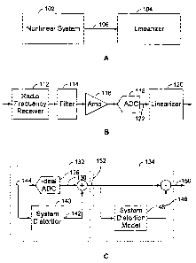
[0007] Figures lA-1C are diagrams illustrating several linearizer
embodiments.
[0008] Figure 2 is a flow chart illustrating an embodiment of a process for
compensating for nonlinear distortion in a digital signal.
[0009] Figures 3A - 3C are signal diagrams illustrating the processing of a
baseband signal according to some linearizer embodiments.
[0010] Figures 4A - 4D are diagrams illustrating the processing of an input
signal within a higher order Nyquist zone.
[0011] Figure S is a block diagram illustrating a linearizer embodiment.
[0012] Figure 6 is a block diagram illustrating the implementation of a linear
processing module embodiment.
[0013] Figure 7 is a diagram illustrating another linear processing module
embodiment.
[0014] Figure 8 is a diagram illustrating another linear processing module
embodiment.
[0015] Figure 9 is a block diagram illustrating a nonlinear processor
embodiment.
2
CA 02560568 2006-09-19
WO 2005/094536 PCT/US2005/009889
DETAILED DESCRIPTION
[0016] The invention can be implemented in numerous ways, including as a
process, an apparatus, a system, a composition of matter, a computer readable
medium such as a computer readable storage medium or a computer network
wherein
program instructions are sent over optical or electronic communication links.
In this
specification, these implementations, or any other form that the invention may
take,
may be referred to as techniques. A component such as a processor or a memory
described as being configured to perform a task includes both a general
component
that is temporarily configured to perform the task at a given time or a
specific
component that is manufactured to perform the task. In general, the order of
the steps
of disclosed processes may be altered within the scope of the invention.
[0017] A detailed description of one or more embodiments of the invention is
provided below along with accompanying figures that illustrate the principles
of the
invention. The invention is described in connection with such embodiments, but
the
invention is not limited to any embodiment. The scope of the invention is
limited
only by the claims and the invention encompasses numerous alternatives,
modifications and equivalents. Numerous specific details are set forth in the
following description in order to provide a thorough understanding of the
invention.
These details are provided for the purpose of example and the invention may be
practiced according to the claims without some or all of these specific
details. For the
purpose of clarity, technical material that is known in the technical fields
related to
the invention has not been described in detail so that the invention is not
unnecessarily
obscured.
[0018] A method and system for compensating nonlinear distortion in a digital
signal is disclosed. In some embodiments, a nominal phase shifted signal is
generated
based on the digital signal. A modeled distortion signal is generated based on
the
digital signal and the nominal phase shifted signal and then subtracted from
the digital
signal. A compensated signal is then generated. A digital signal may result
from an
analog input restricted to a known region of operation (such as a Nyquist
zone). In
some embodiments, the nominal phase shifted signal is generated by
interpolating the
digital signal and taking interpolated values at fractional intervals of the
sampling
period of the digital signal. In some embodiments, the nominal phase shifted
signal is
CA 02560568 2006-09-19
WO 2005/094536 PCT/US2005/009889
generated by up-sampling the digital signal, filtering the up-sampled signal
and
obtaining interpolated values at fractional intervals of the sampling period.
A
derivative calculated based on the digital signal and/or the nominal phase
shifted
signal may also be used by the distortion model. A compensating system
comprising
a distortion model may be configured to correct for nonlinear distortions in
analog to
digital converters, receiver circuits, or any other appropriate system with
nonlinear
distortion in its channel.
[0019] Figures lA-1C are diagrams illustrating several linearizer
embodiments. In Figure 1A, the output of nonlinear system 102 is sent to
linearizer
104, which is configured to compensate for output distortion. The linearizer
can be
implemented as software or firmware code embedded in a processor, a field
programmable date array (FPGA), a programmable digital signal processing (DSP)
engine, an application specific integrated circuit (ASIC), any other
appropriate device
or combinations thereof. In this example, output 106 is treated as an ideal
undistorted
component plus a distortion component. The distortion component is separate
from
ADC quantization error, which is equal to the portion of the analog signal
below the
finest ADC quantization level and typically cannot be reduced for an ADC with
a
predefined number of bits. The distortion component is to be predicted and
corrected
by linearizer 104. As will be shown in more details below, linearizer 104 is
configured to model the distortion component using output 106 of the nonlinear
system.
[0020] Figure 1B is a block diagram of a receiver circuit embodiment that
includes a linearizer. In this example, an analog radio frequency (RF) signal
is
received by radio frequency receiver 112. The signal is demodulated to an IF
signal
by filter 114, and the IF signal is then amplified by amplifier 116. The
signal is
converted to digital by ADC 118. Linearizer 120 is configured to compensate
for
nonlinear distortion in digital signal 122 that results from component
nonlinearities in
receiver chain. Similar to signal 106 of Figure 1 A, signal 122 is treated as
if it
includes an ideal ADC output component and a distortion component. The
linearizer
estimates the distortion based on digital signal 122 and generates a
compensated
output.
CA 02560568 2006-09-19
WO 2005/094536 PCT/US2005/009889
[0021] In Figure 1B, linearizer 120 is trained to model the nonlinear
distortion
introduced by the entire receiver chain. A similar linearizer may also be used
to
compensate for nonlinearities in individual components. For example, in
Figure~lC,
linearizer 134 is coupled to ADC 132 and is configured to compensate for the
nonlinear distortions in the ADC. For purposes of illustration, ADC 132 is
treated as
the equivalent of an ideal analog-to-digital converter 136 that generates an
ideal
digital signal 138, and a distortion module 140 that produces a distortion
component
142. The transfer function of the distortion module may be nonlinear and
varies with
input signal 144, its history and its slew rate.
[0022] Figure 2 is a flow chart illustrating an embodiment of a process for
compensating for nonlinear distortion in a digital signal. For purposes of
illustration,
the following examples discuss in detail the operations and implementations of
various linearizer embodiments that compensate for distortion resulting from
ADCs.
The techniques are also applicable to distortion compensation in transceiver
circuits
or other appropriate signal processing devices.
[0023] In this example, process 200 may be implemented on linearizers 104,
120, 134 or other appropriate devices. The process begins when a digital
signal is
received (202). The digital signal may be the result of an analog-to-digital
converter
such as ADC 132 of Figure 1 C. One or more nominal phase shifted signals based
on
the digital signal are then determined (204). The samples in a nominal phase
shifted
signal correspond to the samples of the ADC input at fractional sampling
phases of
the digital signal (in other words, samples at fractional intervals between
the sampling
periods of the ADC). As will be shown in more details below, the nominal phase
shifted signal may be generated using techniques such as interpolation,
upsampling,
direct modulation, or any other appropriate technique. The received digital
signal and
the nominal phase shifted signal are processed by a distortion module to
generate a
modeled distortion signal (206). The modeled distortion signal is then
subtracted
from the digital signal to generate a compensated signal (208).
[0024] Process 200 may be illustrated using the system embodiment shown in
Figure 1C. ADC output 152 corresponds to the received digital signal (202).
Nominal phase shifted signals based on the digital signal is determined by
system
distortion model 146 (204). The digital signal and the nominal phase shifted
signals
CA 02560568 2006-09-19
WO 2005/094536 PCT/US2005/009889
are processed to generate a modeled distortion signal that is approximately
equal to
distortion signal 142 (206). Estimated distortion 148 is then subtracted from
output
152 of ADC 132 to generate a compensated signal 1 S0.
[0025] In some embodiments, the linearizer generates nominal phase shifted
signals based on the digital signal received. In some embodiments, the
linearizer also
generates derivatives based on the nominal phase shifted signals. The nominal
phase
shifted signals and/or the derivatives are used by the system distortion
model. Figures
3A - 3C are signal diagrams illustrating the processing of a baseband signal
according
to some linearizer embodiments. Figure 3A is a frequency spectrum diagram
illustrating a baseband digital signal 300. In this example, a baseband analog
signal is
sampled and filtered to produce baseband digital signal 300, therefore the
sampling of
the baseband analog signal does not have demodulating effects. Signal 300 is
shown
to include several frequency components. Signal component 302 is the ideal
digital
signal component without nonlinear distortion. Signals 304 and 306 are the
distortion
components.
[0026] The discrete samples of signal 300 in the time domain are shown in
Figure 3B. The samples can be interpolated to reconstruct a signal that
corresponds to
the original baseliand analog signal. Figure 3C shows the interpolated signal
320.
Nominal phase shifted samples at fractional phases of the ADC's sampling phase
are
generated according to interpolated signal 320. In the example shown, for an
ADC
with a sampling period of T, the nominal phase shifted samples are generated
at times
T+~, T+2~ ,..., T+n~, 2T+~, 2T+2~ , ..., 2T+n~, etc., where ~ is a fractional
value of T. The nominal phase shifted samples and the original samples are
sent to
the distortion model as inputs. In the example shown, the distortion model
depends on
the history of the input samples and the derivatives of the input. The nominal
phase
shifted samples provide enhanced history information, and the derivatives
provide
information about the signals rate of change. The additional information
allows the
distortion model to more accurately compute the resulting distortion signal.
[0027] In some embodiments, the input frequencies are restricted to a specific
region. The distortion model can produce better modeled distortion signal if
the
frequency region is lrnown. In the examples below, inputs restricted to
specific
frequency regions referred to as Nyquist zones are discussed in detail. As
used
CA 02560568 2006-09-19
WO 2005/094536 PCT/US2005/009889
herein, the n-th Nyquist zone spans the frequency range between (n 2 1) fs to
2 .fs ,
where fs is equal to the ADC's sampling frequency. The technique is also
applicable
to other types of frequency bands.
(0028] Figures 4A - 4D are diagrams illustrating the processing of an input
signal within a higher order Nyquist zone. Figure 4A is a frequency spectrum
diagram illustrating the input signal. Input 402 is sampled to generate an
aliased
image 404 in the baseband. Figure 4B is a time domain diagram illustrating
input
signal 402 and abased baseband signal 404. The baseband signal includes
samples
such as 412 and 414. As shown in this diagram, certain information contained
in
input signal 402, such as data history and rate of change, is not captured by
the
baseband samples. Although the original signal 402 is not available to the
distortion
model in this example, some of the missing information can be recreated by
digitally
modulating baseband signal 404 to the Nyquist zone where the analog signal
originated. In some embodiments, the digital modulation is done directly by
multiply
the baseband signal with a carrier frequency. In some embodiments, the digital
modulation is achieved by upsampling the baseband signal.
[0029] In Figure 4C, the baseband signal is upsampled. Zeros are inserted
where no sample value is available. The upsampling rate R may vary for
different
embodiments. The choice of R depends on several factors. One of the factors is
the
ratio of the integral sampling period and the required fractional phase. The
upsampling rate should be greater than this ratio. For example, for an
integral
sampling period of T, if the fractional phase ~ is O.1T, then the upsampling
rate
should be greater than 1/0.1 = 10. The upsampling rate also depends on the
spectrum
of the ADC's input signal. In sub-sampling applications, the input signal may
be at a
higher frequency than the ADC sampling rate. In these applications R is chosen
to be
equal to the sub-sampling rate times 1/( ~ /T ). For example, if the ADC's
sampling
rate is 100 MHz, and the input signal lies between 150 MHz and 200 MHz, then
the
sub-sampling rate is 4. This is because 0 - 50 MHz is the frequency range of
the first
Nyquist zone, and 150 - 200 MHz is 4-times higher. If the desired ~ /T = 0.1,
then
the upsampling rate R = 4 / 0.1 = 40. The upsampled signal is interpolated and
band-
pass filtered to reconstruct the signal at an appropriate frequency. The
nominal phase
CA 02560568 2006-09-19
WO 2005/094536 PCT/US2005/009889
shifted signals are then obtained at the desired fractional phase as shown in
Figure
4D.
[0030] Figure 5 is a block diagram illustrating a linearizer embodiment. In
this example, linearizer 500 includes a linear processing module 502 coupled
with a
nonlinear processing module 504. Linear processing module 502 is configured to
estimate the nominal phase shifted symbols such as yn_~ and yn_Z~ , and
derivates
such as yn , yn-~ and y"-2~ . Nonlinear processing module 504 is configured to
implement the distortion model that estimates the distortion based on the
digital
samples, the nominal phase shifted samples and the derivates.
[0031] Figure 6 is a block diagram illustrating the implementation of a linear
processing module embodiment. In this example, linear processing module 502
includes an upsampling module 602 that upsamples digital input y" at a rate of
R.
Returning to signal examples shown in Figures 4B-4D, input yn corresponds to
the
samples shown in Figure 4B. The output of up-sampling module 602 corresponds
to
the signal shown in Figure 4C. Upsampling generates several images of the
baseband
input signal in different frequency regions. A plurality of digital filters
such as digital
filter 604 is used to select an image in an appropriate frequency region. In
this
example, the selected image is located in the same Nyquist zone as the
original analog
signal that is digitized. Thus, the characteristics of filter bank depend on
the desired
Nyquist zone. Low-pass, band-pass and high-pass digital filters may be used to
achieve the desired filter characteristics.
[0032] The outputs of the digital filters are down-sampled by down-samplers
such as 606. During the down-sampling operation, each down-sampler selects
samples that correspond to a desired phase. Figure 4D illustrates the results
of phase
selection according to one embodiment. In the example shown, samples 410a,
410b,
410c, 410d, etc. that correspond to phase 1 are selected to form a nominal
phase
shifted signal yn-~ . Similarly, samples 412a, 412b, 412c, 412d, etc. that
correspond
to phase 2 are selected to form a nominal phase shifted signal yn-2~ . The
difference
between two adjacent phase signals is computed by a differencing module such
as
608. Derivatives such as yn, yn-~ and y"-z~ are computed based on the
difference.
8
CA 02560568 2006-09-19
WO 2005/094536 PCT/US2005/009889
[0033] Figure 7 is a diagram illustrating another linear processing module
embodiment. In this example, the input signal y" is directly sent to a
plurality of
digital filters without up-sampling. The digital filters used in this example
are
decimated versions of the digital filters used in Figure 6. For a given
digital filter, the
decimation is chosen at an appropriate phase to yield a filter output that
corresponds
to a nominal phase shifted signal. The differences between filter outputs of
adjacent
phases provide derivative estimates.
[0034] Figure 8 is a diagram illustrating another linear processing module
embodiment. In this example, two adjacent phase digital filters and their
corresponding differencing modules are combined into a digital Hilbert filter.
The
Hilbert filter has an impulse response that is equivalent to the difference in
the
impulse responses of digital filters having adjacent phases. The output of the
digital
Hilbert filter provides a direct estimate of the signal derivative at the
desired phase.
[0035] Figure 9 is a block diagram illustrating a nonlinear processor
embodiment. In this example, nonlinear processor 900 implements the distortion
model of the ADC. The transfer function of the distortion model may be derived
by
sending test inputs with different amplitudes and varying slew rates to the
ADC. In
some embodiments, the nonlinear transfer function of the distortion model can
be
expressed as the following general form:
~7" = a'o," (Y" ) Y" + ~ ~ ~ + Ll'zN-2,n (Y" ) Y"-zN+z + b" (Y" ) (equation
1),
where Y" is a vector including the integral samples, the fractional samples,
and the
derivatives. An example of Y" is
~',~ _ ~Y" Y"-~ Y"-zg Y" Y"-~ .Y"-zg Y"-i Y"-z Y"-3
[0036] Equation 1 can be viewed as a "linear" convolution between the input
variables and the nonlinear coefficients that are time variant nonlinear
functions of the
input signal. In other words, the function has the form of a linear filter,
but with
nonlinear coefficients. The relative location of input Y" in the multi-
dimensional input
space determines the values of the a~," and b" coefficients. The dependence of
the
filter coefficient values on the input signal vector gives the filter its
nonlinear
property.
9
CA 02560568 2006-09-19
WO 2005/094536 PCT/US2005/009889
[0037] The nonlinear processor output, vn , includes a replica of the original
linear signal vn and the residual uncorrected nonlinear distortion ~n . The
relationship
may be expressed as:
vn - .Yn ~n - vn + ~n ~n - vn + ~n (equation 2),
where ~n = rin - rin . (equation 3).
[0038] In some embodiments, a distortion model similar to equation 1 can be
implemented using one or more minimum-maximum processors and/or absolute value
processors. Details of the implementation are described in U.S. Patent No.
6,856,191,
entitled NONLINEAR FILTER, which is incorporated herein by reference for all
purposes. According to the techniques described, the transfer function of the
distortion model may be expressed as:
K
~n = AT Yn + b + ~ cj a j Yn + ,i3 j I (equation 4).
=I
(0039] Let sign ( a'j Y" + /3j ) _ ~,jn , equation 4 can be rewritten as:
K K K
~n - Cl0 + ~ Cj G~Oj /~'j n yn + . . . + Cl N ~- ~ Cj aN.l ~j n .Yn-N + U + ~
Cj ~j ~j n
j=1 j=1 j=I
(equation 5).
Equation 5 is also equivalent to equation 1.
[0040] The distortion function may be transformed into vector form to
simplify the function and achieve computational reductions. In some
embodiments,
the distortion function is implemented as a low complexity filter with reduced
number
of multiplication operations. The distortion function of equation 4 can be
transformed
as follows:
to
CA 02560568 2006-09-19
WO 2005/094536 PCT/US2005/009889
z Z
~n - '4T Yn + ~J + ~ Cj yn + ~ j + ~ Cj yn-~ + ~j ' ' + K~ Cj ~ yn-N + ~j
j=i j=K~+1 j=KzN_~+1
K K KzN z
=f1T Yn +U+~Cj ~jn(yn '~~J)+ ~Cj /ljn\yn-1 +i'Jl'..+ ~Cj ~j,n~yn-N +~j~
j=~ j=Ki+~ j=KzN-s+1
(equation
6).
Let ~.j,n = sign ( y"-, + ~,~ ) , the function can be further transformed as
K, KzN z K
~n QO + ~ Cj ~j n yn + . . . ~.. a2n-2 -f- ~ Cj ~j n .yn-N + b + ~ Cj ~j ~j n
j=1 j=KzN-~+~ j=1
(equation 7).
[0041] A filter implementing the general form of equation 7 is referred to as
a
first order nonlinear filter since each coefficient is multiplied with terms
ofy to the
first order at most. In some embodiments, cj and c j ~3j are pre-computed and
stored. Since ~,jn is either 1 or -1, the coefficients can be computed without
using
multiplication and the complexity in filter implementation is greatly reduced.
[0042] Other simplifications using vector manipulation are also possible. For
example, another simplified form of the distortion function is expressed as:
~n J O,n 'Yn ~ yn + ~ ~ ~ + J 2N-2,n (Yn ) yn-2N+2 + a0,n \Yn ~ yn + "' + C12N-
2,n \Yn ) yn-2N+2 + Un \Yn
(equation 8),
where each fk,n (Yn ) is a first order nonlinear function
K _
J k.n (Yn ) - Ak Yn + 17k + ~C~ ~ G~~ Yn + ~~ ~ = a0,n (Yn ) yn + ' . . + a N-
Z n (Yn ) yn-ZN+2 + bn (Yn )
j=1
(equation 9).
Accordingly, each coefficient in equation 8 is a nonlinear function of the
input vector
elements and some of the coefficients multiply a power-of two element of the
input
vector or cross-product-of two elements of the input vector. A filter
implementing
this simplified form is referred to as a second order filter.
11
CA 02560568 2006-09-19
WO 2005/094536 PCT/US2005/009889
[0043] In some embodiments, the distortion function is simplified to have
constants in each discrete input region. This simplification results in a zero
order
transfer function. The zero order filter is sometimes referred to as a
"catastrophic"
structure because of the discontinuities in the filter response. A general
form of a zero
order nonlinear filter is expressed as:
K K K
0 0 1 I 2N 2 2N-2
~n =C10 +C11 +...+QZN-2 +b+~Cj/~,j +~Cj/~,j +...+~Cj /~,j
j-1 j=1 j=1
(equation 10).
K
[0044] To implement a zero order nonlinear filter, combinations of ~
c°~,°n ,
j-1
K
C ~ ~,~n , etc. may be pre-computed, stored and retrieved based on the
appropriate
j=1
input. In some embodiments, the coefficient value is determined using an
indicator
that indicates the relative location of the input within the range of possible
inputs.
The indicator is sometimes referred to as a "thermometer code," which is a
vector
having a total of at most one sign change among any two adjacent elements.
(0045] Take the following second order function as an example:
K K
~n - a0 yn + Cll yn-1 + U + ~ C~ yn + N j yn + ~ Cj yn-1 + N j I yn
j=I j-_1
K K K K
0 0 2 1 '1 0 ~0 0 1 ~1 1 L
~j yn + ~Cj ~j yn yn-I + Cl0 +~Cj ~j~j +~Cj ~j~j yn +Ch yn-1 +b
j=I j=1 j=1 j=1
_ 2
- a0l,n yn + al,n yn yn-1 + a0,n yn + al,n yn-1 +
(equation 11 ).
[0046] The input is compared to the set of ,(3K values to determine the
relative
location of the input variable within the range of possible inputs, and the
vector of
~.j,n , denoted as A" . Depending on the input, An may be a vector with terms
that are
+1 only, -1 only, or -1 for the first k terms and +1 for the rest of the
terms. In other
words, An is a thermometer code with at most one sign change among its terms.
For
example, assuming that constants ~3K are distributed across the dynamic range
of
yn E (-1,1 ) and there are 8 values of ~3~ E ~ - ~ - ~ - ~ - ~ ~ ~ ~ ~ ~ . If
12
CA 02560568 2006-09-19
WO 2005/094536 PCT/US2005/009889
yn <-~ , then An =~-1-1-1-1-1-1-1-1 ~. If yn > ~ , then
An = ~+ 1 + 1 + 1 + 1 + 1 + 1 + 1 + 1 ~ . If y" is somewhere in between, An
may have a sign
change. For example, i f yn = 375 , then A n = ~-1-1-1-1-1-1-1 + 1 ~ . If
yn = 1-55 , then A n = [-1-1-1 + 1 + 1 + 1 + 1 + 1 ~ . Since the thermometer
code has
7
K
only 8 values, there are only 8 possible values for ao,,n = ~ co ~o , 8
possible values
j=1
K K K
for a,,n = ~c~ ~,~," , and 64 possible values for ao,n = ao +~c~
~.°/3° +~c~ ~,~/3~ .
%_~ J=~ J=~
[0047] The number of add operations can be reduced by pre-computing the
possible values for coefficients of ao,,n , a,,n , etc. and storing them in
memory. In
this example, the addresses of the coefficients are stored in a lookup table,
which
stores the 8 possibilities of thermometer code An and the corresponding
addresses of
pre-computed coefficients. The coefficients can be retrieved by accessing the
memory addresses that correspond to the appropriate thermometer code entry.
Once
the coefficients ao,,n , a",n etc. .. are read out of memory, the filter
output can be
computed as
~n - a0l,nyn + al,nynyn-1 + a0,nyn + at,nyn-1 + b (equation 12).
This technique is also applicable to zero, first or higher order filters.
[0048] Low complexity nonlinear filters may be implemented based on the
simplified forms. In some embodiments, the low complexity linear filter
includes a
processor coupled to the nonlinear filter, configured to determine the
relative location
of the input variable within a range of possible inputs and to determine a
filter
coefficient of the nonlinear filter using the relative location of the input
variable. The
filter coefficients can be determined without using multiplication operations.
In some
embodiments, filter coefficients for zero order, first order, second order
and/or higher
order filters are pre-computed, stored and retrieved when appropriate. Higher
order
filters can be formed by nesting lower order filters. Details of implementing
a
nonlinear transfer function using low-complexity filter or thermometer code
are
described in U.S. Patent Application No. 11/061,850 (Attorney Docket No.
13
CA 02560568 2006-09-19
WO 2005/094536 PCT/US2005/009889
OPTIP006) entitled LOW-COMPLEXITY NONLINEAR FILTERS, filed 2/18/2005,
which is incorporated herein by reference for all purposes.
[0049] In some embodiments, the distortion model is temperature
compensated. The coefficients of the distortion model at different
temperatures are
predetermined and stored. During operation, the coefficients corresponding to
the
operating temperature is selected to construct an appropriate distortion
correction
filter. In some embodiments, the operating temperature is used to analytically
determine the corresponding coefficients. In other words, the coefficients are
computed based on a function of the input and its history, the derivatives of
the input,
the temperature, the changes in temperature, any other appropriate factors or
a
combination thereof.
[0050] An improved method for compensating nonlinear distortions in digital
signals and a linearizer system have been disclosed. Nonlinearities of ADCs,
receivers, or other systems with nonlinear channel characteristics can be more
effectively compensated by modeling the nonlinearities using the digital
signal, the
nominal phase shifted signals, and their derivatives.
[0051] Although the foregoing embodiments have been described in some
detail for purposes of clarity of understanding, the invention is not limited
to the
details provided. There are many alternative ways of implementing the
invention.
The disclosed embodiments are illustrative and not restrictive.
[0052] WHAT IS CLAIMED IS:
14