Note: Descriptions are shown in the official language in which they were submitted.
CA 02561955 2006-10-02
WO 2005/099028 PCT/US2005/010300
EI~EDDED CAPACITORS USING CONDUCTOR FILLED VIAS
BACKGROUND OF THE INVENTION
Description of the Related Art
Embedded capacitors are currently available in both
printed wire board (PWB) and low temperature co-fired ceramic
(LTCC) technologies. Typically, printed conductors are
deposited on a substrate and used as electrodes for a
capacitor. In some instances, the substrate itself can serve
as the dielectric for the capacitor. In other arrangements, a
via within the substrate can be filled with a dielectric
material.
Using LTCC, the printed conductors are typically
created using a printed thick film process. Etching processes
are typically used for PWB's. In either case, forming
capacitors with tight tolerances can be difficult. In
particular, it is often difficult to precisely control the
area of the electrode. A small difference in electrode area
can significantly change the capacitance of a part.
This problem is compounded further when trying to
simultaneously create both high and low valued capacitors on a
substrate. In such circumstances, high permittivity
dielectrics are typically used so that high value capacitors
can be formed in a volumetrically efficient manner. But the
use of the high permittivity dielectrics requires that very
small electrodes be used to achieve small value capacitors.
Maintaining a tight tolerance on such electrodes can be
extremely difficult. For example, when printing electrodes on
LTCC, variables such as bleed-out, mesh density, and
inaccuracies in the printing process each contribute to
dimensional inaccuracies of the electrodes. Accordingly, a
solution is needed for creating embedded capacitors wherein
tight tolerances can be maintained over a large range of
capacitance values.
1
CA 02561955 2006-10-02
WO 2005/099028 PCT/US2005/010300
SUMMARY OF THE INVENTION
The present invention relates to a method for
manufacturing embedded capacitors. The method can include the
steps of forming at least one bore in a dielectric substrate.
The dielectric substrate can be mechanically punched or laser
cut to form the bore. The bore can be filled with a
conductive material to form a first electrode. Further, a
conductor can be formed on the dielectric substrate, the
conductor not being electrically continuous with the first
electrode. A depth and/or cross sectional area of the bore
can be selected to provide a desired amount of capacitive
coupling between the electrode and the conductor. Further, a
second conductor can be deposited on the dielectric substrate
such that the first conductor is in electrical contact with
the first electrode. At least a second bore can be formed in
the dielectric substrate and filled with a conductive material
to form a second electrode. The second electrode can be
electrically connected to the first electrode.
The first bore can be formed in a first layer of the
dielectric substrate. A second bore can be formed in a second
dielectric layer. The second bore can be filled with a
conductive material. Further, the first and second dielectric
layers can be joined such that the conductive material in the
first bore is electrically continuous with the conductive
material in the second bore. The conductive material in the
first and second bores can form an extended electrode.
The method for manufacturing embedded capacitors
also can include the steps of forming at least one bore in a
first dielectric layer and filling the bore with a conductive
material. A first conductor can be disposed on the first
dielectric layer, the first conductor being in electrical
contact with the first electrode. A second conductor can be
disposed on a second dielectric substrate. The first and
second dielectric layers can be joined such that the first and
2
CA 02561955 2006-10-02
WO 2005/099028 PCT/US2005/010300
second conductors are not electrically continuous. The
dimensions of the first conductor and/or the second conductor
can be selected to provide a desired amount of capacitive
coupling between the first conductor and the second conductor.
The present invention also relates to an embedded
capacitor which can include a substrate having an electrode.
The electrode can include a conductive material which has been
filled into a bore within the substrate. A first conductor
can be disposed on the dielectric substrate. The first
conductor can be in electrical contact with the first
electrode.
The embedded capacitor also can include a conductor
on the substrate which is not electrically continuous with the
first electrode. The depth and/or cross sectional area of the
bore can be selected to provide a desired amount of capacitive
coupling between the electrode and the conductor. A second
electrode also can be provided. The second electrode can
include a conductive material which has been filled into a
second bore within the substrate. The first and second bores
can be electrically connected.
The substrate can include a plurality of dielectric
layers. The first electrode can be disposed within a first
layer of the substrate. A second electrode can be provided
which includes a conductive material that has been filled into
a second bore within a second layer of the substrate. The
first and second bores can be electrically connected.
The present invention also relates to an embedded
capacitor which includes a substrate having a plurality of
dielectric layers. An electrode can be disposed in a first of
the dielectric layers, the electrode including a conductive
material which has been filled into a bore within the
substrate. A first conductor can be disposed on the
dielectric layer, the first conductor being in electrical
contact with the electrode. Further, a second conductor can
3
CA 02561955 2006-10-02
WO 2005/099028 PCT/US2005/010300
be disposed on a second of the dielectric layers, the second
conductor not being electrically continuous with the
electrode. Dimensions of the first and second conductors can
be selected to provide a desired amount of capacitive coupling
between the first and second conductors.
BRIEF DESCRIPTION OF THE DRAWINGS
Fig. 1 is a perspective view of a plurality of
substrate layers having vias for forming embedded capacitors
which are useful for understanding the present invention.
Figs. 2-4 are a series of cross sectional views
taken along section line 2-2 of Fig. 1, the cross sectional
views showing a method of forming embedded capacitors in a
substrate which are useful for understanding the present
invention.
Fig. 5 is a cross sectional view of a substrate
which includes alternate embodiments of embedded capacitors
which are useful for understanding the present invention.
Fig. 6 is a flow chart of a method of manufacturing
embedded capacitors in a substrate which are useful for
understanding the present invention.
DETAINED DESCRIPTION OF THE PREFERRED EMBODIMENTS
The present invention provides a substrate having
embedded capacitors formed therein. Notably, since the
capacitors are formed within the substrate, a greater amount
of substrate surface area is available for positioning of
other components. Moreover, the size of a substrate can be
reduced since area that would normally be used by surface
mounted capacitors is no longer required.
The substrate can include one or more dielectric
layers. Vias, or bores, can be provided in the dielectric
layers. The vias can be filled with conductive material to
form electrodes. A capacitor can be formed by an electrode,
4
CA 02561955 2006-10-02
WO 2005/099028 PCT/US2005/010300
another conductor not electrically shorted to the electrode,
and the dielectric material disposed between the electrode and
other conductor. The amount of dielectric material disposed
between the electrode and the other conductor can be
controlled by selecting the depth of the electrode within the
substrate. For example, the electrode can extend through a
single dielectric layer, or a plurality of dielectric layers.
The electrodes formed within the vias can be
manufactured with much higher tolerances than other types of
electrodes. Higher manufacturing tolerances can be maintained
because the cross sectional area and the depth of the vias can
be accurately controlled. For example, the cross sectional
area of the vias can be accurately controlled by using a high
accuracy mechanical punching system or a laser cutting system.
Further, the depth of the vias can be accurately controlled by
the use of dielectric layers having precise thicknesses.
Hence, costly processes, such as laser trimming, can be
avoided. Such processes are sometimes used to adjust the size
of the electrodes in order to tune capacitance values.
Accordingly, forming electrodes using conductor filled vias
results in a capacitor that can be manufactured more
economically and with better quality than other types of low
tolerance capacitors.
Moreover, the ability to tightly control electrode
tolerances facilitates the use of dielectric layers having a
very high relative permittivity. In consequence, embedded
capacitors which have a wide range of capacitance values can
be provided within a single substrate. For example, the
dielectric layers can be provided with a relative permittivity
(er) from less than 6 to greater than 2400, and capacitors can
be provided within the substrate that have values ranging from
less than 20 pF to more than 220 nF.
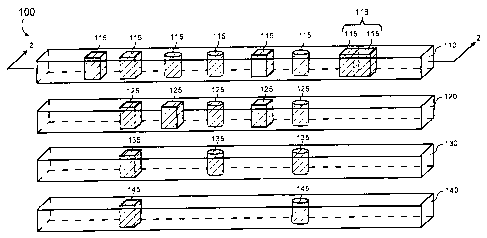
Referring to Fig. 1, a cross-sectional view of a
substrate 100 is shown which is useful for understanding the
5
CA 02561955 2006-10-02
WO 2005/099028 PCT/US2005/010300
present invention. The substrate 100 can include one or more
layers, for example layers 110, 120, 130, 140. Typical layer
thicknesses can be from 0.5 mils to 10 mils. The substrate
layers 110, 120, 130, 140 can be formed from any dielectric
material wherein vias can be formed. For example, the
substrate layers can be formed from ceramic material, such as
low temperature co-fired ceramic (LTCC) or high temperature
co-fired ceramic (HTCC). The substrate layers also can be
formed from fiberglass or epoxy insulator reinforced with
fiber, such as FR4. Moreover, polymers, such as polymide,
polyester, polypropylene or other polymer film can be used as
the dielectric. Still, the invention is not so limited and
many other dielectric materials can be used.
An example of LTCC material that can be used is 951
Green Tape''M, available The DuPont Company of Research Triangle
Park, NC 27709. The relative permittivity (er) of 951 Green
Taper" is approximately 7.8. Another LTCC material that can be
used is part number K2400 available from Ferro Corp. of
Cleveland, Ohio 44114. K2400 is available as a powder that
can be used to formulate LTCC tape. K2400 has a relative
permittivity (~r) of approximately 2400. Nonetheless, powders
having other permittivity values are available. In one
arrangement, the substrate 100 can comprise multiple substrate
layers having different permittivity. Accordingly, electric
field density can be different in different parts of the
substrate 100. Such an arrangement can provide further
control over the capacitance values of the embedded
capacitors.
One or more vias 115 can be formed within the first
substrate layer 110. Vias also can be formed within other
substrate layers as well. For example, vias 125 can be formed
in a second substrate layer 120, vias 135 can be formed in a
third substrate layer 130, and vias 145 can be formed in a
fourth substrate layer 140, and so on. Many techniques are
6
CA 02561955 2006-10-02
WO 2005/099028 PCT/US2005/010300
available for forming vias in a substrate layer. For example,
in some substrates, such as ceramic substrates, vias can be
formed by laser cutting holes through the substrate, drilling
holes through the substrate, or mechanically punching the
holes. In a preferred arrangement, the vias can be
mechanically punched as this allows the tolerance of the
cross-sectional area of each via to be tightly controlled.
For example, tolerances of ~ 0.1 mils can be maintained.
Further, if a substrate is used that is subject to shrinkage,
it is preferred that the substrate be preconditioned before
being used in a fabrication process in order to minimize
shrinkage after the vias have been formed. Such shrinkage can
cause the tolerance of the vias to vary. An exemplary
preconditioning process is discussed below.
The vias 115, 125, 135, 145 can be formed so that
each via has a same cross sectional profile, or the size of
each via 115 can be optimized to achieve a desired capacitance
value once the vias have been filled with a conductive
material. Vias also can be overlapped, or stepped, for
example to form a larger via 11~ with an increased cross
sectional area. Further, vias 115, 125, 135, 145 can be
formed to have any desired shape.
After the vias 115, 116, 125, 135, 145 have been
formed in the substrate layers 110, 120, 130, 140, the vias
2 5 can be filled with a conductive material 250, as shown in Fig.
2. The conductive material can be any suitably conductive
material. For example, a conventional thick film screen
printing material, such as that used in a standard emulsion
thick film process, can be used to fill the vias. For
instance, the conductive material can be a conductive paste.
One such conductive paste is part number CN 33-343 silver via
paste available from Ferro Corp. of Cleveland, Ohio 44114.
Nonetheless, the invention is not so limited and any suitable
conductive material that can be used to fill the vias can be
7
CA 02561955 2006-10-02
WO 2005/099028 PCT/US2005/010300
used. Once the vias have been filled with a suitable
conductive material, the substrate layers then can be baked to
dry the conductive material within the vias. For example, if
the substrate layers are LTCC, the substrate layers can be
dried at 120° C for 5 minutes.
Referring to Fig. 3, conductive layers then can be
deposited on the substrate layers, where required. The
conductive layers can provide electrical connections to the
electrodes. For example, a conductive layer 355 can be
deposited on substrate layer 110 and a conductive layer 360
can be deposited on substrate layer 140. Again, a
conventional thick film screen printing process can be used to
deposit conductive layers on the substrate layers and the
substrate layers can be baked to dry the conductive layers.
Once the conductive layers have been dried, the
substrate layers 110, 120, 130, 140 can be joined to form
substrate 400, as shown in Fig. 4. Notably, additional
substrate layers (not shown) also can be joined to substrate
layers 110, 120, 130, 140. The additional substrate layers
also can comprise vias and conductive layers. In a preferred
arrangement, conductor filled vias in the substrate layers
110, 120, 130, 140 which are opposingly disposed can be
aligned to form electrodes 465, electrodes 467 and electrodes
475, each of which can extend through multiple substrate
layers. Further, conductor filled vias not having associated
vias in other substrate layers can form electrodes 470.
Various methods can be used to join the substrate
layers. For example, the layers can be laminated together
using a variety of lamination methods. In one method using
ceramic substrate layers, the substrate layers can be stacked
and hydraulically pressed with heated platens. For instance,
a uniaxial lamination method can press the ceramic substrate
layers together at 3000 psi for 10 minutes using plates heated
8
CA 02561955 2006-10-02
WO 2005/099028 PCT/US2005/010300
to 70° C. The ceramic substrate layers can be rotated 180°
following the first 5 minutes.
In an isotatic lamination process, the ceramic
substrate layers can be vacuum sealed in a plastic bag and
then pressed using heated water. The time, temperature and
pressure can be the same as those used in the uniaxial
lamination process; however, rotation after 5 minutes is not
required. Once laminated, the structure can be fired inside a
kiln on a flat tile. For example, the ceramic substrate
layers can be baked between 200° C and 500° C for one hour and
a peak temperature between 850° and 900° can be applied for
greater than 15 minutes. After the firing process, post fire
operations can be performed on ~he ceramic substrate layers.
A temperature release tape, such as P/N 3195M,
available from Nitto Denko Co., Ltd. of Hong Kong, can be used
to facilitate stacking of substrate layers during the
lamination process. For example, the temperature release tape
can be applied to each substrate stack (or substrate substack
if more than one stack is used) to provide a solid base on
which thin tape then can be mounted. For instance, a first
piece of thin tape in the stack can be mounted to the
temperature release tape to begin the stack. Each subsequent
layer then can be laminated to that stack. The temperature
release tape can be released from the substrate layers during
the baking process. Using this process, correlating
conductive vias in adjacent substrate layers and substacks can
be electrically continuous.
In operation, electrodes 465, 467, 470 can be
capacitively coupled to electrodes 475 and conductive layer
360. For example, the conductive layer 360 can be grounded so
that the conductive layer 360 and electrodes 475 are grounded
conductors. When a voltage is applied to the conductive layer
355, electric fields can form between the electrodes 465, 467,
9
CA 02561955 2006-10-02
WO 2005/099028 PCT/US2005/010300
470 and the grounded conductors. The amount of capacitance
formed between the electrodes 4G5, 467, 470 and the grounded
conductors is primarily a function of the relative
permittivity of the substrate layers 110, 120, 130, 140, the
surface area of the electrodes 465, 470, and the proximity of
the surface of the electrodes to the grounded conductors.
Accordingly, the surface area of the electrodes, the
permittivity of the substrate layers 110, 120, 130, 140, and
the distance between the substrates and the grounded
conductors can be selected to achieve a desired capacitance
value. For instance, the dimensions of electrodes 465 can be
precisely selected for a desired capacitance value using
substrate layers having a particular permittivity.
There may be some capacitive coupling between
electrodes 465 and electrodes 475 due to the area of the
parallel surfaces and the proximity of the electrodes 465 to
the electrodes 475. However, this capacitive coupling is
relatively insignificant at typical dimensions and via
orientations. Further, the permittivity of the individual
substrate layers 110, 120, 130 can be selected to reduce or
increase capacitive coupling between the electrodes 465 and
electrodes 475 as desired.
A significant portion of the capacitive coupling
associated with electrode 467 can be determined by the
capacitive coupling between the electrode 467 and the
conductive layer 360 due to the proximity of the electrode 467
to the conductive layer 360. The thickness of the substrate
layer 140 can be selected to achieve a desired distance
between the electrode 467 and the conductive layer 360.
Still, there will be capacitive coupling between the electrode
467 and electrodes 475. At this point it should be noted that
the embodiment shown in Fig. 4 is shown for exemplary purposes
and that the invention is not so limited. Importantly, any
number of electrodes can be provided. Moreover, the grounded
CA 02561955 2006-10-02
WO 2005/099028 PCT/US2005/010300
conductors need not include both electrodes 475 and conductive
layer 360. For instance, one arrangement can include the
conductive layer 360 as the only grounded conductor.
Referring to Fig. 5, an exemplary substrate is shown
which includes electrodes 580. Low values of capacitance can
be provided between the electrodes 580 and grounded conductors
595, for example values less th;~n 50 pF. The capacitance
values depend from the surface area of the electrodes, the
permittivity of the substrate, and the distance between the
electrodes and the grounded conductors. Further, an electrode
585 which is electrically coupled to a conductive layer 590
can be provided. Such a configuration can be used to provide
a high capacitance value, for instance in excess of 10 nF,
between the conductive layer 590 and the grounded conductors
595. In the arrangement shown, the conductive layer 590 can
be disposed between grounded conductive layers 597, 598. Such
an arrangement can result in a larger capacitance value in
comparison to an instance where only a single grounded
conductive layer is provided. In particular, the use of
multiple conductive layers 597, 598 increases the surface area
of the grounded conductors, thereby increasing the capacitive
coupling. The surface area of the conductive layers can be
selected to provide a desired capacitance value for a given
substrate layer permittivity and thickness.
A method 600 of manufacturing embedded capacitors in
a substrate is shown in Fig. 6. Referring to step 605,
substrate layers can be preconditioned before being used in a
fabrication process. For example, if the ceramic substrate
material is used, the substrate can be baked at an appropriate
temperature for a specified period of time or left to stand in
a nitrogen dry box for a specified period of time. Common
preconditioning cycles for ceramic material are 120° C for 20-
30 minutes or 24 hours in a nitrogen dry box. Both
11
CA 02561955 2006-10-02
WO 2005/099028 PCT/US2005/010300
preconditioning process are well known in the art of ceramic
substrates.
Referring to step 610, one or more vias, or bores,
can be created in each of the substrate layers that are to
incorporate vias. As previously noted many techniques are
available for forming bores in a substrate layer, such as
mechanically punching or laser cutting holes into the
substrate layer. In the preferred arrangement, the vias are
formed after the preconditioning of the substrate layers.
However, if a particular dielectric does not exhibit much
shrinkage due to the baking steps described below, the
preconditioning step may not be required.
The vias can then be filled with a conductive
material as shown in step 615. For example, as noted, a
conventional thick film screen printing material can be used
to deposit conductive material within the vias. The
conductive material then can be dried as shown in step 620.
For example, if the substrate layers are LTCC, the LTCC can be
baked at 120° C for 5 minutes.
Proceeding to step 625, conductive layers then can
be deposited on the substrate layers. For example, a
conventional thick film screen printing process, such as a
standard thick film process, can be used to deposit conductive
layers on the desired substrate layers. The substrate
layers) then can be baked to dry the conductive traces, as
shown in step 630.
Referring to step 635, the substrate layers can be
laminated together after appropriate preconditioning and
drying of circuit traces. A variety of techniques for
laminating substrates are known to those skilled in the art of
substrate manufacturing, as previously discussed. Once the
substrate layers have been laminated, the laminated substrate
structure then can be sintered, as shown in step 640. For
example, in the case that the substrate is LTCC, the first and
12
CA 02561955 2006-10-02
WO 2005/099028 PCT/US2005/010300
second substrate layer combination can be sintered at
approximately 850° C to 900° C for 15 minutes.
13