Note: Descriptions are shown in the official language in which they were submitted.
CA 02562077 2006-10-05
WO 2005/109647 PCT/US2005/008549
ADJUSTABLE FREQUENCY DELAY-LOCKED LOOP
FIELD OF THE INVENTION
The present invention relates generally to direct digital frequency synthesis
and more specifically to a delay-locked loop configuration for reducing
spurious
output signals.
BACKGROUND OF THE INVENTION
A number of devices, for instance mobile applications such as portable
devices, require the use of a frequency synthesizer for operation. One such
frequency
synthesizer includes a digital-to-phase converter having a digital delay-
locked loop
(DLL). FIG. 1 illustrates a schematic diagram of a prior art DLL 10
configuration for
generating an output signal 72 at a desired frequency Fo"t. DLL 10 comprises a
fixed
frequency synthesizer 20 for generating a clock signal 22 having a frequency
of F~lk.
DLL 10 further comprises: a delay line 30 having N number of adjustable delay
elements D1 through DN; a phase detector 40, a charge pump 50 and a loop
filter 60,
which make up a stabilization circuit for DLL 10; a selection circuit 70 that
may be,
for instance, a multiplexer (also referred to herein as a "MUX"); and a
digital control
device 90.
In operation, delay line 30 receives the clock signal 22 into an input and
then
generates a set of time delayed clock signals at a plurality of outputs. The
time delays
are generated by delay elements D 1 through DN, which are connected in cascade
and
which may be, for instance, inverter gates, transmission line gates, and the
like,
depending upon a desired DLL implementation. Moreover, an overall time delay
between a signal at first point on the delay line, which is typically an input
of the first
delay element D1, and a signal at a second point on the delay line, which is
typically
the output of the Nth delay element DN, is controlled by a bias voltage Vtune
input into
delay line 30. This overall delay may be, for instance, a wavelength (i.e.,
360
degrees) which is 1 period of clock signal 22, a half wavelength (i.e., 180
degrees)
which is %a period of clock signal 22, or whatever delay is required for a
particular
application. Ideally, each delay element will replicate the input waveform,
with a
time delay, at the delay element output that is equal to the total delay from
the input of
CA 02562077 2006-10-05
WO 2005/109647 PCT/US2005/008549
delay element D1 through the output of delay element DN divided by the total
number
of delay elements (i.e., N).
Each delay element D1-DN has an output tap T1-TN, respectively, which is
connected to an input of MUX 70. In addition, a tap TO is connected between
the
input of the delay element Dl and an input of MLTX 70 in order to supply the
clock
signal 22 thereto. Each delay element D1-DN delays the propagation of the
clock
signal 22 and outputs on its corresponding output tap T1-TN, respectively, a
corresponding phase shifted clock signal. Accordingly, the number N of phase-
shifted clock signals output by delay elements D1-DN are supplied via output
taps
T1-TN to the inputs of MUX 70 along with the clock signal 22 output on tap T0.
To ensure stability during operation, DLL 10 includes phase detector 40 that
is
typically connected to receive the clock signal 22 from synthesizer 20 and a
phase
shifted clock signal from delay line 30, which in this instance is the signal
at the
output of delay element DN. Phase detector 40 compares the phase difference
between the clock signal 22 and the phase shifted clock signal to a
predetermined
desired phase shift and outputs to the charge pump an error signal that is a
function of
the result of this comparison. Those of ordinary skill in the art should
realize that
phase detector 40 could be configured for comparing the phase difference
between the
signals at any two points on the delay line to the predetermined desired phase
shift
acid outputting the corresponding error signal.
The charge pump 50 deposits a corresponding charge on the loop filter 60,
which in turn converts the error signal into a DLL tuning signal which is
supplied to
delay line 30 to adjust the bias voltage Vtune in a manner that maintains the
phase
relationship between the phase shifted clock signal and the clock signal 22
during
operation of DLL 10, i.e., until the total delay through the delay line is the
desired
delay. Once DLL 10 has stabilized, MUX 70 operates in a conventional way under
the control of digital control 90 to connect, one at a time, a sequence of
phase-shifted
clock signals at taps TO-TN to corresponding outputs of MUX 70 to provide an
output
signal at the desired output frequency Fo"t. The digital control device 90 is
typically a
tap selection controller that comprises two accumulators, one to determine
when to
connect a tap to an output terminal and another to determine which tap to
connect.
This tap selection sequence is typically based on Fo"t, F~~k and N.
CA 02562077 2006-10-05
WO 2005/109647 PCT/US2005/008549
There are a finite number of transitions that can be selected from the delay
line
30 to create an output signal at a desired frequency. The possible error
associated
with the selection of a given tap to create the output signal causes a
quantization
effect which creates spurious signal outputs (spurious being undesired
spectral
components). The effect can be minimal if the selected frequency and the clock
signal frequency happen to fall on certain values. However, in general the
spurious
free dynamic range will be limited by the quantization effect of the taps.
FIG. 2 illustrates the misalignment between the desired output signal
transitions and those of the actual output signal 72 generated in DLL 10. This
misalignment is caused by a round off error which results in spurious signals
generated at the output 72 of MUX 70. Let us assume that delay line 30
includes four
delay elements D1 through D4. FIG. 2, accordingly, illustrates clock signal 22
(i.e.
waveform 210 having no time delay or a zero phase shift) and three
corresponding
time delayed or phase-shifted clock signals (i.e., waveforms 220, 230 and 240)
output
therefrom. Assuming a total delay from the input of D 1 to the output of D4 is
one
wavelength, the waveform output from D4 would be equivalent to wavefonn 210.
As
FIG. 2 illustrates, each waveform ideally has the same frequency as the clock
signal
22 (i.e., F~tk) but may have a different delay in time. Moreover, in this
illustration
from a time tn to a time t4, twenty-two edge transition times or delay times
(i.e., d0
through d21) are generated from which MUX 70 can select to generate the
desired
output waveform 260.
Given the number of taps, the frequency of the clock signal 22, and the
desired
output frequency, the potential delay times can be calculated by digital
control device
90 and selected by MUX 70 to generate a corresponding output signal 250. This
relationship may, for instance, be represented by the following equation:
Fcuc=(M'~fout)~N~ forlVhN (1)
where F~~k is the frequency of the clock signal 22, Foot is the desired output
frequency,
N is the number of taps and M represents the delays that would be required to
generate the desired output signal waveform 260. This relationship may,
alternatively, be represented by the following equation:
CA 02562077 2006-10-05
WO 2005/109647 PCT/US2005/008549
4
T°ut=(M*T~lx)~N, for lVnN (2)
where M and N are,the same as in equation (1), T~lx is the period of F~lx,
Tout is the
period of F°"t and T~~x/N represents a delay caused by a single delay
element. Ideally,
to generate an output signal having no spurious signals, M would equal an
integer
number of delays (i.e., delays=T~lx/N). However, typically this is not the
case.
Generally, M is a non-integer multiple of delays and taps are then selected
above and
below the desired multiple of delays thereby generating a waveform 250 that
has the
desired output period on average.
Referring again to FIG. 2, assume that M=5.4, for example, for a given
T°°t,
T~~x and N. In this case, the edge transition times for the desired output
waveform 260
would be at 5.4 delays, 10.8 delays, 16.2 delays, 21.6 delays, etc. To
generate the
closest waveform 250 to the desired waveform 260, the desired delays would be
rounded to the nearest integer multiple of delays, e.g., 5 delays (d5), 11
delays (dl 1),
16 delays (d16), 22 delays (d22), etc. This round-off error or quantization
effect
causes the spurious outputs. Thus, the farther the actual selected delay is
from the
desired delay (i.e., the larger the round-off error) the larger the
corresponding
spurious signal being generated at the output.
One way known in the art of improving the spurious performance or reducing
the spurious level relative to the desired output signal is to increase the
number of taps
in the delay line 30. This would result in the actual selected delays being
closer to the
desired delays (i.e., smaller round-off errors) and resulting smaller spurious
signals
being generated at the output. However, a limitation of this solution is that
each tap
that is added degrades the noise performance of the DLL and increases the
complexity
of the tap selection circuitry 70. In addition, although theoretically an
infinite number
of taps may be added, practically the number of taps possible is limited as
present day
technologies will not support the complex level of circuitry needed if the
number of
taps increases beyond a certain point, e.g., where the tap selection network
switching
delay approaches a 10% fraction of T~~x.
Another method known in the art for improving the spurious performance is
the use of dither. However, in general, while the use of dither reduces the
spurious
CA 02562077 2006-10-05
WO 2005/109647 PCT/US2005/008549
energy at specific frequencies, it also essentially spreads this energy over a
broader
bandwidth thereby creating a floor of quantization noise. Thus, to decrease
the
spurious signal, and accordingly this wide band noise, to an acceptable level
in certain
applications, an unrealizable number of taps in addition to the dither would
be
required.
Thus, there exists a need for a DLL configuration that minimizes the level of
spurious signals without requiring more taps to be added to the DLL and that
further
does not require the use of dither with its associated wide band noise.
BRIEF DESCRIPTION OF THE FIGURES
A preferred embodiment of the invention is now described, by way of example
only, with reference to the accompanying figures in which:
FIG. 1 illustrates a simple block diagram of a prior art delay-locked loop
configuration;
FIG. 2 illustrates the misalignment between the desired output signal and the
output signal generated by the delay-locked loop configuration of FIG. 1;
FIG. 3 illustrates a simple block diagram a of a delay-locked loop
configuration in accordance with an embodiment of the present invention;
FIG. 4 illustrates a flow diagram of a method for generating an output signal
in a delay-locked loop in accordance with an embodiment of the present
invention;
FIG. 5 illustrates a simple block diagram of an embodiment of an adjustment
and tap selection controller in accordance with the present invention;
FIG. 6 illustrates a simple block diagram of a delay-locked loop configuration
in accordance with another embodiment of the present invention;
FIG. 7 illustrates the alignment of the desired output signal when spurious
signals are reduced in accordance with the present invention;
FIG. S illustrates a simple block diagram of another embodiment of an
adjustment and tap selection controller in accordance with the present
invention; and
FIG. 9 illustrates a simple block diagram a of delay-locked loop configuration
in accordance with another embodiment of the present invention.
CA 02562077 2006-10-05
WO 2005/109647 PCT/US2005/008549
DETAILED DESCRIPTION OF THE INVENTION
While this invention is susceptible of embodiments in many different forms,
there are shown in the figures and will herein be described in detail specific
embodiments, with the understanding that the present disclosure is to be
considered as
an example of the principles of the invention and not intended to limit the
invention to
the specific embodiments shown and described. Further, the terms and words
used
herein are not to be considered limiting, but rather merely descriptive. It
will also be
appreciated that for simplicity and clarity of illustration, elements shown in
the
figures have not necessarily been drawn to scale. For example, the dimensions
of
some of the elements are exaggerated relative to each other. Further, where
considered appropriate, reference numerals have been repeated among the
figures to
indicate corresponding elements.
The present invention uses an adjustable frequency source to force the period
of the output signal to be an integer number M of delays (T~lk/I~, referring
to equation
(2). This results in the quantized edge transition times of the actual output
signal
corresponding with the desired edge transition times to reduce and ideally
eliminate
spurious signals in the output.
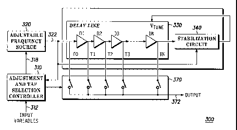
FIG. 3 illustrates a simple block diagram a of delay-locked loop configuration
300 in accordance with an embodiment of the present invention. DLL 300
comprises:
an adjustable frequency source 320 for generating a clock signal 322 having an
adjustable frequency of F~l~,ariable that is based upon at least one frequency
adjustment
value 31~; an adjustment and tap selection controller 310 having an input for
receiving one or more input variables 312 that includes an indication of the
desired
output frequency Fo"t, and may also include other variables such as, for
instance, N if
it has not been preprogrammed or preset into controller 310 and a range of
possible
frequency values for F~l~,ariable; a delay line 330 having N number of
adjustable delay
elements D1 through DN connected in cascade and having respective output taps
TO
through TN, and elements Dl-DN further having an overall delay of L between
two
points on the delay line (typically but not necessarily between signal 322 at
the input
of Dl and the signal at the output of DN) that for purposes of simplifying the
following discussion will equal to one, which corresponds to one wavelength,
in this
example of clock signal 322; and a selection circuit 370 that may be, for
instance, a
CA 02562077 2006-10-05
WO 2005/109647 PCT/US2005/008549
multiplexer (also referred to herein as a "MUX") that includes inputs coupled
to taps
TO through TN.
DLL 300 may also optionally include a stabilization circuit 340 for
stabilizing
the delay line to substantially a predetermined desired phase sluft between a
signal at
a first point and a signal at a second point on the delay line, which in this
illustration
is from the input of D 1 to the output of DN. The delay line is ideally
stabilized to
within a range of the desired phase shift that corresponds to an acceptable
spurious
level at the output depending on a particular application. Stabilization
circuit 340
may include, for instance, a phase detector for comparing the phase difference
between the signals at the first and second points on the delay line to the
predetermined desired phase shift and providing an error signal indicative of
the result
of the comparison, wherein the error signal is used (typically after having
been
smoothed, for instance, using a conventional filtering technique) to adjust
the delay
line to the desired predetermined delay. Stabilization 340 may further include
at least
one of a charge pump and a loop filter as illustrated in FIG. 1 and whose
operation is
well known in the art and described above.
Delay line 330 and MUX 370 may be implemented using conventional
elements such as those described above by reference to FIG. 1. Thus, their
operation
is well known by those skilled in the art as described above by reference to
FIG. l, the
details of which will not be repeated here for the sake of brevity. However
controller
310 and adjustable frequency source 320 are configured in accordance with the'
present invention, as described in detail below, to enable F~~k,,a,;able to be
programmed
or set to eliminate or reduce spurious signals at the output 372.
FIG. 4 illustrates a flow diagram of a method in accordance with an
embodiment of the present invention for use in a DLL (e.g., DLL 300 in FIG. 3)
for
generating an output signal 372. In accordance with this method, at least one
input
value corresponding to the desired output signal frequency Four is received
(400) into
input 312 of the adjustment and tap selection controller 310. This value may,
for
instance, result from a command from the device incorporating the DLL to
operate at
a certain frequency and is generally a digital value corresponding to Fout.
Upon
receipt of this digital value, the adjustment and tap selection controller 310
determines
(410) an F~»,a,;able that would generate an output signal having the same or
CA 02562077 2006-10-05
WO 2005/109647 PCT/US2005/008549
substantially the same frequency as the desired Four, to a typical frequency
tolerance of
lppm to l Oppm (parts per million). In other words an output signal would be
generated that eliminates or at least minimizes quantization effect spurious
signals at
the output to the extent possible, given, for instance, any other limitations
in the
circuit such as, for instance, a mismatch in the delay elements or other such
limitations known in the art. F~»,a,;abie may be computed based upon, for
instance,
iteratively applying equation (1) and (2) to determine an F~»,a,;abl~out ratio
that
corresponds to the ratio of M/N, thereby forcing the output period to be an
integer
number M of delays.
For the computed F~ma,;abie and M, the adjustment and tap selection controller
310 may determine (420), in accordance with the present invention, a sequence
of tap
selection values and corresponding phase-shifted clock signals to be selected
one at a
time for generating the desired output signal. This sequence of tap selection
values
may include all of the available tap selection values corresponding to the
available
phase-shifted clock signals or alternatively may include only a portion
thereof. The
adjustable frequency source 320 may then adjust the clock signal 322 (430),
under the
control or direction of the adjustment and tap selection controller 310, such
that signal
322 has substantially the frequency F~I~,a,;able that was computed by
controller 310.
This causes delay line 330 to be locked (440) to the desired phase shift,
e.g., the
desired wavelengths L of clock signal 322. When the delay line is locked, the
tap
selections determined by the adjustment and tap selection controller 310 can
be
applied (450) by MUX 370 to generate an output signal 372 having substantially
the
desired output frequency, i.e., wherein the frequency of waveform 250 is
substantially
equal to the frequency of waveform 260.
In this case, the delay line is locked to one wavelength such that L=1.
However, those of ordinary skill in the art will realize that L may be set to
another
value such that the delay line is locked to, for instance, a half wavelength
or a quarter-
wavelength. In the case where L is not equal to one, a data bus line may be
connected
from the controller 310 to the delay line or, for instance, to a phase
detector in the
stabilization circuit 340 for adjusting the delay line to the desired phase
shift.
Following is a detailed description of embodiments of the adjustment and tap
selection controller 310 and the adjustable frequency source 320 that would
enable the
CA 02562077 2006-10-05
WO 2005/109647 PCT/US2005/008549
9
method of FIG. 4 to be implemented in a DLL configuration such as DLL 300. In
accordance with the present invention, generation of the programmable clock
signal
322 may, for instance, be implemented using a frequency synthesizer such as,
for
instance, a conventional fractional-N phase-locked loop having at least one
input
variable that is based on F~t~,a~able and that is determined by the adjustment
and tap
selection controller 310. Adjustable frequency source 320 is hereinafter
interchangeably referred to as adjustable frequency synthesizer (320) but
without any
intention of limiting the frequency source (320) to the specific frequency
synthesizer
implementation.
The signal output 322 from synthesizer 320 will typically have a frequency
Fclx~ariabie that may vary from a minimum frequency Fm;" to a maximum
frequency
F",~. To determine this variance, let us assume for the moment that
F~~k,,a,.;able is fixed
similar to the frequency F~lk of signal 22 of FIG. 1, wherein,
h-'min F~xee -OF1, and (3)
Fm~ f'~Xea +~F2, (4)
where F~;Xea is assumed fixed frequency, and where generally OFl=tlF2.
The following analysis explains how much synthesizer 320 is ideally
configured to vary. Consider equation (5) for a system that uses a fixed
frequency
synthesizer for a delay-locked loop as denoted by F~;Xea as shown below:
MxF
F,-rxed =
Using this relationship:
M=~''f~e~XN
Fo"t
CA 02562077 2006-10-05
WO 2005/109647 PCT/US2005/008549
However, for some desired output frequencies Fouc and a given Ffxea~ there
will be
frequencies that cannot be satisfied by using integer values for M. This is
shown
below by adding the error s to the integer M:
5 M+~= Ff'~edxN ( )
Fout
In order to insure that all cases can be satisfied for a given frequency band,
a
frequency source is used that can be varied over a limited frequency range.
The
frequency required to eliminate the error of s introduced above can be found
by:
- (M ~ s) x Fauc M x Four + s x Four (8)
Fclkvariable = Ffixed -~- L~F - -
N N N
10 In this scenario, the frequency is either increased or decreased to reach
the nearest
integer M. Therefore, s<I/2.
The amount of variability needed for the frequency source (not including what
is needed for temperature or supply variation) is as follows:
s x ~r'out
N ° ~ ~ (9)
fixed M x Fout M
N
The worst case would be for the lowest M. In the case of a 32 tap delay line
(N=32),
lVlr?N, so the worst case M would be 33 (assuming that you would not want to
regenerate the reference frequency). Therefore, the maximum variation would
be:
~ ~ _ ~ 12' _ ~0.0152 (10)
M 33
CA 02562077 2006-10-05
WO 2005/109647 PCT/US2005/008549
11
or +/1.52%, which would equate to a total variation of 3.04%. This is a
limited
freuqency range that is very small compared to the available frequency
variablily of
the signal at ouput 372, wick can span at least one decade of frequency.
This relationship can be extended to find the worst case variation in the
adjustable synthesizer for a delay line of any number of elements. As noted
above,
the worst case would be when M is one more than the number of taps and when
s<'/2.
Therefore, the worst case variation required to optimize the spurious
performance for an N tap delay line would be:
1
~ (wo~stcase) _ ~ - 1 (11)
I'f~ed N+1 2N+2
This means that for a 64 tap delay line (note that the number of delay
elements
or taps in a delay line does not necessarily need to be a power of 2) the
worst case
variation required of the variable frequency source is +/-.8% or a total
variation of
1.6%. This is half the total variation needed as compared to that needed for a
32 tap
line, which as determiend above required a 3.04% total variation.
FIG. 5 illustrates a block diagram of an embodiment of an adjustment and tap
selection controller 310 in accordance with the present invention shown
coupled to
the adjustable frequency source 320. Tap selection controller 310 includes a
processor 316 that is configured for processing an algorthm in hardware or one
that is
stored in a memory as softwaxe for determining F°»,ar;able for a
desired frequency F°°t
and for outputing at least one frequency adjustment value 318 to frequency
source
320 such that it adjusts the frequency of clock signal 322 to substantially
F°»,a~;avle.
Processing device 316 further determines a sequence of selection values, C~,
corresponding to a sequence of phase-shifted clock signals and outputs to the
MUX
370 the sequence of selection values such that MUX 370 selects the
corresponding
sequence of phase-shifted clock signals one at a time to generate output
signal 372.
Processor 316 is ideally a digital signal processor.
CA 02562077 2006-10-05
WO 2005/109647 PCT/US2005/008549
12
Adjustment and tap selection controller 310 may also, optionally, include a
memory element 314 for storing the sequence of selection values and for
outputting
the sequence to MUX 370, and a sequencer 311 for controlling the timing of the
output of the sequence of selection values from the memory element 314.
Sequencer
311 may be, for instance, any suitable counter for controlling the timing of
the output
of the sequence of selection values based upon the clock signal 322, as
illustrated in
FIG. 5, and memory element 314 may be, for instance, a read only memory.
With the elimination of quantization effect in the digital-to-phase converter
process, a predetermined sequence of tap selections can be managed with the
reduced
digital processing architecture of a processor or a processor in combination
with
sequencer 31 l and memory element 314 as illustrated in FIG. 5. Accordingly,
the
digital processing can be reduced to counting the input clock cycles and
sequencing
through a predetermined set of tap selection values C~. This can be reduced to
a
simple operation of incrementing through a set of memory addresses containing
the
corresponding tap selection values, where the address increment also
corresponds to a
given clock frequency F~I~a~able. A more detailed explanation of the operation
of
controller 310 follows.
Processor 316 receives as inputs the programming variables 312 that are
necessary to calculate the programming values for the adjustable frequency
synthesizer 320, the memory 314, and counter 311. The input variables would be
those that are necessary to solve equation 1. For example, the device into
which the
invention is incorporated, such as a portable communications device, might
program
into processor 316 the desired output frequency (Four) the number of taps (N)
that are
present in the delay line (330 of Figure 3), and the frequency range
(Fmin~Fc~x~Fmax )
of the adjustable frequency synthesizer 320. Based on these inputs, the
processor 316
would use equation 1 to solve for M or a range of M values that would satisfy
the
equation, wherein M is an integer so as to provide the most reduction in
spurious
outputs. An M value would be selected from the solution set and would then be
used
to calculate an F~»,ambte value that would correspond with the desired output
frequency (Four), the M value calculated above, and the given number of taps
used in
the delay line.
CA 02562077 2006-10-05
WO 2005/109647 PCT/US2005/008549
13
Once the desired F~l~,a,;abte is calculated, the programming variables 318
necessary for realizing the required clock input to the delay line 330 would
be written
to the adjustable frequency synthesizer 320. The processor 316 could then
calculate
the tap selection sequence needed to create the desired output frequency
(Fo"t) and
S generate the corresponding tap selection values to load into memory 314.
These tap
selection values are referred to in Figure 5 as C~, where j corresponds with
the address
of the memory location in which the tap selection value is stored. For the
sake of
simplicity, C~ will be a tap address (ie. C~=0 would correspond with tap 0,
C~=1 would
correspond with tap l, etc.). However, in the actual implementation the tap
selection
values written to memory might be a bit sequence, each bit corresponding with
a tap
selector in MUX 370 (for example, for a 4 element delay line a value of 1000
in
memory 314 would connect tap 0 to the output in MUX 370, a value of 0100 would
connect tap 1 with the output, etc.).
For the embodiment of Figure 5, the contents of a memory address j is output
to MUX 370 for every cycle of the adjustable frequency synthesizer output
clock 322.
Depending on the ratio of the clock frequency to the desired output frequency
(Fclkvariable~out)~ ~ output transition may not be needed for a given period
of the clock
322. Therefore, some memory addresses will contain a null value so as not to
enable
a tap during that particular clock cycle. Given this, the tap selection values
that are
stored in memory 314 are calculated as follows:
1. Designate the sequence to begin with one of the taps. For simplicity, the
sequence may begin with the first tap, To. Therefore, the first C~ value to be
stored in memory would the address of To, or Co = 0.
2. Determine whether or not a tap is required in the next clock cycle using
the
following equation:
M+~'
x = T~uhc N ' -1 (12)
.l
where x~ determines the number of clock cycles following the cycle
corresponding to C~ that do not contain an output cycle. For each skipped
CA 02562077 2006-10-05
WO 2005/109647 PCT/US2005/008549
14
clock cycle, a null value is programmed into the corresponding address of
memory 314. Note here that the Trunc operation removes the fractional
portion of the number resulting from the expression in parenthesis. For
M+C'
example, if N ' = 3.9 then Trunc(3.9) would evaluate to the integer value
of 3.
3. Once the required number of skipped clock cycles is determined and
programmed, the tap to be selected in the next clock cycle is calculated using
the following:
C';+1= Mod L~~';vaua + Mod (M, N) ~, N
(13)
where Mod refers to the Modulus function as defined below: Mod[n,m] = n
modulus m = integer remainder of n/m. For example, Mod[33,32]=1,
Mod[32,32]=0, Mod[17,8]=1. Note that in equation (13) above, the Cj~alid
would refer to the last valid Cj value (not including a null value).
Therefore, if
when calculating the next tap selection value the current value in address j
is
null, the previous value for C~ would be used (ie., C~_1). If C~_1 is a null
value,
then the prior value would be used (C~_2). This process continues until a
valid
tap selection value is obtained (C~~~l,a) and this value is used.
4. Steps 2 and 3 are repeated until the required number of tap selection
values are
derived. Note that the maximum number of taps in a sequence is M
(including null values representing skipped clock cycles). However, if M is a
multiple of Mod[M,N], then the tap sequence can be reduced to
~N/(Mod[M,N])) plus the number of skipped clock cycles.
CA 02562077 2006-10-05
WO 2005/109647 PCT/US2005/008549
As an example, consider a 4 tap delay line (N=4) and a value of M of 5, which
means that M/N = Sl4 =1.25, and Mod[M,N] is 1. Therefore, the tap addresses
(C~) could be calculated as shown in the following table:
j C j+1 Xj
0 0 C';+1=Mod[{0+Mod(5,4)},4]=Mod[1,4]=1 CTruncCS+Ol l _1=0
JJ4
1 1 ~';+i=Mod[{1+Mod(5,4)},4]=Mod[2,4]=2 ~Zy.ujzc~5+111 _1=0
JJ4
2 2 C';+1=Mod[{2+Mod(5,4)},4]=Mod[3,4]=3 ~~,j,u~c~5+211 _1=0
JJ4
3 3 null (x3=1) S+3 11
~Tj~~C _1=1
JJ4
4 null C';+1=Md[{3+Mod(5,4)},4]=Md[4,4]=0 (X~
not
calculated
for
(use last valid C~ which was skipped
C3=3) clock
cycles)
0 0 1 0
(repeat)
Processor 316 controls counter 311 through control line 313 in order to
program the counter for the calculated number of addresses loaded into memory
314.
Counter 311 is then driven by the adjustable frequency synthesizer output 322
so as to
count cycles of the clock signal that is applied to the input of delay line
330 for
10 synchronization of the delay line with the tap selection process. Counter
311, thus,
provides control to memory 314 to determine which memory location is actively
being read by MUX 370.
CA 02562077 2006-10-05
WO 2005/109647 PCT/US2005/008549
16
Therefore, once the adjustable frequency synthesizer 320 has reached the
programmed frequency F~»a,;able determined by controller 310 and the memory
314
and counter 311 have been loaded and configured for the desired output
frequency
(Fout)~ the counter 311 runs and steps through the locations in memory 314.
The
memory 314 in turn outputs the tap selection values to the MUX 370 at the
proper
time in order to multiplex the delayed clock signal to the output so as to
form the
desired output signal.
FIG. 6 illustrates a simple block diagram of a delay-locked loop configuration
in accordance with an embodiment of the present invention showing an expanded
controller 310 configuration. FIG. 6 includes each of the elements of the
embodiment
illustrated in FIG. 3, the details of which will not be repeated here for the
salve of
brevity. FIG. 6 further includes the expanded illustration of adjustment and
tap
selection controller 310 that is shown in FIG. 5, the details also of which
will not be
repeated here for the sake of brevity. However, what can be further seen by
the
embodiment in FIG. 3 is the connectivity of the outputs from controller 310 to
the
adjustable frequency synthesizer 320 and MUX 370. Specifically, the adjustable
frequency programming values) 318 are input into synthesizer 320 to program it
for
generating the clock signal 322 having the frequency F~l~,ariable determined
by
controller 310. In addition, the tap selection values C~ are coupled to the
MUX 370
for controlling the MUX to select the correct taps in the correct sequence and
with the
correct timing in order to generate the output signal 372 having the desired
output
frequency F~"t.
FIG. 7 illustrates the alignment of the desired output signal when spurious
signals are reduced in accordance with the present invention. Let us assume
that
delay line 330 includes four delay elements Dl through D4. FIG. 7,
accordingly,
illustrates clock signal 322 (i.e., waveform 710 having no delay or a zero
phase shift)
and three corresponding time delayed or phase-shifted clock signals (i.e.,
waveforms
720, 730 and 740) output therefrom. Assuming a total delay from D1 to D4 of
one
wavelength, the waveform output from D4 would be equivalent to waveform 710.
As
FIG. 7 illustrates, each waveform ideally has the same frequency but a
different delay
in time. Moreover, in this illustration from a time to to a time t~, twenty-
one edge
CA 02562077 2006-10-05
WO 2005/109647 PCT/US2005/008549
17
transition times or delay times (i.e., d0 through d20) are generated from
which MUX
370 can select to generate the desired output waveform 760. Assume that the
present
invention forces M=5, for example, for a given Tout, T~lk and N. In this case,
the edge
transition times for the desired output waveform 760 would be at 5 delays, 10
delays,
15 delays, 20 delays, etc., which are each an integer multiple of delays. Thus
controller 310 could direct MUX 370 to selects delays d5, d10, d15, d20, etc.
to
generate a waveform 750 that has the desired frequency.
FIG. 8 illustrates a simple block diagram of another embodiment of an
adjustment and tap selection controller 310 in accordance with the present
invention.
FIG. 8 includes each of the elements of the embodiment illustrated in FIG. 5,
the
details of which will not be repeated here for the sake of brevity. FIG. 8
further
includes a second memory element 315, which is ideally identical to RAM memory
element 314 for storing a second set of tap selection values, e.g., Cq, that
may be used
to generate a second output signal having substantially the same frequency as
signal
372 but is shifted in phase. Thus, the same process that was outlined above to
derive
the C~ tap selection values corresponding with the embodiment of Fig. 5 could
be used
to derive the C~ tap selection values for the embodiment of Fig. 8. In
addition, the Cq
values could be determined by shifting the C~ values by an amount that
corresponds to
the shift in phase between the two signals.
Those of ordinary skill in the art will realize that controller 310 may be
implemented as a processor, alone, having the same functionality as the stand-
alone
processor described above by reference to FIG. 5, but having the additional
functionality of determining a second sequence of selection values, Cq,
corresponding
to a second sequence of phase-shifted clock signals for generating the second
output
signal. Those of ordinary skill in the art will further realize that
controller 310 may
contain additional memory elements storing corresponding tap selection values
for
generating additional output signals having essentially the same frequency but
shifted
in phase from output signal 372. Moreover, although memory elements 314 and
315
are shown, for illustrative purposes, as separate boxes, this is not meant to
imply that
they must be separate elements. For example, a single memory device may be
used,
such as a single random access memory, for accomplishing the functionality of
these
CA 02562077 2006-10-05
WO 2005/109647 PCT/US2005/008549
18
memory elements. The number of additional output signals is limited by the
loading
restrictions on the delay line network.
In accordance with the embodiment of controller 310 illustrated in FIG. 8, a
common DLL system may be shared, for instance, for the generation of a set of
quadrature signals, wherein the two output signals generated differ in phase
by
substantially ninety degrees. Quadrature signals are a set of phase coherent
signals
used in image rejection frequency translation signal processing found, for
example, in
wireless communications equipment and thereby associated with wireless signal
processing. Quadrature may be defined, in this instance, as two signals being
offset
by a time value equal to 1/(4*Fo"t). Accordingly, tap selection values, Cq,
may be
determined by the following equation:
~'q = Mod ~'~ + ~ , N
(14)
wherein the Cq tap selection values axe generated by shifting the C~ values by
M/4.
The following example illustrates the process of calculating the tap selection
values for the above quadrature embodiment. Consider a delay locked loop
containing a delay line 330 having 8 taps (N = 8). The desired ratio of
Fclk/Fout is
1.5, so that the M of this example would be 12. The C~ tap selection values
can be
calculated using equations 12 and 13 above, and the Cq tap selection values
can be
calculated using equation 14 above. In this example, the Cg tap selection
values are
determined by shifting C~ by M/4=12/4=3. The table below illustrates the
calculated
C~ and Cq tap selection values:
Cj Cq Cj+1 xj
0 0 3 ~'~+~=Mod[{0+Mod(12,8)},8]=412+0
~ -1= 0
TrurzcC
8
1 4 7 null (xl=1) 12+41
-1-1
Trurac
J8
CA 02562077 2006-10-05
WO 2005/109647 PCT/US2005/008549
19
2 null null C';+i=Mod[{4+Mod(12,8)},8]=0
-
0 0 3 1
4 0
1
12
p
=
-
Trunc
8
J
(repeat)
Thus, the elimination of quantization effect for a set of quadrature signal
generation, may be accomplished by restricting M to a binary number and adding
a
second tap selection network to DLL 300 as shown in FIG. 9. These secondary
tap
selection values may then be applied to the second tap selection network that
has a
separate output signal that is ideally at the same frequency as the output
signal from
the tap selection network (i.e. MUX 370) driven with C~.
FIG. 9 illustrates a simple block diagram a of delay-locked loop configuration
in accordance with another embodiment of the present invention showing an
expanded controller 310 configuration. FIG. 9 includes each of the elements of
the
embodiment illustrated in FIG. 6, the details of which will not be repeated
here for the
sake of brevity. FIG. 9 further includes a second tap selection circuit 380,
that is
ideally identical to MUX 370, and that generates an output signal 382. FIG. 9
further
includes the expanded illustration of the adjustment and tap selection
controller 310
that is shown in FIG. 8, the details also of which will not be repeated here
for the sake
of brevity. However, what can be further seen by the embodiment in FIG. 9 is
the
connectivity of the tap selection values Ca being coupled to the MUX 380 for
controlling the MUX to select the correct taps in the correct sequence and
with the
correct timing in order to generate the output signal 382 having desired
output
frequency, e.g., Fout. This embodiment may, for instance, be used for a set of
quadrature signal generation as described above by reference to FIG. 8.
While the invention has been described in conjunction with specific
embodiments thereof, additional advantages and modifications will readily
occur to
those skilled in the art. The invention, in its broader aspects, is therefore
not limited
to the specific details, representative apparatus, and illustrative examples
shown and
described. Various alterations, modifications and variations will be apparent
to those
skilled in the art in light of the foregoing description. For instance, DLL of
the
CA 02562077 2006-10-05
WO 2005/109647 PCT/US2005/008549
present invention may include additional controllers 310 and additional MUXs
370 as
described above to generate a plurality of output signals having different
desired
frequencies. Thus, it should be understood that the invention is not limited
by the
foregoing description, but embraces all such alterations, modifications and
variations
5 in accordance with the spirit and scope of the appended claims.