Note: Descriptions are shown in the official language in which they were submitted.
CA 02562111 2006-09-28
WO 2005/101678 PCT/US2005/009209
[0001] METHOD AND APPARATUS FOR DYNAMICALLY ADJUSTING
A TRANSMITTER'S IMPEDANCE AND IMPLEMENTING A HYBRID
POWER AMPLIFIER THEREIN WHICH SELECTIVELY CONNECTS
LINEAR AND SWITCH-MODE POWER AMPLIFIERS IN SERIES
[0002] FIELD OF INVENTION
[0003] The present invention is related to enhancing transmitter operation.
More particularly, the present invention is related to dynamically adjusting
the
impedance between a transmitter's power amplifier (PA) and the transmitter's
antenna, and implementing a hybrid PA in the transmitter which selectively
connects the input of a switch-mode PA to the output of a linear PA.
[0004] BACKGROUND
[0005] In a wireless communication system, a transmission signal is
amplified by a PA before being transmitted via an antenna. Currently, reduced
conduction angle AB PAs, (i.e., similar to class B), are used for constant
envelope
modulation schemes, and increased conduction angle AB PAs, (similar to class
A),
are used for non-constant envelope modulation schemes. In order to enhance
transmitter efficiency and reduce battery consumption, class AB PAs with
sliding
bias, (i.e., current and voltage), are also used. The typical power added
efficiency
(PAE) in a conventional PA is roughly 35% at maximum output power.
[0006] Theoretically, switch-mode PAs are capable of achieving 100%
efficiency. Practical implementations of a switch-mode PA have been shown to
achieve better than 50%, (typically 60%-70%), PAE. However, the dynamic range
of a low cost switch-mode PA suitable for user equipment (UE)-grade
transmitters is typically less than 40dB.
[0007] A typical transmitter in 3rd generation partnership project (3GPP)
for both the time division duplex (TDD) and frequency division duplex (FDD)
must be able to support at least 80 dB of output power control range.
Therefore,
a switch-mode power amplifier alone cannot be used as the final stage of a UE-
grade transmitter.
-1-
CA 02562111 2006-09-28
WO 2005/101678 PCT/US2005/009209
[0008] Another important parameter that is related to a PA is impedance
matching to effect maximum power transmission to an antenna. It is important
to ensure that the output impedance of the PA is matched to the input
impedance
of the antenna. When a mismatch occurs, the transfer of power from the PA to
the antenna is decreased, which results in an inefficiency of the transmitter
and
increased battery power consumption.
[0009] In the case of a class AB PA with sliding bias, the PA output is
conjugately matched to the load at maximum rated output power. The load
condition is changed based on operation conditions of the antenna. In the
sliding
bias class AB PA, the output impedance of the PA changes with the direct
current
(DC) bias. The DC bias, as well as the output load, need to be dynamically
adjusted with changing output power levels to optimize the class AB PA output
match and thus maximize the efficiency. The load should be dynamically
adjusted to compensate for both the effects caused by the changing bias
conditions of the PA as well as changing load conditions presented by the
antenna.
[0010] SUMMARY
[0011] The present invention is related to a method and apparatus for
dynamically adjusting the impedance between a transmitter's PA and the
transmitter's antenna to efficiently transfer power from the PA to the
antenna.
[0012] In one embodiment, the impedance is adjusted based on
measurements of the forward power level of a linear PA and the reverse power
level reflected back from the antenna. The impedance between the linear PA and
the antenna is adjusted based on the measurement results.
[0013] In another embodiment, the impedance is adjusted based on
measurements of the reverse power level reflected back from the antenna and a
direct current (DC) level consumed by a switch-mode PA.
[0014] In yet another embodiment, a hybrid PA including a first stage
linear PA and a second stage switch-mode PA is implemented in a transmitter.
The hybrid PA selectively connects the output of the first stage linear PA to
one
-2-
CA 02562111 2006-09-28
WO 2005/101678 PCT/US2005/009209
of the input of the second stage switch-mode PA and the output of the hybrid
PA,
depending on the output power level of the first stage linear PA, the output
power level of the hybrid PA, or a requirement indicated by a transmit power
control (TPC) command.
[0015] The apparatus used to implement the present invention may be a
transmitter, a base station, a wireless transmit/receiver unit (WTRU), an
integrated circuit (IC), or the like.
[0016] BRIEF DESCRIPTION OF THE DRAWINGS
[0017] A more detailed understanding of the invention may be had from the
following description, given by way of example and to be understood in
conjunction with the accompanying drawings wherein:
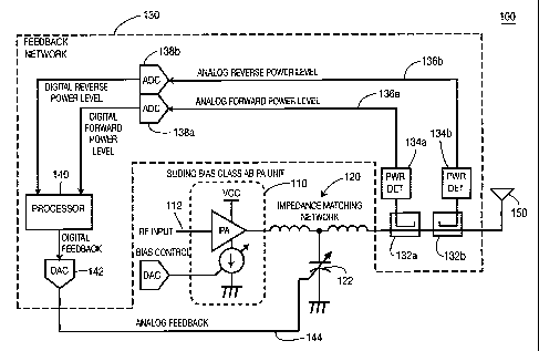
[0018] Figure 1 is a block diagram of an apparatus for dynamic load tuning
of a sliding bias class AB PA unit in accordance with one embodiment of the
present invention;
[0019] Figure 2 is a block diagram of an apparatus for dynamic load tuning
of a switch-mode PA unit in accordance with another embodiment of the present
invention;
[0020] Figure 3A is a block diagram of an apparatus for implementing one
of two PA modes using both the first and second stage PAs of a hybrid PA unit
in
accordance with another embodiment of the present invention;
[0021] Figure 3B is a block diagram of the apparatus of Figure 3A when it
implements the other one of the two PA modes using only the first stage PA and
bypassing the second stage PA of the hybrid PA unit;
[0022] Figure 4 is a flow diagram of a process including method steps for
matching impedance between a PA and an antenna in the apparatus of Figure 1,
based on power level feedback;
[0023] Figure 5 is a flow diagram of a process including method steps for
matching impedance between a PA and an antenna in the apparatus of Figure 2,
based on power level feedback; and
-3-
CA 02562111 2006-09-28
WO 2005/101678 PCT/US2005/009209
[0024] Figure 6 is a flow diagram of a process including method steps for
selectively bypassing a second amplification stage of a PA unit in the
apparatus
of Figure 3, based on power level feedback and TPC commands.
[0025] DETAILED DESCRIPTION OF THE PREFERRED EMBODIMENTS
[0026] Hereafter, the terminology "WTRU" includes but is not limited to a
UE, mobile station, fixed or mobile subscriber unit, pager, or any other type
of
device capable of operating in a wireless environment.
[0027] When referred to hereafter, the terminology base station includes
but is not limited to an access point (AP), a Node-B, site controller or any
other
type of interfacing device in a wireless environment. The invention is
particularly applicable to wireless local area networks (WLAN).
[0028] The features of the present invention may be incorporated into an
IC or be configured in a circuit comprising a multitude of interconnecting
components.
[0029] Figure 1 is a block diagram of an apparatus, (e.g., a transmitter),
100 for dynamic load tuning of a sliding bias class AB PA unit 110 in
accordance
with one embodiment of the present invention. The apparatus comprises the
sliding bias class AB PA unit 110, an impedance matching network 120 and a
feedback network 130.
[0030] As shown in Figure 1, the PA unit 110 receives an input signal via a
radio frequency (RF) input port 112 and outputs an amplified signal to an
antenna 150, (or an antenna array), through the impedance matching network
120. The PA unit 110 can be any type of amplifier, (e.g., a bipolar junction
transistor amplifier or a MOSFET amplifier). The antenna 150 receives the
amplified signal and wireless transmits it through an air interface. The
impedance matching network 120 is for matching an output impedance of the PA
unit 110 to an input impedance of the antenna 150. In order to transfer
maximum power to the antenna 150, the output impedance of the PA unit 110
should be matched to the input impedance of the antenna 150.
-4-
CA 02562111 2006-09-28
WO 2005/101678 PCT/US2005/009209
[0031] The impedance matching network 120 includes at least one
impedance adjustment device 122, (e.g., a variable capacitor), for adjusting
the
impedance of the network 120 to match the output impedance of the switch-mode
PA unit 110 to the input impedance of the antenna 150. The impedance
matching network 120 may include any known combination of devices, such as
capacitors, inductors, resistors, waveguide, or the like, to implement
impedance
matching between the PA unit 110 and the antenna 150.
[0032] As shown in Figure 1, the impedance adjustment device 122 is
adjusted by a feedback signal 142 generated by the feedback network 130. The
feedback network 130 generates the feedback signal after detecting a forward
power level transferred from the PA unit 110 and a reverse power level
reflected
back from the antenna 150. The exemplary feedback network 130 shown in
Figure 1 includes couplers 132a, 132b, power detectors 134a, 134b and a
processor 140. The couplers 132a, 132b couple a signal from the transmission
line from the impedance matching network 120 for feeding the antenna 150. Two
couplers 132a, 132b are provided for coupling a transmitting signal and a
reflecting signal.
[0033] As shown in Figure 1, the power level of the signals coupled by the
couplers 132a, 132b is detected by the power detector 134a, 134b. Two power
detectors 134a, 134b are provided for the forward power level 136a and the
reverse power level 136b, respectively. Alternatively, one power detector may
be
used in conjunction with a switch to selectively provide the forward and
reverse
power levels 136a, 136b, one at a time. The detected forward and reverse power
levels are converted by respective analog-to-digital converters (ADCs) 138a
and
138B, and are sent to the processor 140, which in turn provides a feedback
signal
144 to the impedance adjustment device 122 via a digital-to-analog converter
(DAC) 142. When an impedance mismatch occurs, the reverse power level 136b
increases compared to the forward power level 136a. Therefore, the processor
140 generates the feedback signal 144 in accordance with the increase of the
reverse power level 136b as compared to the forward power level 136a to
compensate for the changing load condition.
_5_
CA 02562111 2006-09-28
WO 2005/101678 PCT/US2005/009209
[0034] As shown in Figure 1, the feedback signal 144 enters the impedance
matching network 120 via the impedance adjustment device 122, the impedance
of which is adjusted in accordance with the feedback signal 144. The impedance
of the impedance adjustment device 122 may be adjusted continuously or
periodically. Alternatively, the impedance of the impedance adjustment device
122 may be adjusted when at least one of the forward power level 136a and the
reverse power level 136b exceeds a predetermined threshold.
[0035] Figure 2 is an exemplary block diagram of an apparatus, (e.g., a
transmitter), 200 for dynamic load tuning of a switch-mode PA unit 210 in
accordance with another embodiment of the present invention. The apparatus
200 comprises the switch-mode PA unit 210, an impedance matching network
220, and a feedback network 230.
[0036] As shown in Figure 2, the switch-mode PA unit 210 receives an
input signal via an RF input port 212 and outputs an amplified signal to an
antenna 250, (or an antenna array), through the impedance matching network
220. The antenna 250 receives the amplified signal and wirelessly transmits it
through an air interface. The impedance matching network 220 is for matching
an output impedance of the PA unit 210 to an input impedance of the antenna
250.
[0037] The impedance matching network 220 includes at least one
impedance adjustment device 222, (e.g., a variable capacitor), for adjusting
the
impedance of the network 220 to match the output impedance of the switch-mode
PA unit 210 to the input impedance of the antenna 250. The impedance
matching network 220 may include any known combination of devices, such as
capacitors, inductors, resistors, waveguide, or the like, to implement
impedance
matching between the PA unit 210 and the antenna 250.
[0033] As shown in Figure 2, the impedance adjustment device 222 is
adjusted by a feedback signal 244 generated by the feedback network 230. The
feedback network 230 generates the feedback signal 244 after detecting a
reverse
power level 255 reflected back from the antenna 250 and a direct current (DC)
level 260 consumed in the PA unit 210. The exemplary feedback network 230
-6-
CA 02562111 2006-09-28
WO 2005/101678 PCT/US2005/009209
shown in Figure 2 includes a coupler 232, a power detector 234 and a processor
236. The coupler 232 couples the impedance matching network 220 to the
antenna 250 and provides samples of signals reflected by the antenna to the
power detector 234.
[0039] The power level of the signals coupled by the coupler 232 is detected
by the power detector 234. The detected power level is sent to the processor
236.
The processor 236 also detects the DC level. The processor 236 generates a
feedback signal 244 from the detected reverse power level and the DC level.
When an impedance mismatch occurs, the reverse power level 255 increases and
the DC level 260 consumed by the PA unit 210 also increases with a departure
from an ideal output load. Therefore, the processor 236 generates the feedback
signal 144 in accordance with the increase of the reverse power level 255 and
the
DC level 260 to compensate for the changing load condition.
[0040] As shown in Figure 2, the feedback signal 244 is input to the
impedance matching network 220 via the impedance adjustment device 222, the
impedance of which is adjusted in accordance with the feedback signal 244. The
impedance of the impedance adjustment device 222 may be adjusted continuously
or periodically. Alternatively, the impedance of the impedance adjustment
device
222 may be adjusted when at least one of the reverse power level 255 and the
DC
level 260 exceeds a predetermined threshold.
[0041] Figures 3A and 3B are block diagrams of an apparatus, (e.g., a
transmitter), 300 for determining the optimum PA mode of a hybrid multi-stage
PA unit 310 in accordance with the present invention. The apparatus 300
comprises the hybrid PA unit 310 and a mode switching network 320. The
hybrid PA unit 310 comprises a first stage PA 312a connected in series to a
second stage PA 312b, a bypass network 314, a power detector 338, a threshold
comparator 340 and logic unit 342. The mode switching network comprises a
processor 325, a modem 330, a correction unit 332, a DAC 334 and a radio
transmitter 336 which provides an input signal 350 to the hybrid PA unit 310.
The output power from the hybrid PA unit 310 is fed to an antenna 380 via a
coupler 322 and a power detector 324 that respectively detect and measure the
_7_
CA 02562111 2006-09-28
WO 2005/101678 PCT/US2005/009209
output power level, and preferably convert it to a digital signal using an ADC
328
which provides a digital measurement of the output of the hybrid PA unit 310
to
the processor 325 which, in turn, generates a PA mode selection signal 355.
The
bypass network 314 is turned "on" and "off"' in accordance with the PA mode
selection signal 355.
[0042] The bypass network 314 includes at least two switches S1 and S2.
When the bypass network 314 is off, as illustrated by Figure 3A, the switch S1
connects the output of the first stage PA 312a to the input of the second
stage PA
312B, and the switch S2 connects the output of the second stage PA 312B to the
input of the coupler 322. When the bypass network 314 is turned on, as
illustrated by Figure 3B, the switches S1 and S2 bypass the second stage PA
312b and directly connect the output of the first stage PA 312a to the coupler
322.
[0043) The bypass network 314 is controlled by a bypass network control
signal 370 output by the logic unit 342. The first stage PA 312a supports a
different portion of the transmit power range of the hybrid PA unit 310 than
the
second stage PA 312b. The first stage PA 312a belongs to a different class
than
the second stage PA 312b. For example, the first stage PA 312a may be a
linear,
class AB PA, and the second stage PA 312b may be a switch-mode, class D, E or
F, PA. The first stage PA 312a is used to support a lower portion of the
transmitter operating, (output power), range, and the second stage PA 312b is
used to support a higher portion of the transmitter operating range. Thus, the
overall efficiency
[0044] The mode switching network 320 selectively switches, (i.e., based on
a switching hysterisis), the bypass network 314 on and off in accordance with
an
output power requirement. When a transmit power requirement is at a low level,
the mode switching network 320 turns on the bypass network 314, as shown in
Figure 3B, whereby the input signal is amplified only by the first stage PA
312a.
When a transmit power requirement is higher than a predetermined threshold,
the mode switching network 320 turns off the bypass network 314, whereby the
input signal 350 is amplified by both the first stage PA 312a and the second
stage
PA 312b, and thus the hybrid PA unit 310 operates in a different mode.
_g_
CA 02562111 2006-09-28
WO 2005/101678 PCT/US2005/009209
[0045] The mode switching network 320 may turn the bypass network 314
on and off based on the output power level of the hybrid PA unit 310. When the
output power from the hybrid PA unit 310 is lower than a predetermined
threshold, the mode switching network 320 turns on the bypass network 314,
whereby the input signal is amplified only by the first stage PA 312a. When
the
output power from the hybrid PA unit 310 is higher than a predetermined
threshold, the mode switching network 320 turns off the bypass network 314,
whereby the input signal is amplified by both the first stage PA 312a and the
second stage PA 312b.
[0046] The first stage PA 312a receives an input signal from a radio
transmitter 336 and outputs an amplified signal. The input of the second stage
PA 312b is connected to the output of the first stage PA 312a. The second
stage
PA 312b further amplifies the amplified signal output by the first stage PA
312a
when the bypass network 314 is off, as shown in Figure 3A.
[0047] Alternatively, the mode switching network 320 may turn the bypass
network 314 on and offbased on a transmit power control (TPC) command signal
365 provided by the modem 330. In a closed loop power control system, a
receiving station receives signals from a transmitting station and sends a TPC
command back to the transmitting station for transmit power control of the
transmitting station. The present invention utilizes the TPC command in
selecting an optimum mode of amplification. If a transmit power in accordance
with the TPC command signal 365 does not exceed a predetermined threshold,
0
the mode switching network 320 turns on the bypass network 314, whereby the
input signal is amplified only by the first stage PA 312a. When the transmit
power requirement in accordance with the TPC command is higher than a
predetermined threshold, the mode switching network 320 turns off the bypass
network 314, whereby the input signal 350 is amplified by both PAs 312a, PA
312b. The threshold for turning on and off may be set differently for
hysteresis.
[0048] When a TPC command is detected by the modem 330 in the mode
switching network 320, the TPC command is input to the processor 325 via the
TPC command signal 365. The processor 325 generates the PA mode selection
-9-
CA 02562111 2006-09-28
WO 2005/101678 PCT/US2005/009209
signal 355 based on the TPC command signal 355. The bypass network 314 is
turned on and off in accordance with the PA mode selection signal 355.
[0049] The hybrid PA unit 310 uses the power detector 338 and the
threshold comparator 340 for automatic mode switching. The power detector 338
detects a transmit power level output from the first stage PA 312a and the
detected power level is compared with a predetermined threshold by the
threshold comparator 340. If the transmit power output from the first stage PA
312a exceeds the predetermined threshold, the threshold comparator 340
generates a PA mode selection signal 360 to turn the bypass network 314 off:
If
the transmit power output from the first stage PA 312a falls below the
predetermined threshold, the threshold comparator 340 generates a PA mode
selection signal 355 to turn the bypass network 314 on, and the second stage
PA
312b is bypassed. The threshold for turning on and off the bypass network 314
may be set differently for hysteresis.
[0050] The hybrid PA unit 310 uses the logic unit 342 for combining the PA
mode selection signal 355 generated by the processor 325 and the PA mode
selection signal 360 generated by the threshold comparator 340.
[0051] Any instantaneous gain and insertion phase variations caused by
the mode switching of the hybrid PA unit 310 may be corrected in the digital
baseband by the correction unit 332. The correction unit 332 corrects the in-
phase (I) and quadrature (~) components of a signal 331 generated by the modem
330. Based on at least one signal received from the processor 325, the
correction
unit 332 outputs a signal to the radio transmitter 336 via the DAC 334
instructing the radio transmitter 336 to increase or decrease the output power
level of the input signal 350. For example, when the bypass network 314 is on,
the correction unit instructs the radio transmitter 336 to increase the power
level
of the input signal 350.
[0052] The present invention has an advantage of high integration and
possibility of using a single chip transceiver solution by reducing the PA
complexity, size, and heat dissipation. The present invention results in
higher
yield by increasing immunity to component variations while maintaining
-10-
CA 02562111 2006-09-28
WO 2005/101678 PCT/US2005/009209
performance, and improves the overall transmitter efficiency and extends
battery
life.
[0053] Figure 4 is a flow diagram of a process 400 including method steps
for matching impedance between a PA unit 110 and an antenna 150 in the
apparatus 100 shown in Figure 1, based on power level feedback. The PA unit
110 receives an input signal 112 (step 402), amplifies the input signal 112
(step
404), and transfers the amplified input signal to the antenna 150 (step 406)
via
the impedance matching network 120. The forward power level 136a from the
PA unit 110 and the reverse power level 136b reflected back from the antenna
140 are measured (step 408). A feedback signal 144 is generated based on the
forward power level 136a and the reverse power level 136b measurements (step
410). The impedance of the matching network 120 is adjusted in accordance with
the feedback signal 144 such that the output impedance of the PA unit 110 is
matched to the input impedance of the antenna 150 (step 412).
[0054] The forward power level 136a and the reverse power level 136b may
be converted from analog to digital signals via ADCs 138a and 138b,
respectively,
and input to the processor 140. The processor then outputs a digital feedback
signal, which may be converted to an analog feedback signal 144 via the DAC
142
for adjusting the impedance adjustment device 122 of the impedance matching
network 120. The impedance of the impedance adjustment device 122 in the
impedance matching network 120 may be adjusted either continuously or
periodically. Alternatively, the impedance adjustment device 122 may be
adjusted when at least one of the forward power level 136a and the reverse
power
level 136b exceeds a predetermined threshold.
[0055] Figure 5 is a flow diagram of a process 500 including method steps
for matching impedance between a PA unit 210 and an antenna 250 in the
apparatus 200 shown in Figure 2, based on power level feedback. The PA unit
210 receives an input signal 212 (step 502), and amplifies the input signal
(step
504). The amplified signal is transferred to the antenna 250 (step 506). A
reverse power level 255 reflected back from the antenna 250 and a DC level 260
consumed in the PA unit 210 are measured (step 508). Based on the reverse
-11-
CA 02562111 2006-09-28
WO 2005/101678 PCT/US2005/009209
power level 255 and the DC level 260, a feedback signal 244 is generated (step
510). The impedance of the impedance matching network 220 is adjusted in
accordance with the feedback signal 244 such that the output impedance of the
PA unit 210 is matched to the input impedance of the antenna 250 (step 512).
[0056] The reverse power level 255 and the DC level 260 may be converted
from analog to digital signals. The feedback signal 244 in digital form may be
converted back to an analog signal for adjusting the impedance adjustment
device 222 of the impedance matching network 220. The impedance adjustment
device 222 in the impedance matching network 220 may be adjusted either
continuously or periodically. Alternatively, the impedance adjustment device
may be adjusted when at least one of the reverse power level 255 and the DC
level 260 exceeds a predetermined threshold.
[0057] Figure 6 is a flow diagram of a process 600 including method steps
for determining the optimum PA mode of the hybrid PA unit 310 in the
apparatus 300 shown in Figure 3. In step 602, a hybrid PA unit 310 including a
first stage PA 312a and a second stage PA 312b is provided. The first stage PA
312a has an output connected to an input of the second stage PA 312b. The PAs
312a, 312b are of different classes and are connected in series. Each of the
PAs
312a, 312b supports a different portion of the transmit power range of the
hybrid
PA unit 310.
[0058] The gain provided by the hybrid PA unit 310 is controlled by
received TPC commands, whereby the second stage PA 312b is selectively
bypassed and/or disabled based on the requirements of the TPC commands.
[0059] Still referring to Figure 6, a TPC command is received at the modem
330 and forwarded to the processor 325 (step 604). In step 606, the power
level of
the output of the first stage PA 312a is measured by the power detector 338
for
use by the threshold comparator 340 (step 608). In step 608, the output power
level of, (i.e., the transmit power), of the entire hybrid PA unit 310 is
measured
by the power detector 324 for use by the processor 325. In step 610, the logic
unit
342 determines whether or not to bypass the second stage PA 312b based on at
least one of the received TPC command received in step 604, (i.e., the PA mode
-12-
CA 02562111 2006-09-28
WO 2005/101678 PCT/US2005/009209
selection signal 355), the output power level measurement of the first stage
PA
312a, (i.e., the PA mode selection signal 360), and the output power level
measurement of the entire hybrid PA 310 as detected by the power detector 324.
[0060] Although the features and elements of the present invention are
described in the preferred embodiments in particular combinations, each
feature
or element can be used alone without the other features and elements of the
preferred embodiments or in various combinations with or without other
features
and elements of the present invention.
[0061] While the present invention has been described in terms of the
preferred embodiment, other variations which are within the scope of the
invention as outlined in the claims below will be apparent to those skilled in
the
art.
-13-