Note: Descriptions are shown in the official language in which they were submitted.
CA 02562155 2012-05-29
-1-
PHOTOIONIZATION DETECTOR
Cross-Reference to Related Application
[0001] This application claims the benefit of U.S. Provisional Patent
Application
No. 60/557,921 filed March 31, 2004.
Background of the Invention
[0002] The present invention relates generally to photoionization detectors,
to
ionization chambers for use in photoionization detectors, and to methods of
use of
photoionization detectors.
[0003] Several photoionization detectors are described, for example, in US
Patent
Nos. 4,013,913; 4,398,152; 5,561,344; 6,225,633 and 6,646,444; and in German
Patent DE
19535216 Cl. In a typical photoionization detector (PID), a miniature gas-
discharge lamp is
used to produce high-energy vacuum ultraviolet (VUV) photons. In one approach,
a large
high-frequency voltage is applied between electrodes which are adjacent to the
lamp bulb in
order to induce an ionization, excitation and photoemission process in the gas
which is sealed
within the lamp bulb. Some of the resulting VUV photons pass through a VUV-
transmissive
window in the lamp to illuminate an adjacent volume within an electrically-
biased ionization
chamber, into which a sample of gas is introduced. Depending on the ionization
potentials of
the various species in the sampled gas and the maximum photon energy of the
VUV
radiation, photoionization of some of the gas molecules introduced into the
ionization
chamber can thus occur and be detected. An electrodeless (that is, having no
internal
electrodes), miniature PID gas discharge lamp is described, for example, in US
Patent
5,773,833.
CA 02562155 2006-09-20
WO 2005/098413 PCT/US2005/010910
-2-
[0004] Typically the ionization chamber of a PID is constructed with a housing
formed integrally within the PID sensor, and at least one pair of closely-
spaced electrodes is
positioned within the ionization chamber. The gas to be analyzed is introduced
into the
chamber through at least one gas inlet and leaves the chamber through at least
one gas outlet.
The window of the lamp is positioned so as to illuminate the sampled gas
molecules with
VUV photons as they move toward or within the volume between the ionization
chamber
electrodes. A voltage applied between these electrodes generates a high
electric field across
their gap, which forces the ions and electrons resulting from the
photoionization process to
move toward the lower or higher potential electrode, respectively. Usually an
electrometer
circuit is used to measure the ion current flowing to the cathode electrode.
The presence of
photo-ionizable molecules in the sampled gas is thereby detected. The
sensitivity of a
particular PID design to a variety of ionizable compounds can be determined
relative to its
calibrated sensitivity to a standard compound. The use of a hand-held PID
device to detect
trace levels of volatile organic compounds (VOCs) is one particularly
important application
of this technique.
[0005] It is well known that the presence of water vapor in the gas flow (as
quantified
by the relative humidity) can alter the sensitivity and the background signal
level of a PID.
Various techniques have been developed to reduce or correct for this effect.
For instance,
U.S. Patent No. 4,778,998, assigned to Mine Safety Appliances Company,
describes a PID in
which a humidity sensor, a temperature sensor and a microcomputer
(microprocessor) are
used to apply a predetermined correction factor to compensate for the cross-
sensitivity of the
PID to the relative humidity.
[0006] As a PID lamp is operated with its window exposed to trace hydrocarbon
and
organo-silicone compounds in a sample of ambient air, the window surface tends
to become
increasingly contaminated by a surface film which is formed from the
photoionization
products of these air-borne compounds. This causes the effective lamp output
intensity to
decrease slowly with operating time. The typical maintenance procedure for PID
instruments
CA 02562155 2006-09-20
WO 2005/098413 PCT/US2005/010910
-3-
thus requires removal of the lamp and cleaning of the window manually when the
sensitivity
has dropped below a certain level.
[0007] Current types of PID instruments have several substantial
disadvantages. For
example, U.S. Patent Nos. 5,773,833 and 6,225,633 disclose multilayer=
ionization chambers
for a PID which are fabricated from multiple layers of machined PTFE and
stainless steel,
making the ionization chambers relatively difficult and expensive to
manufacture. In those
designs, the multilayer ionization chambers are held together by metallic
pins. The metallic
pins also function as electrical contacts for the ionization chamber and
removably attach the
sensor ionization chamber to the remainder of the instrument. Ionization
chambers similar to
those described in U.S. Patent Nos. 5,773,833 and 6,225,633 are found for
example in the
TOXIRAE PLUS and MULTIRAE PLUS instruments available from RAE Systems, Inc. of
Sunnyvale, California.
[0008] Furthermore, with extended operating time the electrodes within the
ionization
chamber become contaminated by the process described above, resulting in
leakage currents
and inaccurate measurements. It is quite difficult and relatively expensive to
repair or restore
an ionization chamber by opening it and removing this contamination. For
example, as
described in the Operation Manual for the TOXIRAE PLUS sensor, its sensor
ionization
chamber can be gently removed from the instrument for cleaning, and the
ionization chamber
is to be cleaned in a methanol bath (an ultrasound bath is highly
recommended). After
cleaning, the sensor ionization chamber can be reattached to the remainder of
the instrument.
Precise alignment of the sensor ionization chamber with dedicated pin contact
seatings in the
remainder of the instrument is required for reattachment of the TOXIRAE PLUS
and
MULTIRAE PLUS sensor ionization chambers.
[0009] As an alternative to manual cleaning, an enhanced concentration of
ozone is
purported to loosen or remove organic deposits from these surfaces to some
degree.
Schemes for self-cleaning the ionization chamber and the VUV lamp window,
which rely on
operating the VUV lamp during exposure to an oxygen-containing atmosphere in
order to
CA 02562155 2006-09-20
WO 2005/098413 PCT/US2005/010910
-4-
generate ozone, have been described. See for example U.S. Patent No.
6,313,638. However,
these self-cleaning schemes also present disadvantages, which are discussed
below.
[0010] Depending on the minimum wavelength that must be transmitted, only a
small
number of crystalline materials, such as CaF2, BaF2, MgF2 or LiF, are usable
as VUV
windows for PID lamps. The transmission of these VUV window materials reduces
sharply
below about 140 nm. The shortest wavelength transmission is provided by LiF
optical
material, but the transmission of LiF is degraded over time by color-center
formation
("solarization") in the crystal due to exposure to the VUV radiation. Indeed,
product
specifications for a miniature LiF-window PID gas-discharge lamp which is
available from
RAE Systems, Inc., of Sunnyvale, California, indicate that the lamp is limited
to an operating
life of less than several hundred hours.
[0011] An alternative method is described in US Patent No. 6,255,633 for
producing a
self-cleaning action on the VUV lamp window and on the internal surfaces of
the ionization
chamber in a PID device. This requires stopping the gas flow in the ionization
chamber and
operating the VUV lamp to produce a higher concentration of ozone in the
static sample.
However, for a lamp with a LiF window this method exacerbates degradation of
the LiF
material due to color-center formation by the VUV radiation, and the repeated
self-cleaning
cycles will use up a significant fraction of its limited available operating
life. This reduction
of the useful operating life applies to a lesser extent to any type of VUV
lamp which is self-
cleaned by methods similar to that of US Patent No. 6,255,633.
[0012] For the above reasons it is therefore desirable to develop improved
photoionization detectors, ionization chambers for use in photoionization
detectors, and
methods of use and assembly of photoionization detectors.
Summary Of The Invention
[0013] In one aspect, the present invention provides a photoionization
detector
including a housing, electrical contacts within the housing and a
photoionization chamber
CA 02562155 2006-09-20
WO 2005/098413 PCT/US2005/010910
-5-
within the housing. The photoionization chamber includes a cathodic electrode
and an
anodic electrode. The photoionization chamber and the associated cathodic
electrode and
anodic electrode are removable from within the housing as a unit. The
photoionization
chamber makes electrical connection with the contacts when in the housing
regardless of the
orientation of the photoionization chamber about its axis. The photoionization
detector also
preferably includes a lamp to transmit VUV energy to within the
photoionization chamber.
[0014] In one embodiment, a side of the cathodic electrode which attracts
positively
charged reaction products is coated with a layer of a nonconductive material.
The layer of
nonconductive material allows the detection of at least a portion of the
positively charged
reaction products impinging upon the layer. The layer of non-conductive
material on the
cathodic electrode can also be VUV absorptive. A side of the anodic electrode
which repels
positively charged reaction products can also or alternatively be coated with
a layer of
nonconductive material. Once again, the layer of material on the anodic
electrode can also
be VUV absorptive. Preferably, such layers of material on the cathodic
electrode and/or
anodic electrode are of generally uniform thickness over the coated area of
the electrode.
[0015] In a further embodiment, the photoionization chamber housing includes a
first
housing member in electrical connection with the cathodic electrode. At least
a portion of
the surface of the first housing member forms a first electrical contact. The
housing further
includes a second housing member in electrical connection with the anodic
electrode. At
least a portion of the surface of the second housing member forms a second
electrical contact.
The first housing member can be formed entirely from a conductive metal.
Likewise, the
second housing member can be formed entirely from a conductive metal. The
first housing
member and the second housing member can, for example, be mechanically
connected to an
insulating connector. Such a connector can be annular in shape. In one
embodiment, the
first housing member and the second housing member are mechanically connected
to an
annular, insulating connector via crimping.
CA 02562155 2006-09-20
WO 2005/098413 PCT/US2005/010910
-6-
[0016] In another aspect, the present invention provides a photoionization
chamber for
use within a housing of a detector including a cathodic electrode and an
anodic electrode
spaced from the cathodic electrode. The photoionization chamber also includes
a first
housing member, wherein at least a portion of the surface of the first housing
member forms
a first electrical contact in electrical connection with the cathodic
electrode. The
photoionization chamber further includes a second housing member, wherein at
least a
portion of the surface of the second housing member forms a second electrical
contact in
electrical connection with the anodic electrode. The second electrical contact
is electrically
insulated from the first electrical contact. The photoionization chamber is
removable from
the housing of the detector.
[0017] The first housing member and the second housing member can be
mechanically connected to a single connector. The first housing member can be
formed from
a conductive metal. Similarly, the second housing member can be formed from a
conductive
metal. As discussed above, the first housing member and the second housing
member can be
mechanically connected to an annular, insulating connector (via, for example,
crimping).
[0018] In a further aspect, the present invention provides a photoionization
detector
including a housing and a photoionization chamber within the housing. The
photoionization
detector also includes a first housing member and a second housing member. The
first
housing member and the second housing member are mechanically connected to a
single,
electrically insulating connector. The photoionization chamber further
includes a cathodic
electrode in electrical contact with the first housing member and an anodic
electrode in
electrical contact with the second housing member. The photoionization chamber
and the
included cathodic electrode and anodic electrode are removable from within the
detector
housing as a unit. The photoionization detector also preferably includes a
lamp to transmit
VUV energy into the photoionization chamber.
[0019] In another aspect, the present invention provides a photoionization
chamber
including a cathodic electrode and an anodic electrode. The cathodic electrode
includes a
CA 02562155 2006-09-20
WO 2005/098413 PCT/US2005/010910
-7-
layer of a nonconductive material coated upon a side of the cathodic electrode
which attracts
positively charged reaction products. The layer allows the detection of at
least a portion of
positively charged reaction products impinging upon the layer. The anodic
electrode
includes a layer of a nonconductive material coated on a side of the anodic
electrode which
repels positively charged photoionization reaction products into a volume
between the
cathodic electrode and the anodic electrode.
[0020] The present invention utilizes a VUV lamp including an enclosure
containing a
discharge gas or gas mixture. One or more portions of the enclosure include a
VUV
transmissive section of crystalline material to transmit VUV radiation. A
portion of the
enclosure can be fabricated from another material to which the crystalline VUV
transmissive
section(s) can be hermetically sealed. For example, the material can be glass,
ceramic or
quartz.
[0021] In still a further aspect, the present invention provides a
photoionization
detector including a housing, a photoionization chamber within the housing,
and a VUV
lamp to transmit VUV energy to within the photoionization chamber. The
photoionization
detector further includes at least one restrictive orifice in the gas flow
path into the ionization
chamber, such that a pressure on the photoionization chamber side of the
orifice is less than
the pressure on the other (inlet or ambient) side of the orifice. The
restrictive orifice(s)
reduce the relative humidity of sample gas within the photoionization chamber
as compared
to the relative humidity in the ambient environment, thereby making the
photoionization
chamber less sensitive to ambient relative humidity. In one embodiment, a
single restrictive
orifice is placed in the gas flow path. In another embodiment, a plurality of
restrictive
orifices are placed in the gas flow path. The plurality of restrictive flow
paths can, for
example, be formed in a filter (for example a porous frit) having a
correspondingly small
pore diameter.
CA 02562155 2006-09-20
- 7a-
In another aspect, the invention provides a photoionization detector
comprising: a housing; a photoionization chamber within the housing; a VUV
lamp
to transmit VUV photons to within the photoionization chamber; and at least
one
source of photons outside the VUV lamp which can be electrically activated to
illuminate an inner surface of the VUV lamp in order to enhance the
startability and
operational performance of said VUV lamp.
CA 02562155 2006-09-20
WO 2005/098413 PCT/US2005/010910
-8-
Brief Description Of The Drawings
[0022] Figure 1 illustrates a cutaway, perspective, exploded or disassembled
view of
an embodiment of a PID of the present invention.
[0023] Figure 2A illustrates a cutaway, side view of the PID of Figure 1 in an
assembled state, other than the top enclosure or cap.
[0024] Figure 2B illustrates a cutaway, perspective view of the PID of Figure
1 in an
assembled state, other than the top enclosure or cap.
[0025] Figure 2C illustrates a cutaway, perspective, exploded or disassembled
view
the PID of Figure 1 including an alternative electrode configuration.
[0026] Fig. 3A illustrates a perspective, partially exploded view of the PID
of Figure 1
in attachment to another instrument housing.
[0027] Fig. 3B illustrates a perspective, partially exploded view of selected
components of the PID of Figure 1 as they may be incorporated within the
housing of a
multi-sensor instrument assembly.
[0028] Figure 4A illustrates a top plan view of an embodiment of an ionization
chamber of the present invention.
[0029] Figure 4B illustrates a side, cross-sectional view of the ionization
chamber of
Figure 4A.
[0030] Figure 4C illustrates a perspective view of the ionization chamber of
Figure 4A.
[0031] Figure 4D illustrates a perspective, exploded view of the ionization
chamber of
Figure 4A.
CA 02562155 2006-09-20
WO 2005/098413 PCT/US2005/010910
-9-
[0032] Figure 5A illustrates a top plan view of another embodiment of an
ionization
chamber of the present invention.
[0033] Figure 5B illustrates a side, cross-sectional view of the ionization
chamber of
Figure 5A.
[0034] Figure 5C illustrates a perspective view of the ionization chamber of
Figure 5A.
[0035] Figure 5D illustrates a perspective, exploded view of the ionization
chamber of
Figure 5A.
[0036] Figure 6A illustrates a top plan view of another embodiment of an
ionization
chamber of the present invention.
[0037] Figure 6B illustrates a side, cross-sectional view of the ionization
chamber of
Figure 6A.
[0038] Figure 6C illustrates a perspective view of the ionization chamber of
Figure 6A.
[0039] Figure 6D illustrates a perspective, exploded view of the ionization
chamber of
Figure 6A.
[0040] Figure 7A illustrates a top plan view of another embodiment of an
ionization
chamber of the present invention.
[0041] Figure 7B illustrates a side, cross-sectional view of the ionization
chamber of
Figure 7A.
[0042] Figure 7C illustrates a perspective view of the ionization chamber of
Figure 7A.
CA 02562155 2006-09-20
WO 2005/098413 PCT/US2005/010910
-10-
[0043] Figure 7D illustrates a perspective, exploded view of the ionization
chamber of
Figure 7A.
[0044] Figure 8 illustrates a perspective, exploded view of another embodiment
of an
ionization chamber of the present invention.
[0045] Figure 9 illustrates a perspective, exploded view of another embodiment
of an
ionization chamber of the present invention, which allows for an alternative
gas flow path.
DETAILED DESCRIPTION OF THE INVENTION
[0046] Figures 1 through 2B illustrate an embodiment of a PID 10 of the
present
invention, which can, in one embodiment include a detector housing 20 and a
cooperating top
enclosure or cap 30. Cap 30 can, for example, be maintained in connection with
housing 20
via connectors such a screws 22. In the embodiment of Figures 1 through 2B,
guides 24 (for
example, annular members) guide screws 22 through a generally cylindrical
screw well 26 to
connect to cap 30.
[0047] As shown in Figure 3A, housing 20 can also be connected to another
housing 520 of an instrument 500, which can, for example, include one or more
other gas
sensors. Such other sensors can, for example, be electrochemical gas sensors.
An
embodiment of an ionization chamber 200a for use in a multi-sensor instrument
is shown, for
example, in more detail in Figs. 5A-5D. As shown in Figure 3B, the components
of PID 10
can alternatively be incorporated within the housing 620 of a multi-sensor
instrument
assembly 600. In either case, some or all of the other gas sensors 630 may be
supplied with
the same sample of analyte gas as the PID sensor which is described in further
detail below,
for example, by diffusion or via flow forced by a pump (not shown in Figure
3B) through a
connection fitting 640. In Figure 3B, vacuum ultraviolet radiation (VUV) lamp
40 and the
photoionization chamber assembly 200a (see Figure 5) of a type viable for use
in PID 10 are
separately removable from the instrument housing for service or replacement by
removing an
internal cover piece 650 and an external cover piece 660. A filter for
airborne particulates
CA 02562155 2006-09-20
WO 2005/098413 PCT/US2005/010910
-11-
and droplets (not shown) can be positioned in the path of the sample gas
before it enters the
ionization chamber. Furthermore, the present inventors have discovered that
the sensitivity
of the PID to humidity in the air can be reduced by causing a pressure
differential/drop across
the inlet to the ionization chamber. Such a pressure drop results in a
decrease in relative
humidity. Preferably, the pressure drop is sufficient to cause at least a 5%
drop in relative
humidity. More preferably, the pressure drop is sufficient to cause at least a
10% drop in
relative humidity. Such a pressure drop and the associated drop in relative
humidity can be
accomplished by positioning one or more restrictive orifices in the gas flow
path into the
ionization chamber, so that a pressure differential is developed across the
orifice(s). Such an
orifice 652 can be provided, for example, in the internal cover piece 650 as
illustrated in
Figure 3B. Alternatively, for example, a filter with a relatively small pore
diameter/size can
be used (thereby providing a plurality of orifices of restricted diameter) to
create a pressure
drop across the inlet to the photoionization chamber.
[00481 In the embodiment of Figures 1 through 2B, a VUV lamp 40 is slidably
and
removably disposed within an insulating lamp sleeve 50 and rests at its bottom
end upon a
lamp pad, seating or spring 60. For example, spring 60 can be a piece of semi-
soft tubing
which captures and axially centers lamp 40 at its bottom end 40a, and may
simultaneously
make a gas-flow seal between the lamp envelope and the insulating sleeve 50.
In the
embodiment shown in Figure 2C, cap 60b attaches by a screw thread (not shown)
to housing
section 20a, and is removable by the user to provide easy access to removable
lamp 40. An
external or internal shoulder 60c can be provided on cap 60b, in order to fix
the required
depth of insertion of cap 60b into housing 20 and thereby provide the required
compressive
force on lamp seating or spring 60a of Figure 2C. In the embodiments shown in
Figures 1
through 2C, lamp sleeve 50 can be sealed against lamp electrode 70 or base 150
using a
sealing compound. In another embodiment, the gasket pad 140 can be configured
to project
radially into passage 100 to seal against lamp sleeve 50 or the envelope of
lamp 40.
CA 02562155 2006-09-20
WO 2005/098413 PCT/US2005/010910
-12-
[0049] The VUV lamp 40 can be of a type which operates with electrodes inside
the
lamp envelope, or of a type which operates without internal electrodes. In the
preferred
embodiment shown, a low-pressure gas discharge is induced within VUV lamp 40
by
applying appropriate voltage levels to external electrodes 70 and 80, as known
in the art. In
the embodiment of Figures 1 through 2B, electrode 70 is a disk-shaped
electrode and
electrode 80 is a composite electrode including electrode sections 80a and
80b. When
assembled, electrode section 80b attaches into the opening of electrode
section 80a to form a
single, cup-shaped electrode 80, as shown, for example, in Figure 2B. AC power
can, for
example, be transmitted to VUV lamp 40 via rear electrode 80 or via forward
electrode 70.
Figure 2C illustrates an alternative embodiment in which electrode 80' is
formed as a sleeve.
PID 10 can, for example, include a power supply, such as a DC battery which is
in
connection with a DC to AC converter as known in the art.
[0050] Photons generated within VUV lamp 40 are transmitted through a VUV
window 90 (at the top of lamp 40 in the orientation shown in Figures 1 through
2C).
Window 90 can be fabricated from a VUV transmissive crystalline material such
as, but not
limited to, CaF2, BaF2, MgF2 or LiF. Several established methods are available
for affixing
a VUV crystal window to a glass tube body to form a low-pressure gas-discharge
lamp.
These methods include, for example, glass-to-glass seals and adhesive seals.
[0051] It is known that electrodeless gas discharge lamps can be more
difficult to start
at low temperatures or when the gas-filled volume is shielded from any
external illumination.
Under those conditions it can be more difficult to generate the initial free
electrons which
will lead to an electrical discharge in the fill gas of the lamp. Several
methods are known in
the art which will help to enhance the startability of the lamp when its
starting voltage is
applied. Those methods include heating the lamp; altering the gas fill of the
lamp with a
plurality of gasses; providing a radioactive source of ionizing particle
radiation; and/or
providing an electric-field enhancing metal object within or adjacent to the
discharge
volume.
CA 02562155 2006-09-20
WO 2005/098413 PCT/US2005/010910
-13-
[0052] It is also generally understood that illuminating an additional inner
conductive
surface region of the discharge volume with externally generated photons of
sufficient energy
to produce electro-thermal enhanced photo-electron emission from the
illuminated surface
regions will help to enhance startability of the lamp. The inventors of the
present invention
have discovered that another method of enhancing startability and operational
performance
can be provided, for example, by a near-UV or UV light energy source 41 (see
Figure 2C)
such as a light-emitting diode (LED). The photons from light energy source 41
are directed
through a transparent portion of the envelope of lamp 40, without the use of a
conductive
surface inside the lamp envelope upon which the photons would impinge. Light
energy
source 41 can be positioned within housing 20 adjacent to lamp 40, or it can
be positioned
remote from lamp 40 (and even exterior to housing 20) with the light
transmitted to the
transparent section of lamp 40 via a light transmitting pathway such as a
fiber optic line or a
light pipe (not shown in Figure 2C).
[0053] VUV lamp 40 inserts into a passage 100 formed in an ionization chamber
enclosure 110, so that its emitted VUV radiation enters a photoionization
chamber 200 via an
opening 222 formed in the exterior bottom of ionization chamber 200 (in the
orientation of
Figures 1 through 2C), which the lamp window 90 abuts or comes close to. Lamp
40 can be
provided with an internal piece of getter material (not shown) to better
maintain the purity of
the internal gas, as known to those skilled in the art.
[0054] Enclosure 110 includes a lower (in the orientation of Figures 1 through
2C)
seating 120 and an upper cover 130. A sealed connection can be maintained
therebetween
via, for example, a seal 140 (for example, a gasket). In the embodiment of
Figures 1 through
2C, seating 120 and gasket 140 are connected to a base 150, for example, a
printed circuit
board. Analyte gas from the surrounding environment enters ionization chamber
200 via an
inlet 132 formed in upper cover 130 of the enclosure 110. Preferably, a seal
160 (for
example, an O-ring) forms a sealed passage between inlet 132 and a gas inlet
212 formed in
ionization chamber 200. Preferably, another seal 170 (for example, an O-ring)
forms a
CA 02562155 2006-09-20
WO 2005/098413 PCT/US2005/010910
-14-
sealed passage between an analyte gas inlet 32 formed in cap 30 and inlet 132.
Analyte gas
can pass into ionization chamber 200 via sequential inlets 32, 132 and 212 via
diffusion or
via forced flow (using a pump; see, for example, Figure 1) as known in the
art. Another gas
seal is provided by gasket 140 pressing against the lamp sleeve 50.
Alternatively, the
opening of the lamp sleeve 50 can be sealed against electrode 70 or base 150
using a sealing
compound, and the gasket 140 can seal against the body of lamp 40. In the
embodiment of
Figures 1 through 2C, gas exits photoionization chamber 200 via one or more
outlets 214a
and 214b. Such gas exits PID 10 via exhaust tube 180, which is in fluid
connection with an
exhaust vent 190.
[0055]Unlike most ionization chambers used in currently available PIDs (in
which the
photoionization chamber is generally integral with the remainder of the PID),
ionization
chamber 200, including the electrodes therein, is readily removable from PID
10 and
replaceable as a unit or a module. Moreover, photoionization chamber 200 and
other
photoionization chambers of the present invention are relatively simple and
inexpensive to
manufacture, thereby making it relatively inexpensive to dispose of
contaminated
photoionization chambers of the present invention and replace those
photoionization
chambers with new photoionization chambers of the present invention. Further,
the
photoionization chambers of the present invention are, in many embodiments,
easily
removable and readily insertable within a PID or other instrument of the
present invention,
without the need for careful alignment of corresponding electrical contacts
and/or mechanical
connections. Several embodiments of the photoionization chambers of the
present invention
are discussed in further detail below in connection with Figures 4A through 9.
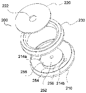
[0056] Referring to Figures 4A through 4D, in one embodiment, photoionization
chamber 200 includes a first housing member 210 and a second housing member
220. First
and second housing members 210 and 220, respectively, can be mechanically
connected via,
for example, a single mechanical connector such as a gasket ring 230 to create
a sealed
photoionization chamber 200 having a chamber volume 240.
CA 02562155 2006-09-20
WO 2005/098413 PCT/US2005/010910
-15-
[0057] Inlet 212, by which the analyte molecules and their carrier gas enter
into
photoionization chamber 200 as described above, is formed in first housing
member 210.
Once again, the design of inlet port 212 can be chosen as known in the art to
allow for
diffusive entry of the analyte molecules, or for a metered flow of carrier gas
driven by a gas
pump on the downstream or upstream side of photoionization chamber 200. One or
more
exit openings such as outlets 214a and 214b can be formed in, for example,
first housing
member 210 for a flow or diffusion path by which the analyte molecules and
their carrier gas
can exit from photoionization chamber 200. Alternatively, the pumped flow of
carrier gas
can be in the reverse direction, in which case the one or more ports 214a and
214b will be the
inlet port(s), and port 212 will be the outlet port. When operated in a
diffusion mode, a
single port (for example, port 212) can operate as both the inlet port and the
outlet port. A
microporous filter (not shown) may be used in the path of the carrier gas
flowing into the
photoionization chamber 200, as known in the art.
[0058] In the orientation of Figure 4B, chamber volume 240 is partly bounded
by an
upper surface of a cathodic "ion collector" electrode 250 to which positively
charged reaction
products are attracted. Cathodic electrode 250 can, for example, be formed on
or connected
to one side of an insulating disk 254. Cathodic collector electrode 250 can be
mechanically
connected and/or integrated with first housing member 210. Cathodic collector
electrode 250
and housing member 210 can also be electrically connected if first housing
member 210 is
chosen to be conductive. In the embodiment of Figures 4A through 4D, cathodic
collector
electrode 250 and insulating disk 254 typically include a typically central
passage 252
through which analyte molecules passing through inlet 212 enter chamber volume
240. A
lower surface of an anodic "ion repeller" electrode 260, formed on or
connected to an interior
surface of second housing member 220, is spaced from the upper surface of
cathodic
electrode 250 to further define chamber volume 240. In the embodiment of
Figures 4A
through 4D, anodic electrode 260 and second housing member 220 rest on a ledge
232
formed in gasket 230 to space anodic electrode 260 from cathodic electrode
250. In one
CA 02562155 2012-05-29
-16-
embodiment, each of cathodic electrode 250 and anodic electrode 260 were
fabricated from
stainless steel.
[0059] First housing member 210 can, for example, be at least partially
fabricated
from a thin non-magnetic stainless steel for the purposes of electrical
connection and
electromagnetic shielding. The assembly of first housing member 210 and second
housing
member 220 is similar to the assembly of the "button cell" electrochemical
sensors described
in U. S. Patent No. 5,667,653, assigned to the assignee of the present
invention.
For example, after assembly of the parts
thereof, a rim 216 of first housing member 210 can be pressed radially inward
or crimped
against a single mechanical connector such as gasket 230 to create a leak-
proof mechanical
seal therebetween. Connector or gasket 230 can be fabricated from an
insulating material to
provide electrical insulation between first housing member 210 and second
housing
member 220. The fabrication technique of the present invention is less
complicated, faster
and less expensive than prior fabrication techniques for photoionization
chambers.
[0060] An electrical connection from the cathodic electrode 250 to first
housing
member 210 can be provided. This connection can, for example, be accomplished
by plating
passage 252 or by providing one or more other conductive paths through the
thickness of
insulating disk 254. Alternatively, disk 254 can be entirely conductive, in
which case it
serves as the cathodic electrode, and a distinct electrode element 250 is not
needed on its
surface. Likewise, an electrical connection from anodic electrode 260 to the
external surface
of second housing member 220 can be provided. This connection can, for
example, be
accomplished by providing one or more conductive paths through the thickness
of an
insulating second housing member 220 to connect to one or more conductive
areas on the
opposing side of second housing member 220. Second housing member 220 can
alternatively be made entirely conductive, in which case it serves as the
anodic electrode, and
a distinct electrode element 260 is not needed on its surface.
CA 02562155 2006-09-20
WO 2005/098413 PCT/US2005/010910
-17-
[0061] In one embodiment, first housing member 210 and disk 254 are conductive
and
electrically connected, and first housing member 210 forms an electrical
connection with one
or more electrical connections 192 of seating 120 (see Fig. 1). In a further
embodiment,
second housing member 220 is conductive and serves as the anodic electrode. In
this
embodiment, second housing member 220 forms an electrical connection with one
or more
other electrical connections 194 of seating 120 in a manner similar to a
battery in a battery
holder. Cover 130 can be metal that is grounded to form an electrical shield.
Second
housing member 220 can be conductive over at least a part of its external
surface for the
purpose of electrical connection.
[0062] In several embodiments, the conductive portions of each of first
housing
member 210 and second housing member 220 (and other housing members of the
photoionization chambers of the present invention), which can be the entirety
thereof, extend
annularly (although not necessarily symmetrically) around axis A so that no
specific
rotational alignment of photoionization chamber 200 about axis A is required
to form
electrical contacts within, for example, PID 10 as described above. Moreover,
as the surface
of the housing members can act as electrical contacts in several embodiments
of the
photoionization chambers of the present invention, there is no requirement for
alignment in
any orientation or plane of extending electrical contacts such as pins.
[0063] As described above in connection with PID sensor 10, VUV radiation from
gas
discharge lamp 40 enters photoionization chamber 200 through opening or inlet
222 in
second housing member 220. In one embodiment, lamp 40 is an electrodeless
sealed glass
tube filled with a particular low-pressure discharge gas or gas mixture as
known in the art.
One portion or end of the glass lamp tube is sealed with a VUV-transmissive
crystalline
section or window 90 which can abut second housing member 220 over, for
example, a
generally circular area around inlet 222. Although second housing member 220
can be made
entirely conductive, it can be advantageous to form at least the portion
thereof contacted by
CA 02562155 2006-09-20
WO 2005/098413 PCT/US2005/010910
-18-
window 90 from a material with a very low quantum efficiency for production of
photoelectrons (see, for example, Figures 7A through 7D discussed below).
[0064] It can also be beneficial to coat at least the cathodic electrode 250
on its ion-
collecting side with a thin (for example several tens of microns) and
generally uniform
layer 256 of substantially VUV-absorptive material, such as
polytetrafluoroethylene (PTFE),
to suppress the production and/or emission of photoelectrons from cathodic
electrode 250 as
a result of the VUV radiation from lamp 40. Cathodic electrodes on some
currently available
PIDs (for example U.S. Patent No. 5,773,833) are thin and perforated for the
through-
diffusion of analyte ions, with the VUV-absorbing coating only on the side
thereof facing the
VUV lamp. However, the inventors of the present invention have discovered that
a thin
layer 256 on the ion-collecting side of cathodic electrode 250 of the present
invention
performed the VUV-blocking function, while still allowing the detection of
positively
charged reaction products by their impingement onto and/or through layer 256
on cathodic
electrode 250. Anodic electrode 260 can also be provided with a similarly thin
layer 266 of
an insulating material, which may also be substantially VUV-absorptive.
Insulating
layers 256 and/or 266 can be extended along the underlying surfaces to assist
in preventing
current leakage between electrodes 250 and 260. These electrode coating layers
can also be
slightly conductive. Allowing for a slightly conductive electrode layer will
affect the amount
of current leakage. The coatings can, for example, be made of PTFE which
contains carbon
particles, or any other similar construction.
[0065] The PIDs of the present invention can optionally be supplied with bare
metal
for the cathode and/or anode surfaces which face the electrode gap. Even in
the case of
uncoated electrode surfaces, the quantum efficiency for VUV production of
photoelectrons is
mitigated somewhat by the thin metal oxide film which naturally forms on metal
surfaces
which have been exposed to air. The formation of this beneficial metal oxide
film can
preferably be expedited by heating the metal electrode parts in air at a high
temperature for
up to several hours.
CA 02562155 2006-09-20
WO 2005/098413 PCT/US2005/010910
-19-
[0066] PID 10 further includes circuitry as known in the art to: (a) provide
independent steady or varying voltages to cathodic electrode 250 and to anodic
electrode 260
of ionization photoionization chamber 200; (b) measure an output signal at the
level of, for
example, picoamperes resulting from impact of positive ions on cathodic
electrode 250
during operation of PID 10; and (c) provide independent steady or varying
voltages to the
electrodes of gas discharge lamp 40. Lamp 40 is typically driven at a
sinusoidal frequency in
the kilohertz to megahertz range, as known in the art. In one method, the
amplitude of the
sinusoidal lamp voltage can be modulated to reduce the average power to the
lamp, as known
in the art (see for example U.S. Patent No. 5,773,833).
[0067] The ionization chambers of the present invention can also be used with
alternative means of producing the necessary ionization of analyte molecules
within chamber
volume 240. Examples of such other means include multi-step ionization by one
or more
laser beams, injection of metastable excited gas species and/or VUV photons
from a
discharge or spark chamber into ionization chamber 200 (see for example U.S.
Patent Nos.
5,541,519 and 6,333,632), low activity radioactive sources of ionizing
particles (see for
example U.S. Patent No. 4,704,336), or electrical field ionization of the
analyte molecules by
applying brief high-voltage pulses via electrodes 250 and 260. Other means of
producing
ionization can be recognized by those skilled in the art.
[0068] As set forth above, readily removable (and easily reinsertable)
photoionization
chamber 200 of the present invention enables quick and inexpensive
remedying/repair of
PID 10 in which photoionization chamber 200 has become contaminated, by simple
replacement of photoionization chamber 200. Moreover, the removable and
replaceable
nature of the photoionization chambers of the present invention allow PID 10
to be adjusted
for different environmental or ambient conditions as well as certain manners
of use of PID 10
by incorporating therein a photoionization chamber selected for those
conditions or manners
of use. In that regard, several alternative embodiments of photoionization
chambers are set
forth in Figures 5A through 9.
CA 02562155 2006-09-20
WO 2005/098413 PCT/US2005/010910
-20-
[0069] Photoionization chamber 200a of Figures 5A through 5D is generally
similar in
design and operation to photoionization chamber 200. Like components of
photoionization
chamber 200a are numbered similarly to corresponding components of
photoionization
chamber 200, with the addition of the designation "a". In comparison to second
housing
member 220 and anodic electrode 260 of photoionization chamber 200, however,
the surface
area of second housing member 220a and thereby the surface area of second
electrode 260a
of photoionization chamber 200a are reduced. In that regard, the diameter of
most of second
housing member 220a and the diameter of anodic electrode 260a are reduced.
Second
housing member 220a is connected to gasket 230a via a plurality of (that is,
two or more)
radially outward extending flanges or tabs 224a. The inventors of the present
invention have
discovered that photoionization chamber 200a can provide improved performance
as
compared to photoionization chamber 200 for ambient environments and/or
carrier gas flows
having high humidity. It is believed that the reduced surface area of anodic
electrode 260a
results in less current leakage between the electrodes in high-humidity
environments. Also,
in some embodiments of PID 10, the additional gas flow paths provided by the
open areas
between the tabs 224a render ports 214aa and 214ab in housing member 210a
unnecessary,
in which case said ports need not be present.
[0070] Another embodiment of a photoionization chamber 300 of the present
invention, as illustrated in Figures 6A through 6D, includes a first housing
member 310 and
second housing member 320. First and second housing members 310 and 320,
respectively,
are mechanically connected via, for example, a mechanical connector such as a
gasket
ring 330 via crimping of rim 316 of first housing member 310 to create
photoionization
chamber 300 having a chamber volume 340.
[0071] Analyte molecules and their carrier gas enter into photoionization
chamber 300
via inlet 312 as described above. One or more exit openings or outlets 314a
and 314b
provide a flow or diffusion path by which the analyte molecules and their
carrier gas can exit
from photoionization chamber 300. Chamber volume 340 is partly bounded by an
upper or
CA 02562155 2006-09-20
WO 2005/098413 PCT/US2005/010910
-21-
inner surface of a cathodic electrode 350, which can be formed on or connected
to one side of
an insulating disk 354. Cathodic collector electrode 350 and insulating disk
354 include a
typically central passage 352 through which analyte molecules passing through
inlet 312
enter chamber volume 340.
[0072] In the orientation of Figure 6B, a lower surface of an anodic electrode
360 is
spaced from the upper surface of cathodic electrode 350 to further define
chamber
volume 340. The surfaces of cathodic electrode 350 and/or anodic electrode 360
which face
the volume 340 can be coated with thin layers 356 and 366, respectively, of
insulating (or
partially conductive) and/or VL V-absorptive material as described above.
[0073] In the embodiment of Figures 6A through 6D, cathodic electrode 350 is
spaced
from anodic electrode 360 via an annular spacer 370. Adjustment of the height
of spacer 370
adjusts the distance between cathodic electrode 350 and anodic electrode 360,
thereby
changing the response of PID 10. Moreover, spacer 370 can provide improved
resistance to
physical shocks or impact forces for photoionization chamber 300 as compared
to other
photoionization chambers. Improved resistance to physical shocks or impact
forces can be
particularly beneficial in the case of portable or handheld detectors
[0074] Another embodiment of a photoionization chamber 400 of the present
invention, as illustrated in Figures 7A through 7D, includes a first housing
member 410 and
second housing member 420. Similar to photoionization chambers 200, 200a and
300, first
and second housing members 410 and 420, respectively, are mechanically
connected via, for
example, a mechanical connector such as a gasket ring 430 via crimping of rim
416 of first
housing member 410 to create photoionization chamber 400 having a chamber
volume 440.
[0075] Also similar to photoionization chambers 200, 200a and 300, analyte
molecules and their carrier gas enter into photoionization chamber 400 via
inlet 412 as
described above. One or more exit openings or outlets 414a and 414b provide a
flow or
CA 02562155 2006-09-20
WO 2005/098413 PCT/US2005/010910
-22-
diffusion path by which the analyte molecules and their carrier gas can exit
from
photoionization chamber 400.
[0076] Chamber volume 440 is partly bounded by an upper or inner surface of a
cathodic electrode 450, which can be formed on or connected to the upper or
inner side of an
insulating disk 454 (for, example, fabricated from circuit board). In the
embodiment of
Figures 7A through 7D the diameter of cathodic electrode 450 is less than the
diameter of
disk 454. In the orientation shown, a lower side of disk 454 is attached to
the interior surface
of first housing member 410. An electrical connection can be provided between
cathodic
electrode 450 and first housing member 410 through insulating disk 454 as
described above.
Cathodic collector electrode 450 and disk 454 include a generally central
passage 452
through which analyte molecules passing through inlet 412 enter chamber volume
440.
Disk 454 also includes passages 456 and 458 for fluid communication with
passages 414a
and 414b, respectively, of first housing member 410.
[0077] In the orientation shown in Figure 7B, a lower surface of an anodic
electrode 460 is spaced from the upper surface of cathodic electrode 450 to
further define
chamber volume 440. The surfaces of cathodic electrode 450 and/or anodic
electrode 460
which face the volume 440 can be coated with thin layers of insulating (or
partially
conductive) and/or VUV-absorptive material (not shown) as described above. In
this
orientation, anodic electrode 460 is attached to or formed on a lower surface
of second
housing member 420. In the embodiments of Figures 7A through 7D, second
housing
member 420 includes generally annular insulating sections 425 and 427 and an
intermediate,
generally annular conductive section 428. Electrical connection can be
provided between
conductive section 428 and anodic electrode 460. As described above, the
portion of the
VUV radiation that leaves the VUV lamp and impinges on insulating section 427,
formed
around inlet 422, will not produce photoelectrons, which can result in noise
and interference
in the very small signal of the ion current.
CA 02562155 2006-09-20
WO 2005/098413 PCT/US2005/010910
-23-
[0078] Another embodiment of a photoionization chamber 700 of the present
invention is illustrated in Figure 8. It combines the beneficial mechanical
stability of the
chamber gaskets 330 and 370, illustrated in Figs. 6A-6D, with second housing
member 701
which has a plurality of peripheral tabs 703 for good dielectric performance
and reduced
sensitivity to humidity (similar to the design of second housing member 220a
which is shown
in Figs. 5A-5D). Chamber 700 includes a first housing member 310, to which is
connected a
cathodic collector electrode 702. In one preferred embodiment, housing member
310 and
cathodic electrode element 702 are made from non-magnetic metal and
mechanically and
electrically joined, for example by spot-welding. First and second housing
members 310 and
701, respectively, are mechanically connected via, for example, a mechanical
connector such
as a gasket ring 330 via crimping of rim 316 of first housing member as
described above.
Any or all of the surfaces of housing member 310, electrode element 702 and
second housing
member 701 which are exposed to the inner chamber volume or which seal against
gasket
330 or 370 can be coated with a thin layer of insulating and/or VUV-absorptive
material, as
described above.
[0079] Another embodiment of a photoionization chamber 800 of the present
invention is illustrated in Figure 9. It is identical to photoionization
chamber 700 shown in
Figure 8, except for the design of the first housing member 801. In this case,
the central
portion of housing member 801 is closed, and there is now a pattern of
openings 802 (one or
more) which open into the peripheral region of the ion chamber's internal open
volume. In
this embodiment, the O-ring 160 shown in Figure 1 is not present, so that the
sampled gas is
free to flow via inlet 132 directly into the full volume of enclosure 110. As
the gas flow exits
the enclosure 110 via exit tube 180, it is free to flow and diffuse through
ion chamber 800 via
openings 802 and the open spaces between second housing member 701 and gasket
ring 330.
[0080] The foregoing description and accompanying drawings set forth preferred
embodiments of the invention at the present time. Various modifications,
additions and
alternative designs will, of course, become apparent to those skilled in the
art in light of the
CA 02562155 2006-09-20
WO 2005/098413 PCT/US2005/010910
-24-
foregoing teachings without departing from the scope of the invention. The
scope of the
invention is indicated by the following claims rather than by the foregoing
description. All
changes and variations that fall within the meaning and range of equivalency
of the claims
are to be embraced within their scope.