Note: Descriptions are shown in the official language in which they were submitted.
CA 02562405 2006-10-03
WO 2006/093028 PCT/JP2006/303348
1
DESCRIPTION
THIN FILM TRANSISTOR PANEL
FIELD OF THE INVENTION
The present invention relates to a thin film
transistor panel.
BACKGROUND ART
As a thin film transistor panel in a liquid crystal
display device, an active matrix type thin film
transistor panel has been known. In the active matrix
type thin film transistor panel, numerous scanning lines
and numerous data lines are formed on a substrate in a
manner of extending in directions in which the scanning
lines and the data lines are perpendicular to each other.
In each region enclosed by a couple of scanning lines and
a couple of data lines, a pixel electrode and a thin film
transistor as a switching element are formed. Each pixel
electrode is connected to a corresponding scanning line
and a corresponding data line through a thin film
transistor. Thus, display pixels are formed in a matrix.
Moreover, JP 2003-50405A discloses a method of reducing
manufacturing processes by applying a transparent
material such as zinc oxide or the like onto a
semiconductor layer of a thin film transistor to
CA 02562405 2006-10-03
WO 2006/093028 PCT/JP2006/303348
2
integrally form the semiconductor layer and a transparent
pixel electrode with the same material. In this case,
the pixel electrode is made of a semiconductor material
including imp urities, and is formed on the same layer
as that of the~semiconductor thin film of the thin film
transistor in the manner of being connected to the
semiconductor thin film. The gate electrode of the thin
film transistor, the scanning line connected to the gate
electrode, and source and drain electrodes are formed
with a light blocking electroconductive material,
such as an aluminum alloy or the like.
Because the gate electrode and source and drain
electrodes of a thin film transistor in the conventional
thin film transistor panel are formed with a light
blocking electroconductive material, the portion of
the gate electrode does not contribute to the opening
ratio of the pixel, and consequently the conventional
thin film transistor panel has a problem in which the
opening ratio is small.
SUMMARY OF THE INVENTION
Accordingly, it is an object of the present
invention to provide a thin film transistor panel capable
of reducing the manufacturing processes and of having a
larger opening ratio thereof.
In order to achieve the above-described object,
CA 02562405 2006-10-03
WO 2006/093028 PCT/JP2006/303348
3
according to an aspect of the invention, the thin film
transistor panel comprises: a transparent substrate (1);
scanning lines (2) made of a light blocking
electroconductive material to be formed on the
transparent substrate (1); data lines (3) formed on the
transparent substrate (1) to be perpendicular to the
scanning lines (2) and made of a light blocking
electroconductive material; thin film transistors (5);
each provided with a transparent gate-electrode (11)
connected to one of the scanning lines (2), a transparent
drain electrode (16) connected to one of the data lines
(3), a transparent source electrode (15) and a
transparent semiconductor thin film (13); and transparent
pixel electrodes (4) connected to the thin film
transistors (5), wherein each of the pixel electrodes (4)
is formed to cover at least a part of the gate electrode
(11) of each of the thin film transistors (5).
BRIEF DESCRIPTION OF THE DRAWINGS
FIG. 1 is a plan view of the principal part of a
thin film transistor panel in a liquid crystal display
device as a first embodiment of the invention.
FIG. 2A is a sectional view taken along a line IIA-
IIA in FIG. 1, and FIG. 2B is a sectional view taken
along a line IIB-IIB in FIG. 1.
FIG. 3 is a plan view of the principal part of a
CA 02562405 2006-10-03
WO 2006/093028 PCT/JP2006/303348
4
thin film transistor panel in a liquid crystal display
device as a second embodiment of the invention.
FIG. 4A is a sectional view taken along a line IVA-
IVA in FIG. 3, and FIG. 4B is a sectional view taken
along a line IVB-IVB in FIG. 3.
FIGS. 5A and 5B are sectional views of the
principal part of an organic electrolumiriescence (EL)
display device as a third embodiment of the invention.
FIGS. 6A and 6B are sectional views of the
principal part of an organic electroluminescence (EL)
display device as a fourth embodiment of the invention.
PREFERRED EMBODIMENT OF THE INVENTION
(First Embodiment)
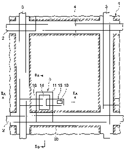
FIG. 1 shows a plan view of the principal
part of a thin film transistor panel in a liquid
crystal display device as a first embodiment of
the present invention. FIG. 2A shows a sectional
view taken along a line IIA-IIA in FIG. 1, and FIG.
2B shows a sectional view taken along a line IIB-
IIB in FIG. 1. The thin film transistor panel is
provided with a glass substrate 1.
First, a description is given by referring
to FIG. 1. Numerous scanning lines 2 and numerous
data lines 3 are formed on the top face side of the glass
substrate 1 to be extended in directions to cross with
CA 02562405 2006-10-03
WO 2006/093028 PCT/JP2006/303348
each other at right angles. A display element including
a thin film transistor 5 connected to one corresponding
scanning line 2 and one corresponding data line 3, and a
pixel electrode 4 electrically connected to the thin film
5 transistor 5 is arranged in each region enclosed by both
the lines 2 and 3. The regions are arranged in a matrix.
Here, with an object of clarifying FIG. 1, the edge
portions of the pixel electrodes 4 are hatched by oblique
short solid lines.
In this case, each of the square-like pixel
electrodes 4 is arranged in each of the square-like
regions enclosed by the scanning lines 2 and the data
lines 3 in the state in which the pixel electrode 4 is
positioned as near as possible to the scanning lines 2
and the, data lines 3. Each of the thin film transistors
5 is arranged on the under side in the lower left corner
part of each of the pixel electrodes 4 in FIG. 1, and
almost the whole part of the thin film transistor 5 is
covered by the pixel electrode 4.
Next, the concrete structure of the thin film
transistor panel is described by referring to FIGS. 2A
and 2B. The scanning lines 2, each made of a light
blocking metal film such as chromium or the like, are
formed at predetermined positions on the top face of the
glass substrate 1. Gate electrodes 11 are formed at
predetermined positions on the top faces of the scanning
CA 02562405 2006-10-03
WO 2006/093028 PCT/JP2006/303348
6
lines 2, and are severally formed in the neighborhood
of the scanning lines 2 on the top face of the glass
substrate 1 so as to cross with the scanning lines 2 at
right angles (see FIG. 1). That is, one end portion of
each of the gate electrodes 11 is formed on the top face
of each of the scanning lines 2.
In this case, the gate electrodes 11 are formed
with a transparent metal oxide containing n type or p
type impurities. As the transparent metal oxide, for
example, zinc oxide, magnesium zinc oxide, cadmium zinc
oxide and the like can be cited. As the n type
impurities, for example, phosphorus, arsenic, antimony
and the like can be cited. As the p type impurities, for
example, boron, aluminum, gallium, indium and the like
can be cited.
As the forming method of the gate electrodes 11 and
the scanning lines 2, a method of forming a film by a
sputtering method using a metal oxide film including the
n type or the p type impurities mentioned above as a
target to pattern the formed film by using a
photolithography technique is recommended. In
the respects of electric field mobility, the
stability of characteristics, and workability, the n type
metal oxide film is generally suitable. However, because
the n type metal oxide film is a depletion type metal
oxide film and the leakage current thereof is large, the
CA 02562405 2006-10-03
WO 2006/093028 PCT/JP2006/303348
7
p type metal oxide film can be also used in case of
regarding being low power consumption, but the use of the
p type metal oxide film does not. mean that the metal
oxide film to be used for the formation of the gate
electrodes 11 and the scanning lines 2 is limited to the
p type metal oxide film.
A gate insulating film 12 made of silicon nitride
is formed on the top face of the glass substrate 1 having
the scanning lines 2 and the gate electrodes 11 thereon.
Semiconductor thin films 13, which severally have a band
gap of 2.5 V or higher and are severally made of one of
the transparent and intrinsic metal oxides mentioned
above, are formed on the top face of the gate insulating
film 12 on the gate electrodes 11. Because the
semiconductor thin films 13 severally having a wide band
gap of 2.5 V or higher do not absorb any visible light,
the semiconductor thin films 13 do not leak any light,
and do not need light blocking consequently. Channel
protecting films 14, which are made of silicon nitride,
are formed at almost the central parts of the top faces
of the semiconductor thin films 13.
Each of the data lines 3 is formed between
corresponding two of the pixel electrodes 4 on the gate
insulating film 12. The width of each of the data lines
3 is narrower than the gap of the two pixel electrodes 4.
The data lines 3 are formed with a metal film having a
CA 02562405 2006-10-03
WO 2006/093028 PCT/JP2006/303348
8
light blocking property and a sufficiently small
resistance value such as aluminum, chromium or the like.
A source electrode 15 and a drain electrode 16,
both made of a transparent n type metal oxide, are formed
on both the sides of the top face of each of the channel
protecting films 14, and on the top face of a
corresponding semiconductor thin film 13 on both the
sides of the channel protecting film 14. The materials
of the metal oxide and the n type impurities are the same
as those in case of the gate electrodes 11. The drain
electrode 16 is formed to be extended so as to cross with
the corresponding data line 3 at right angles so that the
end of the extended portion is overlapped on the data
line 3 (see FIG. 1). The source electrodes 15 and the
drain electrodes 16 are formed by the method of forming a
film by the sputtering method using an n type metal oxide
film as a target to pattern the source electrodes 15 and
the drain electrodes 16 by using the photolithography
technique similarly to the case of forming the gate
electrodes 11.
Here, each of the thin film transistors 5 is
composed of the gate electrode 11, the gate insulating
film 12, the semiconductor thin film 13, the channel
protecting film 14, the sauce electrode 15 and the drain
electrode 16. In this case, because the gate electrode
11 is formed of the transparent p type metal oxide or the
CA 02562405 2006-10-03
WO 2006/093028 PCT/JP2006/303348
9
transparent n type metal oxide, and because the sauce
electrode 15 and the drain electrode 16 are formed of the
transparent n type metal oxide, the thin film transistor
has a structure which transmits light.
5 Overcoat films 17, each made of silicon nitride,
are formed on the top face of the gate insulating film 12
having the thin film transistors 5 and the data lines 3
thereon. Contact holes 18 are formed at the portions of
the overcoat films 17 corresponding to predetermined
positions of the source electrodes 15. Pixel electrodes
(electrodes for pixels) 4, which are made of a
transparent electroconductive material such as ITO, are
formed at predetermined positions of the overcoat films
17 to be electrically connected with the source
electrodes 15 through the contact holes 18. In this case,
each of the pixel electrodes 4 is formed to cover almost
the whole of each of the thin film transistors 5.
As described above, because in the thin film
transistor panel each of the thin film transistors 5 has
the structure transmitting light and almost the whole of
the thin film transistor 5 is covered with each of the
pixel electrodes 4, all the area of the pixel electrode 4
including the thin film transistor 5 is a transmitting
region, and the opening ratio of the pixel can be
enlarged. In this case, although light enters the
semiconductor thin film 13, which is made of the
CA 02562405 2006-10-03
WO 2006/093028 PCT/JP2006/303348
transparent.intrinsic metal oxide mentioned above, of the
thin film transistor 5, the semiconductor thin film 13
transmits the entered light as it is, and no problems are
caused consequently.
5 Moreover, in the thin film transistor panel,
because the scanning lines 2 and the data lines 3 are
formed with the light blocking metal film such as the
aluminum, the chromium or the like in place of a
transparent metal oxide including impurities, the light
10 leakage between the pixel electrodes 4 can be prevented,
and the resistance value can be made to be sufficiently
small.
(Second Embodiment)
FIG. 3 shows a plan view of the principal part of a
thin film transistor panel in a liquid crystal display
device as a second embodiment of the present invention.
FIG. 4A shows a sectional view taken along a line IVA-IVA
in FIG. 3, and FIG. 4B shows a sectional view taken along
a line IVB-IVB in FIG. 3. Also in this case, with an
object for clarifying FIG. 3, the edge portions of the
pixel electrodes 4 are hatched by oblique short solid
lines.
The thin film transistor panel is different from
the thin film transistor panel shown in FIGS. 1, 2A and
2B in that the overcoat films 17 are omitted and each of
the pixel electrodes 4 is formed with the n type metal
CA 02562405 2006-10-03
WO 2006/093028 PCT/JP2006/303348
11
oxide on one side of the top face of each of the channel
protecting films 14, on the top face of each of the
semiconductor thin films 13 on the external side of the
channel protecting film 14, and at each of predetermined
positions on the top face of the gate insulating film 12
to make a part of the pixel electrode 4 operate as a
source electrode.
For manufacturing the thin film transistor panel,
the method described with regard to the first embodiment
is used. That is, the scanning lines 2, each made of a
metal film having the light blocking property, and the
gate~electrodes 11, each made of a transparent p type or
n type metal oxide film, are formed on the top face of
the glass substrate 1. Next, the gate insulating film 12
is formed. On the gate insulating film 12, the
semiconductor thin films 13, each made of a transparent
intrinsic metal oxide, and the data lines 3, each made of
a metal film having the light blocking property, are
formed. The channel protecting films 14 are formed at
almost the central parts on the top faces of the
semiconductor thin films 13. Then, an n type metal oxide
film is formed by the sputtering method, and the drain
electrodes 16 and the pixel electrodes 4 are formed by
the photolithographic method. However, at this
time, the shapes of the pixel electrodes 4 are
made to be ones integrating each of the source
CA 02562405 2006-10-03
WO 2006/093028 PCT/JP2006/303348
12
electrodes and each of the pixel electrodes to be
one body.
In this case, because the pixel electrodes 4 are
formed on the same surfaces as those of the drain
electrodes 16, the planer shape of each of the pixel
electrodes 4 is made to be one cut off at the corner part
in the lower left of the pixel electrode in FIG. 3. But,
because at least a portion of the pixel electrode 4 which
functions as the source electrode, namely the portion
formed on the corresponding channel protecting film 14
and the corresponding semiconductor thin film 13, covers
a part of the corresponding gate electrode 11, the
overlapping part of the pixel electrode 4 and the gate
electrode 11 contributes to the opening ratio of the
pixel. Consequently, the opening ratio can be enlarged.
Moreover, the pixel electrodes 4 can be formed at the
same process as those of the drain electrodes 16, and it
is unnecessary to form the over coat films 17 and the
contact holes 18 to enable to reduce the number of
processes.
(Third Embodiment)
FIGS. 5A and 5B show the sectional views of the
principal part of an organic electroluminescence (EL)
display device as a third embodiment of the present
invention. In the organic EL display device, the same
constituent elements as those of the thin film transistor
CA 02562405 2006-10-03
WO 2006/093028 PCT/JP2006/303348
13
panel shown in FIGS. 2A and 2B are denoted by the same
reference marks as those in FIGS. 2A and 2B, and their
descriptions are omitted. In the organic EL display
device, light emitting portions made of the 'organic EL
are formed on the thin film transistors 5. That is, the
organic EL display device is configured as follows. Only
the portion of each of the thin film transistors 5 except
the corresponding source electrode 15 is covered by the
corresponding overcoat film 17. A corresponding anode
electrode (an electrode for the pixel) 21 is formed on
the source electrode 15, on a part of the overcoat film
17, and on the gate insulating film 12. A corresponding
partition wall 22 made of polyimide or the like is formed
at a predetermined position on the top face of the
overcoat film 17 and the gate insulating film 12. A
corresponding organic EL layer 23 is formed on the top
face of the anode electrode 21 between the partition wall
22 and a partition wall 22 in an adjacent pixel. A
cathode electrode 24 is formed on the top faces of the
organic EL layers 23 and the partition walls 22.
In this case, the anode electrode 21 is formed so
as to cover almost the whole portion of the thin film
transistor 5. Moreover, the anode electrode 21 is formed
with a transparent electroconductive material such as ITO
or the like, and the cathode electrode 24 is formed with
high reflexibility metal such as aluminum. In the
CA 02562405 2006-10-03
WO 2006/093028 PCT/JP2006/303348
14
configuration, because the light emitted from the organic
EL layer 23 is reflected by the cathode electrode 24,
which is formed on the organic EL layer 23, to be
launched to the side of the glass substrate 1, the
configuration is called as a bottom emission type. In
such a bottom emission type organic EL display device,
because the drain electrode 16, the source electrode 15,
the semiconductor thin film 13 and the gate electrode 11
are formed with the transparent metal oxide films, and
because the thin film transistor 5 transmits the light
which has been emitted from the organic EL layer 23 and
has been reflected by the cathode electrode 24, the whole
region of the thin film transistor 5 becomes a light
emitting region, and the opening ratio of the pixel can
be enlarged.
(Fourth Embodiment)
FIGS. 6A and 6B show the sectional views of
the principal part of an organic EL display
device as a fourth embodiment of the present
invention. Each pixel of the organic EL display
device is different from each pixel of the
organic EL display device shown in FIGS. 5A and
5B in that the overcoat film 17 is omitted, and
that the anode electrode 21 is formed with, for example,
the transparent metal oxide including n type impurities
on one side of the top face of the channel protecting
CA 02562405 2006-10-03
WO 2006/093028 PCT/JP2006/303348
film 14, on the top face of the semiconductor thin film
13 on the external side of the channel protecting film 14,
and at a predetermined position on the top face of the
gate insulating film.l2 to make the anode electrode 21
5 operate also as a source electrode.
In this case, predetermined corner parts of
the anode electrode 21, the organic EL layer 23
and the cathode electrode 24 are cut off
similarly to the case of cutting off the pixel
10 electrode 4 at the corner part in the lower left
of the pixel electrode 4 in FIG. 3 because the
anode electrode 21 is formed on the same surface
as that of the drain electrode 16.. However,
because at least the portion of the anode
15 electrode 21 which functions as the source
electrode, namely the portion formed on the
channel protecting film 14 and the semiconductor
thin film 13, covers a part of the gate electrode
11, the overlapping portion of the anode
electrode 21 and the gate electrode 11
contributes to the opening ratio of the pixel,
and consequently the opening ratio can be
enlarged. Moreover, the anode electrode 21 can
be formed at the same process as that of the
drain electrode 16, and consequently the number
of processes can be reduced.
CA 02562405 2006-10-03
WO 2006/093028 PCT/JP2006/303348
16
(Other Embodiments)
Although one end portion of each of the gate
electrodes 11 and. one end portion of each of the
drain electrodes 16, both made of the metal oxide
containing, for example, the n type impurities,
are formed on each top face of the corresponding
scanning line 2 and the corresponding data.line 3,
respectively, in, for example, FIGS. 1, 2A and 2B,
the present invention is not limited to such a
configuration. The metal oxide film containing,
for example, the n type impurities may be formed,
for example, on the whole of each top face of the
scanning line 2 and the data line 3. Moreover,
the scanning line 2 and the data line 3 may be
formed on the top face of each one end portion of
the gate electrode 11 and the drain electrode 16.
In this case, the metal oxide film including, for
example, the n type impurities may be formed on
the whole of each under surface of the scanning
line 2 and the data line 3.
Moreover, in the case of the organic EL display
panel, two thin film transistors may be formed in a pixel,
which is composed of a group of one of the anode
electrodes 21, one of the organic EL layers 23 and the
cathode electrode 24 (see, for example, JP 2004-171882A).
Moreover, three thin film transistors may be formed in
CA 02562405 2006-10-03
WO 2006/093028 PCT/JP2006/303348
17
one pixel (see, for example, JP 2003-195810A).
POSSIBILITY OF INDUSTRIAL UTILIZATION
As described above, according to the present
invention, because at least a part of the gate electrode
of a thin film transistor is covered by an electrode for
a pixel as the structure of the thin film transistor
which transmits light in each pixel, the overlapping
portion of the gate electrode of the thin film transistor
and the electrode for the pixel contributes to the
opening ratio of the pixel, and consequently the opening
ratio can be enlarged. The thin film transistor panel
according to the invention can be utilized suitably for
various types of display devices, e.g., an LC display
device, an EL display device or the like.