Note: Descriptions are shown in the official language in which they were submitted.
CA 02562747 2015-07-27
MASS SPECTROMETER
Field
The present invention relates to an ion detector, a mass
spectrometer, a method of detecting ions and a method of mass
spectrometry.
Background
Various different types of detectors for detecting and
recording individual electrons, ions or photons are known. A
particular type of an ion detector is known wherein ions impinge
upon one or more microchannel plates ("MCPs") causing secondary
electrons to be released and amplified. A pulse of electrons
emitted from a microchannel plate arrives at a collection anode
and is counted using a fast electronic event counter. Such ion
detectors are commonly used in Time of Flight ("TOF") mass
analysers in mass spectrometers for detecting and recording
individual ions and their arrival times.
It is known that the maximum count rate for such known ion
detectors can be increased by using multiple collection anodes
each with its own fast electronic event counter rather than a
single collection anode. Ion detectors employing multiple
collection anodes are used, for example, in Time of Flight mass
analysers to extend the dynamic range of the mass analyser. The
collection anodes are arranged to collect and record different
fractions or groups of the secondary electron pulses produced
due to ions arriving at the input to the detector system. Each
collection anode is attached to its own separate amplifier,
discriminator and Time to Digital Converter (TDC).
Once the ion arrival rate at the input of a known electron
multiplier detector system exceeds a certain limit then the
signal recorded from the larger of the two collection anodes
will become increasingly inaccurate. Accordingly, the ion
arrival event counter will begin to miss counts. However, the
signal recorded from the smaller collection anode arranged to
detect and record the smaller fraction of secondary electron
pulses will continue to count all the ions arriving at the
corresponding input area of the microchannel plate. If the
ratio between the fractions of ion arrival events recorded on
the different collection anodes is known, then the overall ion
arrival rate can be calculated. Accordingly, the dynamic range
for quantification of the arriving ion current can be extended.
CA 02562747 2006-10-12
WO 2005/104178 PCT/GB2005/001585
- 2 -
In a Time of Flight mass spectrometer missed ion counts
will lead to a shift in the recorded ion arrival distribution
for ions having a specific mass to charge ratio. This will lead
to a shift in the measured mean arrival time of the ions and
consequently an error in the determination of their mass to
charge ratio will be introduced. If the dynamic range of the
ion detector is increased then the accuracy of both the
quantification of the ion signal and the determination of the
, mass to charge ratio of the corresponding ions may be increased.
It is contemplated that the dynamic range of an ion
counting detector could be improved by providing a mask to
attenuate the number of secondary electron pulses arriving at
one of the collection anodes. It is contemplated that the mask
could be positioned either downstream of the final microchannel
plate to prevent some secondary electrons from impinging upon
one of the collection anodes or alternatively the mask could be
provided upstream of the first microchannel plate in order to
reduce the intensity of ions impinging upon the microchannel
plates. In any event, the two collection anodes are arranged to
collect different fractions of the secondary electron pulses
emitted from the microchannel plates.
One problem with these contemplated arrangements is that
=
for each ion arrival the resulting cloud of secondary electrons
arriving at the collection anodes will be quite broad. If an
ion arrives at a microchannel plate at a position close to the
edge of one of the collection anodes in a multiple anode
detector system then it is likely that only some or a portion of
the secondary electrons generated by an ion arrival will
subsequently strike the particular collection anode. However,
the number of electrons striking a collection anode will largely
determine whether or not an ion arrival is detected and counted.
The likelihood of an ion arrival event being recorded will
therefore depend upon the position of the ion when it strikes
the detector, the electron amplification factor in an electron
multiplier, the proportion of electrons in an resultant electron
cloud which strikes a collection anode, the amplifier gain and
the event counter discriminator level.
The electron amplification factor in an electron
multiplier varies from event to event usually according to a
CA 02562747 2006-10-12
WO 2005/104178 PCT/GB2005/001585
- 3 -
Gaussian distribution. An ion counting system is normally
designed such that the normal (Gaussion) variation in the
electron amplification factor is not sufficient to significantly
affect the number of ions counted, whilst any noise in the
system is not sufficient to trigger superfluous counts.
However, it will be apparent that when ions arrive at a position
on the ion detector that corresponds to a boundary of a
collection anode then it may not be so cleanly differentiated
from noise and the number of counts due to ions which arrive at
such positions on the ion detector will vary directly with the
settings of the detector system.
An additional significant problem is that, if two
collection anodes are arranged in sufficiently close proximity
to one another, then a cloud of secondary electrons produced by
a single ion arrival at the input of an ion detector may be
partially incident upon'both the collection anodes. This may
result in either the ion arrival event not being counted, or
else the ion arrival event may be counted once or twice by the
tfAio collection anodes. The extent to which this may happen will
vary directly with the settings of the detector system.
The inaccuracies resulting from this effect would be
particularly significant for a collection anode arranged to
record the smaller fraction of secondary electrons. In some
designs, the smaller collection anode may be, for example, one
tenth or one hundredth of the area of the larger collection
anode. The significance of this error therefore becomes
correspondingly greater the smaller the relative area of the
smallest collection anode becomes. Furthermore, in some designs
of ion detector a collection anode may have a very large edge or
boundary relative to its area. For example, one collection
anode may comprise a large plate whilst another collection anode
may comprise a fine wire positioned in frorit of the large plate.
The fine wire collection anode will have a very large boundary
in proportion to its area. Accordingly, the ion detector may
suffer from significant errors in the ion count rate recorded by
the smaller wire collection anode. This error will be present
in the determination of the overall ion count rate for the
situation when the overall ion count rate is too high to be
accurately recorded on the larger anode.
CA 02562747 2006-10-12
WO 2005/104178 PCT/GB2005/001585
- 4 -
A particular problem associated with ions arriving at a
position corresponding to the boundary between collection anodes
is that of shared signals. Some ions may produce electron
clouds that strike more than one collection anode. These shared
electron clouds will produce smaller signals on each separate
collection anode and hence neither may be large enough to be
counted.
It is contemplated that a mask may be provided after the
final microchannel plate and before the collection anode with
the intention of blocking those electron clouds that would
otherwise be shared between two collection anodes from reaching
either collection anode. However, such an arrangement suffers
from the problem that only a part or portion of an electron
cloud may strike a particular collection anode. Since the
intensity of the cloud of electrons striking the collection
anode is reduced this may or may not be sufficient to be
registered as an ion arrival event. This will depend on the
electron amplification factor in the electron multiplier, the
proportion of the electron cloud that strikes the collection
anode, the amplifier gain and the detector discriminator level.
The proportion of ions arriving at a position near the
edge of the mask that will be detected will vary directly with
the settings of the detector system. For a small anode with a
large boundary, such as a fine wire collection anode, this may
introduce a significant error to the number of ions counted.
It is contemplated that a mask may be provided upstream of
the front face of the first microchannel plate with the
intention of blocking those ions from reaching the ion detector
that would otherwise yield a cloud of electrons that would be
shared between two collection anodes. Such a contemplated
arrangement does not suffer from the same problems as described
above when a mask is provided downstream of the final
microchannel plate detector. However, such an arrangement would
require a mask to be mounted in front of the front surface of
the first microchannel plate and would cause a number of
different problems.
Firstly, if such a detector were to be used in a Time of
Flight mass spectrometer then some ions having a certain mass to
charge ratio will strike the detector surface before others
CA 02562747 2015-07-27
- 5 -
depending upon whether they strike the microchannel plate input
face or the mask. Ions striking the edge of the mask may also
cause secondary electrons to be released which will then be
amplified by the microchannel plates and hence will be
subsequently detected giving rise to ghost peaks in the
resulting mass spectrum.
Secondly, in some designs of ion detector, such as in post
acceleration ion detectors, ions are still being accelerated as
they approach the ion detector. If the front face of the
microchannel plate arranged to receive ions is not perfectly
flat then the accelerating electric field will also not be
perfectly uniform. As a result if a mask is provided on the
front face of the first microchannel plate then some ions may be
accelerated differently to others causing some ions to be
deflected and hence arriving at the ion detector at slightly
different times. This will result in the broadening of mass
peaks in a resulting mass spectrum.
Thirdly, any mask which is intentionally arranged so as to
be bombarded by ions may become coated over a period of time
with material that may be insulating. As a result, the mask may
begin to hold a charge thereby further disturbing the flight
path and arrival times of ions. The mask may also be bombarded
by incoming ions causing sputtering of secondary atoms and ions,
some of which may be subsequently detected by the detector
giving rise to ghost peaks in the resulting mass spectrum.
Summary
According to an aspect of the present invention there is
provided an ion detector comprising:
a first microchannel plate device;
a second microchannel plate device;
a mask or shield provided intermediate between the first
microchannel plate device and second microchannel plate device;
and
at least a first collection anode having a first active
electron detecting area or size and a second separate collection
anode having a second different active electron detecting area
or size arranged downstream of the second microchannel plate
device.
According to an embodiment, the second active electron
detecting area or size is equal to a percentage x of the first
CA 02562747 2006-10-12
WO 2005/104178 PCT/GB2005/001585
- 6 -
active electron detecting area or size, wherein x is selected
from the group consisting of: (i) < 0.2 %; (ii) 0.2-0.3 %; (iii)
0.3-0.4 %; (iv) 0.4-0.5 %; (v) 0.5-0.6 %; (vi) 0.6-0.7 %; (vii)
0.7-0.8 %; (viii) 0.8-0.9 %; (ix) 0.9-1.0 %; (x) 1-10 %; (xi)
10-20 %; (xii) 20-30 %; (xiii) 30-40 %; (xiv) 40-50 %; (xv) 50-
60 %; (xvi) 60-70 %; (xvii) 70-80 %; (xviii) 80-90 %; (xix) 90-
100%.
The first microchannel plate device may comprise one, two
or more than two microchannel plates. Similarly, the second
microchannel plate device may comprise one, two or more than two
microchannel plates.
The mask or shield is preferably arranged to block,
attenuate, at least partially attenuate or divert electrons
emitted from the first microchannel plate device. Preferably,
the mask or shield substantially prevents electrons exiting from
or emerging from the first microchannel plate device and/or from
impinging upon or arriving at the second microchannel plate
device. According to an embodiment the mask or shield is
arranged such that at least some ions arriving at the first
microchannel plate device at certain locations or positions on
the first microchannel plate device are either: (a)
substantially prevented from subsequently causing a cloud of
secondary electrons to be emitted from the second microchannel
plate device; or (b) subsequently cause a cloud of secondary
electrons to be emitted from the second microchannel plate
device which either substantially impinge upon the first
collection anode or upon the second collection anode but wherein
the cloud of secondary electrons emitted from the second
microchannel plate device do not substantially impinge
simultaneously upon both the first collection anode and the
second collection anode.
According to an embodiment the mask or shield is arranged
such that ions.arriving at the first microchannel plate device
do not substantially result in a cloud of secondary electrons
being produced which impinges simultaneously upon both the first
collection anode and the second collection anode. Preferably,
the mask or shield is arranged such that ions arriving at the
first microchannel plate device result in a cloud of secondary
electrons which impinges either upon the first collection anode
CA 02562747 2006-10-12
WO 2005/104178 PCT/GB2005/001585
- 7 -
or upon the second collection anode but not upon both the first
and second collection anodes simultaneously.
According to an embodiment the mask or shield has a
thickness selected from the group consisting of: (i) < 1 pm;
(ii) 1-5 pm; (iii) 5-10 pm; (iv) 10-15 pm; (v) 15-20 gm; (vi)
20-25 pm; (vii) 25-30 pm; (viii) 30-35 pm; (ix) 35-40 pm; (x)
40-45 pm; (xi) 45-50 pm; (xii) 50-55 pm; (xiii) 55-60 pm; (xiv)
60-65 gm; (xv) 65-70 pm; (xvi) 70-75 pm; (xvii) 75-80 pm;
(xviii) 80-85 pm; (xix) 85-90 pm; (xx) 90-95 gm; (xxi) 95-100
pm; and (xxii) > 100 pm.
Preferably, at least the front face of the first
microchannel plate device is maintained, in use, at a voltage or
potential selected from the group consisting of: (i) 0 V; (ii) +
0-10 V; (iii) 10-100 V; (iv) 100-500 V; (v) 500-1000 V;
(vi) 1-2 kV; (vii) 2-3 kV; (viii) 3-4 kV; (ix) 4-5 kV;
(x) 5-6 kV; (xi) 6-7 kV; (xii) 7-8 kV; (xiii) 8-9 kV;
(xiv) 9-10 kV; and (xv) > 10 kV. Preferably, at least the
rear face of the first microchannel plate device is maintained,
in use, at a voltage or potential selected from the group
consisting of: (i) 0 V; (ii) 0-10 V; (iii) 10-100 V; (iv)
100-500 V; (v) 500-1000 V; (vi) 1-2 kV; (vii) 2-3 kV;
(viii) 3-4 kV; (ix) 4-5 kV; (x) 5-6 kV; (xi) 6-7 kV;
(xii) 7-8 kV; (xiii) 8-9 kV; (xiv) 9-10 kV; and (xv) >
10 kV. Preferably, a potential difference is maintained, in
use, across the first microchannel plate device selected from
the group consisting of: (i) 0 V; (ii) 0-10 V; (iii) 10-100
V; (iv) 100-500 V; (v) 500-1000 V; (vi) 1-2 kV; (vii) 2-
3 kV; (viii) 3-4 kV; (ix) 4-5 kV; (x) 5-6 kV; (xi) 6-7
kV; (xii) 7-8 kV; (xiii) 8-9 kV; (xiv) 9-10 kV; and (xv) >
10 kV.
According to an embodiment at least the front face of the
mask or shield is maintained, in use, at a voltage or potential
selected from the group consisting of: (i) 0 V; (ii) 0-10 V;
(iii) 10-100 V; (iv) 100-500 V; (v) 500-1000 V; (vi) 1-2
kV; (vii) 2-3 kV; (viii) 3-4 kV; (ix) 4-5 kV; (x) 5-6
kV; (xi) 6-7 kV; (xii) 7-8 kV; (xiii) 8-9 kV; (xiv) 9-10
kV; and (xv) > 10 kV. Preferably, at least the rear face of
the mask or shield is maintained, in use, at a voltage or
potential selected from the group consisting of: (i) 0 V; (ii)
CA 02562747 2006-10-12
WO 2005/104178 PCT/GB2005/001585
-8--
0-10 V; (iii) 10-100 V; (iv) 100-500 V; (v) 500-1000 V;
(vi) 1-2 kV; (vii)' 2-3 kV; (viii) 3-4 kV; (ix) 4-5 kV;
(x) 5-6 kV; (xi) 6-7 kV; (xii) 7-8 kV; (xiii) 8-9 kV;
(xiv) 9-10 kV; and (xv) > 10 kV. Preferably, a potential
difference is maintained, in use, across the mask or shield
selected from the group consisting of: (i) 0 V; (ii) 0-10 V;
(iii) 10-100 V; (iv) 100-500 V; (v) 500-1000 V; (vi) + 1-2
kV; (vii) 2-3 kV; (viii) 3-4 kV; (ix) 4-5 kV; (x) 5-6
kV; (xi) 6-7 kV; (xii) 7-8 kV; (xiii) 8-9 kV; (xiv) 9-10
kV; and (xv) > 10 kV.
According to an embodiment at least the front face of the
second microchannel plate device is maintained, in use, at a
voltage or potential selected from the group consisting of: (i)
0 V; (ii) 0-10 V; (iii) 10-100 V; (iv) 100-500 V; (v)
500-1000 V; (vi) 1-2 kV; (vii) 2-3 kV; (viii) 3-4 kV; (ix)
4-5 kV; (x) 5-6 kV; (xi) 6-7 kV; (xii) 7-8 kV; (xiii)
8-9 kV; (xiv) 9-10 kV; and (xv) > 10 kV. Preferably, the
rear face of the second microchannel plate device is maintained,
in use, at a voltage or potential selected from the group
consisting of: (i) 0 V; (ii) 0-10 V; (iii) 10-100 V; (iv)
100-500 V; (v) 500-1000 V; (vi) 1-2 kV; (vii) 2-3 kV;
(viii) 3-4 kV; (ix) 4-5 kV; (x) 5-6 kV; (xi) '6-7 kV;
(xii) 7-8 kV; (xiii) 8-9 kV; (xiv) 9-10 kV; and (xv) >
10 kV. Preferably, a potential difference is maintained, in
use, across the second microchannel plate device selected from
the group consisting of: (i) 0 V; (ii) 0-10 V; (iii) 10-100
V; (iv) 100-500 V; (v) 500-1000 V; (vi) 1-2 kV; (vii) 2-
3 kV; (viii) 3-4 kV; (ix) 4-5 kV; (x) 5-6 kV; (xi) 6-7
kV; (xii) 7-8 kV; (xiii) 8-9 kV; (xiv) 9-10 kV; and (xv) >
10 kV.
According to an embodiment a potential difference is
maintained, in use, between the rear surface of the first
microchannel plate device and the front surface of the mask or
shield selected from the group consisting of: (i) 0 V; (ii) 0-
10 V; (iii) 10-100 V; (iv) 100-500 V; (v) 500-1000 V; (vi)
1-2 kV; (vii) 2-3 kV; (viii) 3-4 kV; (ix) 4-5 kV; (x)
5-6 kV; (xi) 6-7 kV; (xii) 7-8 kV; (xiii) 8-9 kV; (xiv)
9-10 kV; and (xv) > 10 kV. Similarly, according to an
embodiment a potential difference is maintained, in use, between
CA 02562747 2006-10-12
WO 2005/104178 PCT/GB2005/001585
- 9 -
the rear surface of the mask or shield and the front surface of
the second microchannel plate device selected from the group
consisting of: (i) 0 V; (ii) 0-10 V; (iii) 10-100 V; (iv) +
100-500 V; (v) 500-1000 V; (vi) 1-2 kV; (vii) 2-3 kV;
(viii) 3-4 kV; (ix) 4-5 kV; (x) 5-6 kV; (xi) 6-7 kV;
(xii) 7-8 kV; (xiii) 8-9 kV; (xiv) 9-10 kV; and (xv) > +
kV.
The mask or shield is preferably attached to or otherwise
provided on a rear surface of the first microchannel plate
10 device. The mask or shield is preferably attached to or
otherwise provided on a front surface of the second microchannel
plate device. According to an embodiment the mask or shield is
attached to or otherwise provided on a rear surface of the first
microchannel plate device and is attached to or otherwise
provided on a front surface of the second microchannel plate
device.
The mask or shield preferably comprises a material
selected from the group consisting of: (i) a metal; (ii) a
plastic; (iii) a ceramic; (iv) a conductor; (v) an insulator;
(vi) a semiconductor; (vii) a thin film; (viii) an organic
layer; (ix) an inorganic layer; (x) a polyimide layer; (xi) a
thermoplastic layer; and (xii) Kapton (RTM).
The first microchannel plate device preferably comprises a
front surface upon which ions are received in use and a rear
surface from which electrons are emitted in use and wherein the
second microchannel plate device comprises a front surface upon
which electrons emitted from the first microchannel plate device
are received in use and a rear surface from which electrons are
emitted in use.
The separation between the rear surface of the first
microchannel plate device and the front surface of the second
microchannel plate device is preferably selected from the group
consisting of: (i) < 1 pm; (ii) 1-5 pm; (iii) 5-10 pm; (iv) 10-
15 gm; (v) 15-20 pm; (vi) 20-25 pm; (vii) 25-30 pm; (viii) 30-35
pm; (ix) 35-40 pm; (x) 40-45 pm; (xi) 45-50 pm; (xii) 50-55 pm;
(xiii) 55-60 pm; (xiv) 60-65 pm; (xv) 65-70 pm; (xvi) 70-75 pm;
(xvii) 75-80 pm; (xviii) 80-85 pm; (xix) 85-90 pm; (xx) 90-95
pm; (xxi) 95-100 pm; and (xxii) > 100 pm.
CA 02562747 2006-10-12
WO 2005/104178 PCT/GB2005/001585
- 10 -
According to an embodiment the separation between the rear
surface of the second microchannel plate device and a front
surface of the first collection anode is selected from the group
consisting of: (i) < 1 pm; (ii) 1-10 pm; (iii) 10-20 pm; (iv)
20-30 pm; (v) 30-40 pm; (vi) 40-50 pm; (vii) 50-60 gm; (viii)
60-70 pm; (ix) 70-80 pm; (x) 80-90 pm; (xi) 90-100 pm; (xii)
100-120 pm; (xiii) 120-140 pm; (xiv) 140-160 pm; (xv) 160-180
pm; (xvi) 180-200 pm; (xvii) 200-250 pm; (xviii) 250-300 pm;
(xix) 300-350 pm; (xx) 350-400 pm; (xxi) 400-450 pm; (xxii) 450-
500 pm; and (xxiii) > 500 pm.
According to an embodiment the separation between the rear
surface of the second microchannel plate device and a front
surface of the second collection anode is selected from the
group consisting of: (i) < 1 pm; (ii) 1-10 gm; (iii) 10-20 gm;
(iv) 20-30 pm; (v) 30-40 pm; (vi) 40-50 pm; (vii) 50-60 pm;
(viii) 60-70 pm; (ix) 70-80 pm; (x) 80-90 pm; (xi) 90-100 pm;
(xii) 100-120 pm; (xiii) 120-140 pm; (xiv) 140-160 pm; (xv) 160-
180 pm; (xvi) 180-200 pm; (xvii) 200-250 pm; (xviii) 250-300 gm;
(xix) 300-350 pm; (xx) 350-400 pm; (xxi) 400-450 pm; (xxii) 450-
500 pm; and (xxiii) > 500 pm.
Preferably, the first collection anode is substantially
larger than the second collection anode. The first collection
anode preferably has a first active electron detecting area and
the second collection anode has a second active electron
detecting area, wherein the ratio of the first active electron
detecting area to the second active electron detecting area is
selected from the group consisting of: (i) < 1; (ii) 1-1.5;
(iii) 1.5-2.0; (iv) 2-3; (v) 3-4; (vi) 4-5; (vii) 5-6; (viii) 6-
7; (ix) 7-8; (x) 8-9; (xi) 9-10; (xii) 10-15; (xiii) 15-20;
(xiv) 20-25; (xv) 25-30; (xvi) 30-35; (xvii) 35-40; (xviii) 40-
45; (xix) 45-50; (xx) 50-60; (xxi) 60-70; (xxii) 70-80; (xxiii)
80-90; (xxiv) 90-100; (xxv) 100-150; (xxvi) 150-200; (xxvii)
200-250; (xxviii) 250-300; (xxix) 300-350; (xxx) 350-400; (xxxi)
400-450; (xxxii) 450-500; and (xxxiii) > 500.
According to an embodiment the first and second collection
anodes are substantially co-planar. According to a less
preferred embodiment the first and second collection anodes are
not substantially co-planar.
CA 02562747 2006-10-12
WO 2005/104178 PCT/GB2005/001585
- 11 -
Preferably, the first collection anode substantially
encloses, surrounds or envelopes the second collection anode.
According to an embodiment the second collection anode is
provided in a slot, channel, slit, aperture or window within the
first collection anode or formed by the first collection anode.
Preferably, the size of the slot, channel, slit, aperture or
window within the first collection anode or formed by the first
collection anode is substantially greater or larger than the
size, area, diameter, length or width of the second collection
anode.
The first collection anode preferably comprises one or
more collection anodes. The first collection anode may comprise
an array of collection anodes. The second collection anode
preferably comprises one or more collection anodes. The second
collection anode may comprise an array of collection anodes.
According to an embodiment the ion detector preferably
comprises one or more Time to Digital Converters ("TDC")
connected to the first collection anode. According to an
embodiment the ion detector preferably one or more Analogue to
Digital Converters ("ADC") connected to the first collection
anode.
According to an embodiment the ion detector preferably
comprises one or more Time to Digital Converters ("TDC")
connected to the second collection anode. According to an
embodiment the ion detector preferably one or more Analogue to
Digital Converters ("ADC") connected to the second collection
anode.
According to an aspect of the present invention there is
provided an analytical instrument comprising an ion detector as
described.
According to an aspect of the present invention there is
provided a mass analyser comprising an ion detector as described
above.
According to an aspect of the present invention there is
provided a mass spectrometer comprising an ion detector as
described above.
The mass spectrometer preferably further comprises a mass
analyser. The mass analyser is preferably selected from the
group consisting of: (i) an orthogonal acceleration Time of
CA 02562747 2006-10-12
WO 2005/104178 PCT/GB2005/001585
- 12 -
Flight mass analyser; (ii) an axial acceleration Time of Flight
mass analyser; (iii) a Paul 3D quadrupole ion trap mass
analyser; (iv) a 2D or linear quadrupole ion trap mass analyser;
(v) a Fourier Transform Ion Cyclotron Resonance mass analyser;
(vi) a magnetic sector mass analyser; (vii) a quadrupole mass
analyser; and (viii) a Penning trap mass analyser.
The mass spectrometer or other analytical instrument
preferably further comprises an ion source. The ion source may
be either a pulsed ion source or a substantially continuous ion
source. The ion source is preferably selected from the group
consisting of: (i) an Electrospray ionisation ("ESI") ion
source; (ii) an Atmospheric Pressure Photo Ionisation ("APPI")
ion source; (iii) an Atmospheric Pressure Chemical Ionisation
("APCI") ion source; (iv) a Matrix Assisted Laser Desorption
Ionisation ("MALDI") ion source; (v) a Laser Desorption
Ionisation ("LDI") ion source; (vi) an Atmospheric Pressure
Ionisation ("API") ion source; (vii) a Desorption Ionisation on
Silicon ("DIOS") ion source; (viii) an Electron Impact ("El")
ion source; (ix) a Chemical Ionisation ("CI") ion source; (x) a
Field Ionisation ("Fl") ion source; (xi) a Field Desorption
("FD") ion source; (xii) an Inductively Coupled Plasma ("ICP")
ion source; (xiii) a Fast Atom Bombardment ("FAB") ion source;
(xiv) a Liquid Secondary Ion Mass Spectrometry ("LSIMS") ion
source; (xv) a Desorption Electrospray Ionisation ("DESI") ion
source; and (xvi) a Nickel-63 radioactive ion source.
According to another aspect of the present invention there
is provided a method of detecting ions comprising:
directing ions on to an ion detector comprising a first
microchannel plate device, a second microchannel plate device
and a mask or shield provided intermediate between the first
microchannel plate device and second microchannel plate device;
detecting electrons emitted from the second microchannel
plate device using at least a first collection anode and a
second separate collection anode, the first collection anode
having a first active electron detecting area or size and the
second collection anode having a second different active
electron detecting area or size, and the first collection anode
and the second collection anode arranged downstream of the
second microchannel plate device.
CA 02562747 2006-10-12
W02005/104178 PCT/GB2005/001585
- 13 -
According to an aspect of the present invention there is
provided a method of mass spectrometry comprising the method of
detecting ions as described above.
According to an aspect of the invention there is provided
an ion detector comprising:
a first microchannel plate device;
a second microchannel plate device; and
a mask or shield provided intermediate between the first
microchannel plate device and second microchannel plate device,
wherein the separation between the first microchannel plate
device and second microchannel plate device is 50 pm.
According to an aspect of the invention there is provided
an ion detector comprising:
a first microchannel plate device;
a second microchannel plate device;
a mask or shield provided intermediate between the first
microchannel plate device and second microchannel plate device,
wherein the mask or shield comprises an insulator.
According to an embodiment the mask or shield comprises a
material selected from the group consisting of: (i) a plastic;
(ii) a ceramic; (iii) a thin film; (iv) an organic layer; (v) an
inorganic layer; (vi) a polyimide layer; (vii) a thermoplastic
layer; and (viii) Kapton (RTM).
According to an aspect of the invention there is provided
an ion detector comprising:
a first microchannel plate device;
a second microchannel plate device; and
a mask or shield provided intermediate between the first
microchannel plate device and second microchannel plate device.
The preferred embodiment relates to a microchannel plate
detector assembly comprising two or more microchannel plates and
two or more collection anodes. A mask is placed between the two
microchannel plates such that all the electrons in an electron
cloud emerging from the second downstream microchannel plate,
due to an ion striking the first upstream microchannel plate
only strike one of the two collection anodes. The separation
between the microchannel plates is preferably 50 gra or less.
CA 02562747 2015-07-27
- 14 -
The collection anodes preferably have unequal electron
detecting areas although according to a less preferred
embodiment the two or more collection anodes may have
substantially the same area. The mask shape and size is
preferably such that it at least masks the boundary between two
collection anodes so that an ion incident on the input face of a
first microchannel plate does not result in an electron cloud
emerging from the second microchannel plate wherein only some of
the electrons strike one collection anode. In a preferred
embodiment the mask comprises an insulator.
In a preferred embodiment one or more of the collection
anodes in the ion detector are preferably used in conjunction
with an amplifier, a discriminator and a fast event counter for
the purpose of counting ions.
The preferred ion detector is preferably used in a Time of
Flight mass spectrometer incorporating a Time to Digital
Converter (TDC) to detect ions and record their arrival times.
The preferred ion detector preferably exhibits an extended
dynamic range for quantification applications and/or mass
measurement applications.
Brief Description of the Drawings
Various embodiments of the present invention will now be
described, by way of example only, together with other
arrangements given for illustrative purposes only and with
reference to the accompanying drawings in which:
Fig. 1 shows a known ion detector comprising a pair of
microchannel plates and a single collection anode;
Fig. 2 shows another known ion detector comprising a pair
of microchannel plate plates and two different sized collection
anodes arranged to collect different fractions of secondary
electrons emitted from the second rearmost microchannel plate;
Fig. 3 shows in greater detail the arrangement shown in
Fig. 2 and illustrates how in the known arrangement an ion
arriving at the ion detector may result in a cloud of secondary
electrons being emitted from the second microchannel plate which
impinges across both collection anodes;
Fig. 4A illustrates a channel in the first microchannel
plate activated by an ion arriving at the first microchannel
plate and Fig. 4B shows the corresponding channels energised in
CA 02562747 2015-07-27
. .
- 15 -
the second microchannel plate due to a cloud of electrons being
emitted from the first microchannel plate;
Fig. 5 shows an arrangement wherein a mask is provided on
the rear surface of the second microchannel plate;
Fig. 6A shows in greater detail how with the arrangement
shown in Fig. 5 an ion arriving at the first microchannel plate
causes a cloud of electrons to be emitted from the second
microchannel plate and Fig. 6B shows in greater detail how an
ion arriving at a different position on the first microchannel
plate in the arrangement shown in Fig. 5 causes secondary
electrons to be produced with the second microchannel plate but
only some of these electrons are emitted from the second
microchannel plate due to being blocked by the mask;
Fig. 7 shows an arrangement wherein a mask is provided on
the front surface or face of the first microchannel plate;
Fig. 8 shows a preferred embodiment of the present
invention wherein a mask is provided between the two
microchannel plates; and
Fig. 9 shows in greater detail how the mask according to
the preferred embodiment as shown in Fig. 8 prevents a cloud of
secondary electrons from being emitted from the second
microchannel plate which either impinges upon two collection
anodes or which can vary in intensity.
Description
A known microchannel plate ion detector is shown in Fig.
1. Such an ion detector may be in incorporated in a Time of
Flight mass spectrometer. Ions I are arranged to fall incident
upon the input face or front surface of a stack of two
microchannel plates 2a,2b. Secondary electrons are emitted from
the first microchannel plate 2a and are subsequently amplified
by the second microchannel plate 2b which is arranged downstream
of the first microchannel plate.
Pulses of secondary electrons or clouds of secondary
electrons exit or emerge from the second microchannel plate 2b
and strike the single collection anode 3. The pulse of
secondary electrons received by the collection anode 3 is then
amplified and subsequently recorded using a Time to Digital
Converter ("TDC") connected to the collection anode 3 at
location 4.
CA 02562747 2006-10-12
WO 2005/104178 PCT/GB2005/001585
- 16 -
Fig. 1 in particular illustrates a single instance in time
wherein ten ions arrive substantially simultaneously at the ion
detector. However, although ten ions arrive at the ion detector
the Time to Digital Converter connected to the single collection
anode 3 will only record a single event or ion arrival event.
It is for this reason that improved ion detectors are
known comprising two collection anodes. Fig. 2 illustrates such
a known ion detector which comprises two separate collection
anodes 5,6 having unequal areas. In the particular example
shown in Fig. 2 the first larger collection anode 5 collects
electron pulses resulting from 90% of the ions arriving at the
input face of the first microchannel plate 2a. Therefore, 90%
of the ions 1 arriving at the first microchannel plate 2a will
yield electron clouds which will strike the larger collection
anode 5 whilst only 10% of the ions 1 arriving at the first
microchannel plate will yield electron clouds which will strike
the smaller second collection anode 6.
A first Time to Digital Converter 5' is shown connected to
the larger collection anode 5 and will only record one ion
arrival event. However, a second Time to Digital Converter 6'
is shown connected to the smaller collection anode 6 and will in
addition record one ion arrival event.
Over many measurements the first Time to Digital Converter
5' may persistently record one event whereas the second Time to
Digital Converter 6' may sometimes record no event and sometimes
record one event.
If the output from the first Time to Digital Converter 5'
is recognised as being in error due, for example, to showing
signs of being saturated, then the signal recorded by the second
Time to Digital Converter 6' may then be used to estimate the
total signal arriving at the ion detector if the ratio of the
collection fractions for the two collection anodes 5,6 is known.
Therefore using two different sized collection anodes 5,6 allows
the dynamic range of the ion detector to be increased.
Fig. 3 shows in greater detail the known ion detector as
shown in Fig. 2. In particular, Fig. 3 shows the electron
clouds emitted from the first and second microchannel plates
2a,2b. Fig. 3 illustrates how an electron cloud emitted from
the first microchannel plate 2a spreads out and has a larger
CA 02562747 2006-10-12
WO 2005/104178
PCT/GB2005/001585
- 17 -
footprint or area on the input or incident surface of the second
microchannel plate 2b. Fig. 3 also illustrates how in a similar
manner electron clouds emitted from the exit surface of the
second microchannel plate 2b spread out and may impinge on the
first collection anode 5 and/or the second collection anode 6.
The diameter Dc of an electron cloud emerging from a
single channel of a microchannel plate at a distance S from the
exit face of that microchannel plate is given by:
= c1+4xSxsin0xcos0xE x 1+ Vb
Dc
1
Vb Ex cos 0 2
where:
0 = tan-1(¨d`
1 e
and wherein E is the mean exit energy of electrons leaving the
microchannel plate, S is the distance from the exit face of the
microchannel plate, Vb is the voltage difference across the
distance S, d is the diameter of a single microchannel plate
channel and p is the depth of penetration of the electrode
material into the microchannel plate channels at the exit of the
microchannel plate (end spoiling).
In order to further illustrate the arrangement shown in
Fig. 3, a stack of two microchannel plates can be considered.
The two microchannel plates can be considered provided in a
chevron arrangement in which individual channel diameters d are
10 pm, the end spoiling p is 10 rim, the channel pitch is 12 pm
and the inter-plate gap is 25 Rm. A microchannel plate
operating plate bias of 1000 V per plate may be assumed and the
mean energy E of electrons leaving the microchannel plate may be
determined as being approximately 35 eV.
For a single ion arriving at the input face of the first
microchannel plate 2a shown in Fig. 3, the resulting electron
cloud exiting the first microchannel plate 2a will have spread
to a diameter of approximately 60 pm upon striking the input
face of the second microchannel plate 2b. This corresponds to
illuminating approximately 23 channels of the second
CA 02562747 2006-10-12
WO 2005/104178 PCT/GB2005/001585
- 18 -
microchannel plate 2b. This is illustrated further in Figs. 4A
and 4B.
Fig. 4A shows the first microchannel plate 2a with a
single channel (shown shaded) being energised by the arrival of
an ion. Fig. 4B shows the second microchannel plate 2b and
those channels energised (shown shaded) by secondary electrons
exiting from the single channel in the first microchannel plate
2a diverging so as to illuminate a greater number of channels in
the second microchannel plate 2b.
If the gap between the exit face of the second
microchannel plate 2b and the first and second collection anodes
5,6 is taken to be 0.5 mm, and the bias voltage between the exit
face of the second microchannel plate 2b and the first and
second collection anodes 5,6 is set at 100 V then the diameter
of the cloud of electrons from each channel of the second
microchannel plate will be approximately 0.6 mm. Therefore, the
overall diameter of the cloud of electrons emerging from the
group of 23 channels of the second microchannel plate 2b will be
approximately 0.7 mm. In practice, the overall diameter of the
electron cloud is likely to be even greater due to space charge
repulsion between electrons.
Referring back to Fig. 3 it can be seen that with the
conventional arrangement as illustrated one of the ions incident
upon the first microchannel plate 2a yields an electron cloud 7
that is shared between both the first and second collection
anodes 5,6. It is apparent therefore that a single ion arriving
at the ion detector can result in secondary electrons impinging
upon both collection anodes 5,6. Consequently, this ion may
either fail to be counted entirely or may be counted once or
twice. The outcome will be dependent largely upon the electron
amplification factor for each ion in the microchannel plate
electron multipliers, the position of the ion, and the amplifier
0 .
and discriminator settings.
Fig. 5 shows the effect of placing a mask 8 on the rear
surface of the second microchannel plate 2b. The mask 8 is
shown positioned so as to screen the boundary region between the
two collection anodes 5,6 from the second microchannel plate 2b.
The mask 8 is intended to prevent an electron cloud from exiting
from the second microchannel plate 2b and from being shared
CA 02562747 2006-10-12
W02005/104178 PCT/GB2005/001585
- 19 -
between the first and second anodes 5,6. The arrangement shown
in Fig. 5 may be effective in preventing an electron cloud being
shared across the two collection anodes 5,6 but the arrangement
suffers from another problem as will be described in more detail
below.
Fig. 6A shows how an ion impinging upon a certain position
on the first microchannel plate 2a may generate a cloud of
electrons which is substantially unaffected by the mask 8 i.e.
the intensity of the cloud of electrons may be 100%. Fig. 6B
shows the situation when an ion impinges upon a different
position on the first microchannel plate 2a. As shown in Fig.
6B, the mask may reduce the intensity of a cloud of electrons
emitted from the second microchannel plate 2b in certain
circumstances i.e. the intensity of the cloud of electrons
emitted from the second microchannel plate 2b may be much less
than 100%.
As can be seen from Fig. 6B, the mask 8 can partially
block electrons from leaving the second microchannel plate 2b
and hence reaching one of the collection anodes 5,6.
Accordingly, placement of a mask 8 on the rear surface of the
second microchannel plate 2b causes the problem that in certain
circumstances an ion may or may not be counted due to the fact
the intensity of the electron cloud emitted from the second
microchannel plate 2b may be too low to trigger the ion detector
to record an ion arrival event.
Fig. 7 shows an arrangement wherein a mask 9 is placed
instead on the front surface of the first microchannel plate 2a.
According to this arrangement the mask 9 is positioned such that
ions which would otherwise result in an electron cloud being
emitted from the second microchannel plate falling incident upon
both the first and second collision anodes 5,6 are blocked by
the mask 9. However, this arrangement suffers from a number of
potential problems. Ions arriving at the ion detector and
approaching the first microchannel plate 2a as shown in Fig. 7
can strike the edge of the mask 9 thereby yielding secondary
electrons which may then be amplified and detected and which
will give rise to ghost peaks in the resultant mass spectrum.
Another problem is that if the ion detector as shown in
Fig. 7 were to be used as a post acceleration ion detector, then
CA 02562747 2006-10-12
WO 2005/104178 PCT/GB2005/001585
- 20 -
the mask 9 would also introduce a distortion in or to the
electric field. This could cause ions to be deflected and to
arrive at the ion detector at different times. This would
produce broadening of the mass peak in the resultant mass
spectrum.
The provision of a mask 9 in front of the first
microchannel plate 2a is also problematic in that it will be
bombarded with ions and will therefore become coated with
insulating material which will hold a charge. This can
therefore disturb the flight path and ion arrival times.
A yet further problem is that ion bombardment of the mask
9 can also cause sputtering of secondary atoms and ions, some of
which may then be subsequently detected by the ion detector
giving rise to ghost peaks in the resultant mass spectrum.
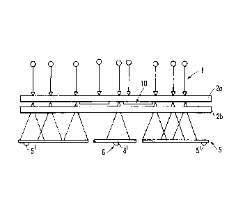
Fig. 8 shows a preferred embodiment of the present
invention and at least in the preferred implementation does not
substantially suffer from the problems associated with
conventional ion detectors or the other arrangements
contemplated and described above. According to the preferred
embodiment an ion detector assembly is provided comprising at
least two microchannel plates 2a,2b and preferably at least a
first collection anode 5 and a second collection anode 6. The
first and second collection anodes 5,6 are preferably co-planar,
but this is not essential.
According to the preferred embodiment a mask 10 is
preferably situated or otherwise positioned between the first
and second microchannel plates 2a,2b. The mask 10 may be
attached to the rear surface of the first microchannel plate 2a
or to the front surface of the second microchannel plate 2b.
According to a particularly preferred embodiment the mask is
sandwiched between the first microchannel plate 2a and the
second microchannel plate 2b.
The shape, size and position of the mask 10 is preferably
such as to align it with the boundaries between the first and
second collection anodes 5,6. Any electron cloud which would
otherwise emerge from the first microchannel plate 2a as a
result of an ion arrival and which would otherwise result in an
electron cloud being emitted from the second microchannel plate
2b which would be shared between the first and second collection
CA 02562747 2006-10-12
WO 2005/104178 PCT/GB2005/001585
- 21 -
anodes 5,6 is preferably substantially prevented from reaching
the second microchannel plate 2b by the mask 10. In this way
the problem of shared electrons between the two collection
anodes 5,6 is preferably substantially eliminated or at least
significantly reduced.
The preferred embodiment as shown in Fig. 8 also
preferably substantially solves the problem of electron clouds
being emitted from the second microchannel plate 2b which can
vary significantly in intensity. Fig. 9 shows an enlarged
portion of the ion detector according to the preferred
embodiment as illustrated in Fig. 8. The mask 10 is shown
positioned so as to prevent an electron cloud due to an ion
arriving at the ion detector being shared between two collection
anodes. The mask 10 also advantageously does not give rise to a
situation wherein only a reduced fraction of secondary electrons
reach a particular collection anode which could otherwise result
in an ion arrival event being missed.
Advantageously, according to the preferred embodiment the
mask 10 also does not stand proud of the input surface of the
first microchannel 2a of the ion detector. Accordingly, the
mask 10 is not exposed to ion bombardment and all the
undesirable consequences associated therewith as discussed above
with reference to the arrangement shown in Fig. 7.
According to the preferred embodiment the thickness of the
mask 10 is preferably as small as possible to avoid unnecessary
spreading in the diameter of the electron cloud incident upon
the input surface of the second microchannel plate 2b. The mask
10 may, for example, have a thickness less than or equal to 25
gm. For a mask thickness of 25 pm the inter-plate gap is
preferably not significantly increased.
The ion detector according to the preferred embodiment is
preferably applicable to systems using a combination of ADC and
TDC detectors with one or more collection anodes.
An embodiment of the present invention is contemplated
wherein the ion detector consists of a stack of more than two
microchannel plates. It is also contemplated that the
microchannel plates 2a,2b may be of equal size or may
alternatively be of unequal size. In the case where more than
CA 02562747 2012-07-20
- 22 -
two microchannel plates are provided the preferred position for
the mask 10 is preferably between the initial two microchannel
plates.
According to an embodiment the larger collection anode 5
may have a circular hole provided in it in which a smaller
circular collection anode 6 may protrude or otherwise be
provided. Alternatively, a rectangular slot may be provided in
the larger collection anode 5 through which a smaller
rectangular collection anode 6 may protrude or otherwise be
provided. Various alternative embodiments are also contemplated
including embodiments wherein the smaller collection anode 6 is
not in the same plane as the larger collection anode 5.
According to further embodiments multiple smaller
collection anodes may be employed. The multiple smaller
collection anodes may be of equal area and/or shape.
Alternatively, the multiple smaller collection anodes may have
unequal areas and/or shapes.