Note: Descriptions are shown in the official language in which they were submitted.
CA 02563154 2006-10-13
WO 2005/106916 PCT/US2005/012438
INTENSIFIED HYBRID SOLID-STATE SENSOR
RELATED APPLICATION
The present application is a continuation-'in-part of pending U.S. Patent
Application No. 09/973,907 filed on behalf of inventors Rudolph G. Benz,
Nils I. Thomas, and Arlynn W. Smith on October 9, 2001, titled INTENSIFIED
HYBRID SOLID-
STATE SENSOR WITH AN INSULATING LAYER, assigned to the assignee of the present
application, and incorporated in this application by reference.
FIELD OF THE INVENTION
The present invention is directed to an intensified hybrid solid-state sensor.
More
1o particularly, the present invention relates to an image intensifier using a
CMOS or CCD sensing
device connected in close physical proximity to a microchannel plate (MCP) and
photo cathode.
BACKGROUND OF THE INVENTION
The present invention relates to the field of image intensifying devices using
solid-state sensors, such as a CMOS or CCD device. Image intensifier devices
are used to
is amplify low intensity light or convert non-visible light into readily
viewable images. Image
intensifier devices are particularly useful for providing images from infrared
light and have many
industrial and military applications. For example, image intensifier tubes are
used for enhancing
the night vision of aviators, for photographing astronomical bodies and for
providing night vision
to sufferers of retinitis pigmentosa (night blindness).
2o There are three types of known image intensifying devices in prior art;
image
intensifier tubes for cameras, all solid-state CMOS and CCD sensors, and
hybrid EBCCD/CMOS
(Electronic Bombarded CCD or CMOS sensor).
Image intensifier tubes are well known and used throughout many industries.
Referring to FIG. 1, a current state of the prior art Generation III (GEN III)
image intensifier
2s tube 10 is shown. Examples of the use of such a GEN III image intensifier
tube in the prior art
are exemplified in U.S. Pat. No. 5,029,963 to Naselli, et al., entitled
REPLACEMENT DEVICE FOR
A DRIVER'S VIEWER and U.S. Pat. No. 5,084,780 to Phillips, entitled TELESCOPIC
SIGHT FOR
DAYLIGHT VIEWING. The GEN III image intensifier tube 10 shown, and in both
cited references,
is of the type currently manufactured by ITT Corporation, the assignee herein.
In the intensifier
3o tube 10 shown in Fig. 1, infrared energy impinges upon a photo cathode 12.
The photo
cathode 12 is comprised of a glass faceplate 14 coated on one side with an
antireflection
layer 16, a gallium aluminum arsenide (GaAIAs) window layer 17 and a gallium
arsenide (GaAs)
active layer 18. Infrared energy is absorbed in GaAs active layer 18 thereby
resulting in the
generation of electron/hole pairs. The produced electrons are then emitted
into the vacuum
3s housing 22 through a negative electron affinity (NEA) coating 20 present on
the GaAs active
layer 18.
CA 02563154 2006-10-13
WO 2005/106916 PCT/US2005/012438
_2_
A microchannel plate (MCP) 24 is positioned within the vacuum housing 22,
adjacent the NEA coating 20 of the photo cathode 12. Conventionally, the MCP
24 is made of
glass having a conductive input surface 26 and a conductive output surface 28.
Once electrons
exit the photo cathode 12, the electrons are accelerated toward the input
surface 26 of the
s MCP 24 by a difference in potential between the input surface 26 and the
photo cathode 12 of
approximately 300 to 900 volts. As the electrons bombard the input surface 26
of the MCP 24,
secondary electrons are generated within the MCP 24. The MCP 24 may generate
several
hundred electrons for each electron entering the input surface 26. The MCP 24
is subjected to a
difference in potential between the input surface 26 and the output surface
28, which is typically
1o about 1100 volts, whereby the potential difference enables electron
multiplication.
As the multiplied electrons exit the MCP 24, the electrons are accelerated
through the vacuum housing 22 toward the phosphor screen 30 by the difference
in potential
between the phosphor screen 30 and the output surface 28 of approximately 4200
volts. As the
' electrons impinge upon the phosphor screen 30, many photons are produced per
electron. The
Is photons create the output image for the image intensifier tube 10 on the
output surface 28 of the
optical inverter element 31.
Image intensifiers such as those illustrated in Fig. 1 have advantages over
other
forms of image intensifiers. First, intensifiers have a logarithmic gain
curve. That is, the gain
decreases as the input light level is increased. This matches the human eye
response
2o particularly when bright lights are in the same scene as low lights. Most
solid-state devices have
a linear response; 1.e., the brighter the light the brighter the output
signal. The result is that
bright lights appear much brighter to a viewer of a solid-state system and
tend to wash out the
scene. Solid-state sensors can be modified to produce a gain decrease as input
light is
increased, however, this requires changing the amplifier gain, using
shuttering, or using
2s anti-blooming control.
Another advantage of image intensifiers is the ability to function over a
large
range of input light levels. The power supply can control the cathode voltage
and thereby
change the tube gain to fit the scene. Thus tubes can function from overcast
starlight to daytime
conditions.
3o However, image intensifier/IZ cameras suffer from numerous disadvantages.
The
electron optics of the phosphor screen produces a low contrast image. This
results in the object
looking fuzzier to the human observer, or solid-state sensor, when viewed
through an image
intensifier. Although this deficiency has been somewhat reduced with further
image intensifier
development, solid-state imagers generally have better performance.
3s Another disadvantage with image intensifier/Iz cameras is ~~halo." Halo
results
from electrons being reflected off either the MCP or the screen. The reflected
electrons are then
amplified and converted into light in the form of a ring around the original
image. In image
CA 02563154 2006-10-13
WO 2005/106916 PCT/US2005/012438
-3-
tubes, the halo from electrons reflected from the MCP has been reduced to a
negligible effect for
the most recent production tubes. However, the halo from the screen section
still exists,
although not to the degree of the cathode halo. Nevertheless, the screen halo
is still a significant
defect in imaging systems when a CCD or CMOS array is coupled to the image
intensifier. This is
s because these arrays are more sensitive than the eye to the low light levels
in the screen halo.
Another disadvantage is that image intensifiers do not have a method of
providing electronic read-out. Electronic read-out is desired so that imagery
from thermal
sensors may be combined with intensified imagery with the result that the
information from both
spectra will be viewed at the same time. One solution has been to create an Ia
camera by
to coupling a CCD or CMOS array to an image intensifier tube. When a solid-
state device is coupled
to an image tube the resultant camera has all performance defects of the image
tube that is low
contrast, often poor limiting resolution due to coupling inefficiencies and
the added cost of the
image tube to the camera.
Solid-state devices typically include CCD or CMOS. They function by directly
is detecting the light, electronically transferring the signal to solid-state
amplifiers, then displaying
the image on either a television type tube or display such as a liquid crystal
display. Figs. 2a and
2b illustrate a flow chart and schematic diagram for a typical CCD sensor.
CCD and CMOS sensors are solid-state devices; that is, there is no vacuum
envelope and the output is an electronic signal that must be displayed
elsewhere and not within
2o the sensor. The solid-state devices operate with power of 5-15 volts. The
light is detected in
individual pixels as labeled °s" and translated into electrons that are
stored in the pixel until the
pixel is read out to the storage register. From the storage register the
electronic information
contained in multiple pixels is then transferred to a read out register and
then to output
amplifiers and then to a video display device such as a cathode ray tube.
2s The disadvantages of an all solid-state device are poor low light level
performance, potential blooming from bright light sources, poor limiting
resolution, and high
power consumption. The poor low light performance is due to dark current and
read-out noise
resulting in low signal-noise ratios. If a signal gain mechanism were provided
prior to read-out
this issue would be negated, as sufficient signal would exist to overcome the
noise sources.
3o Solid-state device architectures usually do not permit an amplification
section prior to read-out.
The poor limiting resolution is due to large pixel sizes usually chosen in an
attempt to collect a
large signal and thereby increase the signal to noise ratio. These
disadvantages have effectively
prevented the use of solid-state sensors in night vision applications. The
advantages of
solid-state devices are better image contrast as compared to the image
intensifier/IZ camera, the
s5 availability of electronic read-out, and lower cost, particularly when the
solid-state sensor is a
CMOS array.
CA 02563154 2006-10-13
WO 2005/106916 PCT/US2005/012438
_q._
As can be seen, the strengths and weaknesses of image intensifiers and
solid-state sensors compliment each other and theoretically a combination of
both devices would
give better performance. One such combination proposed as an alternative to
image
intensifiers/IZ cameras and solid-state sensors, is the electron bombarded
CCD/CMOS sensor
s (EBCCD/CMOS), This device consists of the photo-cathode and body envelope of
the image tube,
and either a CCD or CMOS sensor integrated into this envelope, An illustrative
example of an
EBCCD/CMOS sensor is shown in FIG. 3. A high voltage is applied between the
cathode and
solid-state sensor so that the resulting electrons are amplified within the
silicon in the solid-state
sensor by electron bombardment.
to The advantages of the EBCCD/CMOS device are that it provides electronic
read-out. But the disadvantages are numerous. First, the intra-scene dynamic
range is
compressed. This means that overall contrast within the scene, when bright
objects are next to
dark objects, is reduced compared to an image intensifier/IZ camera and all
solid-state device.
Secondly, the sensor suffers "halo" degradation of the image around bright
lights due to
is electrons reflected off of the solid-state sensor. This halo exists in
regular image tubes;
however, technological improvements have reduced the halo to the point of non-
existence.
Thirdly, the very high voltage required to operate the device (2-10 kV)
damages the silicon
surface causing decay in performance over time.
Therefore, it is an object of the present invention to provide an intensified
hybrid
2o solid-state sensor that combines the functions of the image intensifier,
good signal-to-noise ratio
and high logarithmic gain, with the electronic read-out functions either of a
Complementary
Metal Oxide Semiconductor (CMOS) or Charged Coupled Device (CCD).
SUMMARY OF THE INVENTION
According to an exemplary embodiment of the present invention, an intensified
z5 solid-state imaging sensor includes a photo cathode for converting light
from an image into
electrons. The intensified solid-state imaging sensor also includes an
electron multiplying device
for receiving electrons from the photo cathode. The electron multiplying
device outputs a
greater number of electrons than the electron multiplying device receives from
the photo
cathode. The intensified solid-state imaging sensor also includes a solid-
state image sensor
3o including a plurality of pixels for receiving the electrons from the
electron multiplying device
through a plurality of channels of the electron multiplying device. The solid-
state image sensor
generates an intensified image signal from the electrons received from the
electron multiplying
device. The plurality of channels are arranged in a plurality of channel
patterns, and the plurality
of pixels are arranged in a plurality of pixel patterns. Each of the plurality
of channel patterns is
3s mapped to a respective one of the plurality of pixel patterns such that
electron signals from each
of the plurality of channel patterns is substantially received by the single
respective one of the
plurality of pixel patterns.
CA 02563154 2006-10-13
WO 2005/106916 PCT/US2005/012438
-5-
BRIEF DESCRIPTION OF THE DRAWINGS
In order that the invention will become more clearly understood it will be
disclosed in greater detail with reference to the accompanying drawings, in
which:
Fig. 1 is a schematic illustration of a typical image intensifying tube;
s Fig. 2A is a flow chart for a typical CCD sensor;
Fig. 2B is a schematic diagram of a typical CCD imaging surface;
Fig. 3 is a cross-sectional view of a typical Electron Bombarded CCD device;
Fig. 4A is a cross-sectional view of an intensified hybrid solid-state sensor
according to the present invention;
to Fig. 4B is a schematic representation of an intensified hybrid solid-state
sensor
according to the present invention;
Fig. 5A is a schematic illustration of a microchannel plate (MCP) and a back
thinned CCD for use in the present invention;
Fig. 5B is a schematic illustration of a microchannel plate (MCP) and a
standard
1s CCD for use in the present invention;
Fig. 5C is a perspective view of a CMOS-type image sensor for use with the
present invention;
Fig. 6A is a perspective view of MCP channels having round profiles and a CMOS
well;
2o Fig. 6B is a perspective view of MCP channels having square profiles and a
CMOS
well;
Fig. 7A is a schematic top view of a large pixel/small MCP channel pitch per
unit
area of the sensor surface according to the present invention;
Fig. 7B is a schematic top view of a one-to-one pixel to MCP channel per unit
2s area of the sensor surface according to the present invention;
Fig. 7C is a schematic top view of a small CMOS pixel pitch/large MCP channel
per unit area of the sensor surface according to the invention;
Fig. 8 is an illustration of misalignment of an electron multiplying device
channel
pattern with an image sensor pixel pattern for use in describing the benefits
of exemplary
3o embodiments of the present invention;
Fig. 9A is a block diagram illustration of an aligned electron multiplying
device
channel pattern with an image sensor pixel pattern according to an exemplary
embodiment of
the present invention;
Fig. 9B is a block diagram illustration of another aligned electron
multiplying
3s device channel pattern with an image sensor pixel pattern according to
another exemplary
embodiment of the present invention;
CA 02563154 2006-10-13
WO 2005/106916 PCT/US2005/012438
-6-
Fig. 9C is a block diagram illustration of yet another aligned electron
multiplying
device channel pattern with an image sensor pixel pattern according to another
exemplary
embodiment of the present invention;
Fig. 9D is a block diagram illustration of yet another aligned electron
multiplying
s device channel pattern with an image sensor pixel pattern according to
another exemplary
embodiment of the present invention; and
Fig. 9E is a block diagram illustration of yet another aligned electron
multiplying
device channel pattern with an image sensor pixel pattern according to another
exemplary
embodiment of the present invention.
1o DETAILED DESCRIPTION OF THE INVENTION
Preferred features of embodiments of this invention will now be described with
reference to the figures. It will be appreciated that the spirit and scope of
the invention is not
limited to the embodiments selected for illustration. Also, it should be noted
that the drawings
are not rendered to any particular scale or proportion. It is contemplated
that any of the
is configurations and materials described hereafter can be modified within the
scope of this
invention.
In copending U.S. Patent Application serial number 09/973,907, the present
invention was described as providing an intensified hybrid solid-state sensor.
The solid-state
sensor, according to the present invention, includes an imaging device
comprising a solid-state
2o sensor assembled with an image intensifier cathode, microchannel plate
(MCP), and body
envelope. This device combines the best functions of the image intensifier,
good signal-to-noise
ratio and high logarithmic gain, with the electronic read-out functions either
of a Complementary
Metal Oxide Semiconductor (CMOS) or Charged Coupled Device (CCD), Applications
for this
invention are primarily night vision systems where good low light sensitivity
and high gain are
2s required.
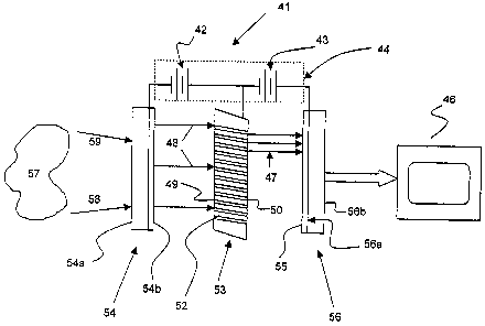
Fig. 4B is a schematic representation of an intensified hybrid solid-state
sensor
device 41 according to the present invention. Sensor 41 comprises a standard
image tube photo
cathode 54, a microchannel plate (MCP) 53 and a solid-state imaging sensor 56.
Solid-state
imaging sensor 56 can be any type of solid-state imaging sensor. Preferably,
solid-state imaging
3o sensor 56 is a CCD device. More preferably, solid-state imaging sensor 56
is a CMOS imaging
sensor. Fig. 5A illustrates a back-thinned CCD imaging device as imaging
sensor 56'. In this
embodiment, MCP 53 is connected with a back-thinned CCD sensor 56'. Back-
thinned CCD 56'
includes an electron receiving surface, such as diffusion collection area 56a'
and a readout
area 62. Fig. 5B illustrates an alternative standard CCD imaging device
including MCP 53
3s connected to a standard CCD 56". CCD 56" includes an oxide cover 63 and
plurality of collection
wells 64. Fig. 5C illustrates the sensor as a CMOS sensor, including a CMOS
substrate 56" and a
plurality of collection wells 65.
CA 02563154 2006-10-13
WO 2005/106916 PCT/US2005/012438
For various reasons, CCD based image sensors are limited or impractical for
use
in many applications. First, CCDs require at least two polysilicon layers with
a buried-channel
implant to achieve their high performance, meaning that they cannot be
fabricated using
standard CMOS fabrication processes. Second, the level of integration that can
be achieved with
s CCD based imagers is low since they cannot include the devices necessary to
integrate them with
other devices in an application. Finally, the circuits used to transfer data
out of the image array
to other devices on the system board, such as Digital Signal Processors (DSPs)
and other image
processing circuits, have a large capacitance and require voltages higher than
the other circuits.
Since the currents associated with charging and discharging these capacitors
are usually
io significant, a CCD imager is not particularly well suited for portable or
battery operated
applications.
As such, less expensive image sensors fabricated out of integrated circuits
using
standard CMOS processes are desirable. Essentially, with a CMOS type imager
sensor, a photo
diode, phototransistor or other similar device is employed as a light-
detecting element. The
15 output of the light-detecting element is an analog signal whose magnitude
is approximately
proportional to the amount of light received by the element. CMOS imagers are
preferred in
some applications since they use less power, have lower fabrication costs and
offer higher
system integration compared to imagers made with CCD processes. Moreover, CMOS
imagers
have the added advantages that they can be manufactured using processes
similar to those
zo commonly used to manufacture logic transistors. While the preferred
embodiment of the
invention incorporates a CMOS sensor as the imaging sensor 56, any solid-state
imaging sensor
would work and is within the scope of the present application.
Referring again to Fig. 4B, photo cathode 54 can be a standard photo cathode
as
used in any known type of image intensifying device. Photo cathode 54 can be,
but is not limited
zs to, a material such a GaAs, Bialkali, InGaAs, and the like. Photo cathode
54 includes an input
side 54a and an output side 54b. MCP 53 can be, but is not limited to a
silicon or glass material,
and is preferably about 10 to 25 mm thick. MCP 53 has a plurality of channels
52 formed
between an input surface 49 and output surface 50. Channels 52 can have any
type of profile,
for example a round profile 52' (Fig. 6A) or a square profile 52" (Fig. 6B.)
MCP 53 is connected
3o to electron receiving surface 56a of imaging sensor 56.
Preferably, output surface 50 of MCP 53 is physically in contact with electron
receiving surface 56a of imaging sensor 56. However, insulation may be
necessary between
MCP 53 and imaging sensor 56. Accordingly, a thin insulating spacer 55 may be
inserted
between output surface 50 of MCP 53 and electron receiving surface 56a of
imaging sensor 56.
3s Insulating space 55 can be made of any electrical insulating material and
is preferably formed as
a thin layer, no more than several microns thick, deposited over electron
receiving surFace 56a of
imaging sensor 56. For example, such an insulating spacer may be, but is not
limited to, an
CA 02563154 2006-10-13
WO 2005/106916 PCT/US2005/012438
_g_
approximately 10 pm thick film. Alternatively, insulating spacer 55 could be a
film formed on the
output surface 50 of MCP 53 (not shown).
CMOS imaging sensor 56 includes electron receiving surface 56a and output 56b.
The increased number of electrons 47 emitted from MCP 53 strike electron
receiving surface 56a.
Electron receiving surface 56a comprises a CMOS substrate 56"' and a plurality
of collection
wells 65 (Fig. 5C). Electrons 47 (See Fig. 4B) collected in collection wells
65 are processed using
standard signal processing equipment for CMOS sensors to produce an
intensified image signal
that is sent through output 56b to an image display device 46.
An electric biasing circuit 44 provides a biasing current to sensor 41.
Electric
1o biasing circuit 44 includes a first electrical connection 42 and a second
electrical connection 43.
First electrical connection 42 provides a biasing voltage between photo
cathode 54 and MCP 53.
The biasing voltage from first electrical connection 42 is preferably set so
as to be less than the
biasing voltage than the EBCCD/CMOS sensor cathode to CCD voltage, i.e., 2-10
kV. For
example, one preferred biasing voltage could be similar to that of image
tubes, such as N1400V.
Second electrical connection 43 applies a biasing voltage of between MCP 53
and CMOS
sensor 56. Preferably, the biasing voltage applied through second electrical
connection 43 is
significantly less than the image tube - screen voltage of about 4200V of the
prior art devices
(Fig. 1). For example, the biasing voltage applied through second electrical
connection 43 could
be, but is not limited to N100V. Fig. 4A illustrates one potential
configuration of the sensor 41.
2o In this configuration, photo cathode 54, MCP 53, and imaging sensor 56 are
maintained in a
vacuum body or envelope 61 as a single unit, in close physical proximity to
each other.
Referring to Fig. 4B, in operation, light 58, 59 from an image 57 enters
intensified hybrid solid-state sensor 41 through input side 54a of photo
cathode 54. Photo
cathode 54 changes the entering light into electrons 48, which are output from
output side 54b
2s of photo cathode 54. Electrons 48 exiting photo cathode 54 enter channels
52 through input
surface 49 of MCP 53. After electrons 48 bombard input surface 49 of MCP 53,
secondary
electrons are generated within the plurality of channels 52 of MCP 53. MCP 53
may generate
several hundred electrons in each of channels 52 for each electron entering
through input
surface 49. Thus, the number of electrons 47 exiting channels 52 is
significantly greater than the
3o number of electrons 48 that entered channels 52. The intensified number of
electrons 47 exit
channels 52 through output side 50 of MCP 53, and strike electron receiving
surface 56a of CMOS
imaging device 56.
Figs. 6A-6B illustrate how the increased number of electrons 47 exit channels
52
(i.e., channels 52' in Fig. 6A, channels 52" in Fig. 6B) and strike a
particular collection well 65' of
3s CMOS imaging sensor 56. As can be seen from these illustrations, a
relationship exists between
the collection wells 65' and the number of channels 52 which emit electrons
47. In general,
CA 02563154 2006-10-13
WO 2005/106916 PCT/US2005/012438
_g_
adjacent channels 52 of MCP 53 are separated by a predetermined channel pitch
52a. Figs. 6A-
6B illustrate a channel pitch 52a that results in more than one channel 52 per
collection well 65'.
Figures 7A-7C illustrate three different alternatives of CMOS well/channel
pitch
relationships according to the invention. Fig. 7A illustrates one relationship
between channel
s pitch 52 and a CMOS well 65'. In this case, channel pitch 52 is relatively
small, while the size of
CMOS well 65' is relatively large. This permits several electrons 47 from two
or more
channels 52 to strike CMOS collection well 65'. Fig. 7B illustrates another
CMOS well/channel
pitch relationship. In this embodiment, channel pitch 52 and the size of CMOS
collection well 65'
are approximately in a one-to-one relationship. As such electrons 47' from a
single channel 52
io strike a single collection well 65'. Fig. 7C illustrates another CMOS
well/channel pitch
relationship where channel pitch 52 is relatively large and the size of CMOS
collection well 65' is
relatively small. In this case electrons 47" from a single channel 52 strike
multiple collection
wells 65'. While each of these structures provide various advantages, the
relationship illustrated
in Fig. 7A is preferred for the present invention.
is As a result, the intensified hybrid solid-state sensor operates in
different
conditions than any of the other prior art concepts. The result is that the
MCP 53 can be
mounted directly on the CMOS sensor 56 giving the hybrid device similar
contrast to the all
solid-state device, but with low halo, good signal-to-noise ratio, and
logarithmic gain of the
image tube. Since operating voltages are lower, the hybrid device can be gated
like an image
2o intensifier allowing operation from overcast starlight condition to daytime
operation. The hybrid
sensor has better halo from the lack of physical gap between MCP 53 and CMOS
sensor 56. This
lack of physical separation in the two components is also why contrast is
improved when
compared to the EBCCD/CMOS or image intensified camera. The hybrid device also
has the
logarithmic gain curve of the image tube. Unlike the EBCCD/CMOS sensor, the
hybrid sensor can
2s be gated due to the low cathode voltages.
Many of the components in image intensifier tubes relate to sampling devices.
Such sampling devices collect a discrete spatial sample of an input signal and
provide a discrete
sampled output signal. Examples of such sampling devices in image intensifier
tubes are the
microchannel plate and the fiber-optic screen. For example, an MCP collects
input electrons in
3o the pores/channels, and outputs electrons from those very same
pores/channels. In the case of
a fiber-optic device, each individual fiber collects a spatial sample of
light, thereby constraining
the light within a fiber, and projecting the sampled image at the output of
the fiber.
When such spatially sampled signals are overlayed on each other several
patterns can be observed at the output. Figure 8 illustrates a configuration
800 relating to pixels
3s of a solid-state image sensor overlayed with channels of an electron
multiplying device. More
specifically, configuration 800 illustrates pixels 802a, 802b, 802c, and 802d
of a solid-state
image sensor overlayed with channels 804a, 804b, 804c, 804d, 804e, 804f, and
8048 of an
CA 02563154 2006-10-13
WO 2005/106916 PCT/US2005/012438
-10-
electron multiplying device. Configuration 800 illustrates misalignment of the
sampling between
the solid-state image sensor and the electron multiplying device. More
specifically, some
portions of channels 804a, 804b, 804c, 804d, 804e, 804f, and 804g align with
pixels 802a, 802b,
802c, and 802d; however, other portions of channels 804a, 804b, 804c, 804d,
804e, 804f, and
8048 do not align with pixels 802a, 802b, 802c, and 802d.
These misalignments, when viewed (e.g., by a person viewing a monitor), can
show up as one of a number of undesirable electro-optical patterns. For
example, such an
electro-optical pattern is known as Moire. Moire (and other electro-optical
patterns such as
aliasing) tend to be very distracting to a person trying to view real objects
through such
to misaligned patterns.
Such optical patterns (i.e., misalignment patterns) often manifest themselves
when the optical transfer quality from one element to another is very good.
For example, Figure
8 illustrates such a high transfer quality. In Figure 8, if the edges of the
pixels and/or channels
were not quite so clear (i.e., the edges were fuzzy), the actual image being
viewed may not
is display the Moire patterns. When the electron multiplying device (e.g., the
MCP) is laid in
contact (or substantial contact) with the solid-state image sensor (e.g., a
CMOS imagery, very
high quality image transfer occurs between the channels of the electron
multiplying device and
the pixels of the solid state image sensor. In such configurations, optical
misalignment patterns
such as Moire would tend to be visible.
2o According to an exemplary embodiment of the present invention, Moire and
other
undesirable optical patterns are avoided or substantially reduced by (1)
arranging a plurality of
channels of an electron multiplying device in a plurality of channel patterns,
(2) arranging a
plurality of pixels of a solid-state image sensor in a plurality of pixel
patterns, and (3) mapping
each of the plurality of channel patterns to a respective one of the plurality
of pixel patterns such
2s that electron signals from each of the plurality of channel patterns is
substantially received by
the single respective one of the plurality of pixel patterns. This alignment
may be in any of a
number of configurations, so long as the signals from each of the channel
patterns is
substantially aligned with the respective one of the pixel patterns such that
optical misalignment
(such as that illustrated in Figure 8) does not occur.
so According to another exemplary embodiment of the present invention, each of
the plurality of channel patterns may be rotationally and translationally
aligned with the
respective one of the plurality of pixel patterns.
For example, Fig. 9A illustrates an exemplary mapping 900, where mapping 900
includes pixels of a solid-state image sensor (arranged as 4 pixel patterns,
each of the pixel
ss patterns including a single pixel) overlayed with channels of an electron
multiplying device
(arranged as 4 channel patterns, each of the channel patterns including a
single channel)
(because of the mapping/registration of the channel patterns to pixel patterns
in Fig. 9A, each of
CA 02563154 2006-10-13
WO 2005/106916 PCT/US2005/012438
-11-
the mappings appears as a single square; however, each of the squares actually
represents a
pixel pattern overlayed with a channel pattern). More specifically, mapping
900 illustrates pixels
902a, 902b, 902c, and 902d (each of which represents a pixel pattern having a
single pixel) of a
solid-state image sensor overlayed with channels 904a, 904b, 904c, and 904d
(each of which
s represents a channel pattern having a single channel). In this embodiment a
single one of
channels 904a, 904b, 904c, and 904d is aligned/mapped with a corresponding one
of pixels
902a, 902b, 902c, and 902d. Further, the channels (e.g., pores of an MCP) are
substantially the
same size as, and have substantially the same center-to-center spacing as, the
pixels (e.g.,
pixels of an image sensor).
io In certain exemplary embodiments of the present invention, it is desirable
to
align the channels of the electron multiplying device with the pixels of the
solid-state image
sensor during assembly of the imaging sensor. One assembly method to ensure
proper
alignment is to shine a light through the electron multiplying device, thereby
allowing for
observation of the reflected pattern of the solid-state image sensor. If no
undesirable
is misalignment pattern is visible (e.g., Moire), then the channels of the
electron multiplying device
are substantially aligned with the pixels of the solid-state image sensor. Of
course, other
methods of alignment are available.
Figure 9A is only one of a number of mapping configurations that provides for
alignment of the channel patterns of the electron multiplying device with the
respective pixel
2o patterns of the solid-state image sensor. A number of additional
configurations are possible.
Figures 9B-9E are additional examples of such mapping configurations.
Figure 9B illustrates an exemplary mapping 910, where mapping 910 includes
pixels of a solid-state image sensor (arranged as 4 pixel patterns, each of
the pixel patterns
including a single pixel) overlayed with channels of an electron multiplying
device (arranged as 4
2s channel patterns, each of the channel patterns including a single channel).
More specifically,
mapping 910 illustrates pixels 912a, 912b, 912c, and 912d of a solid-state
image sensor (each of
which represents a pixel pattern having a single pixel) overlayed with channel
patterns 914a,
914b, 914c, and 914d (each of which represents a channel pattern having a
single channel). In
this embodiment a single one of channels 914a, 914b, 914c, and 914d is aligned
with a
3o corresponding one of pixels 912a, 912b, 912c, and 912d. The embodiment
illustrated in Figure
9B is similar to the embodiment illustrated in Figure 9A in that there is a
one-to-one correlation
between channels of the electron multiplying device and the pixels of the
solid-state image
sensor; however, the channels of the electron multiplying device in Figure 9B
are not
substantially the same size and/or shape as the pixels of the solid-state
image sensor.
ss Regardless, the channels of the electron multiplying device and the pixels
of the solid-state
image sensor are aligned with one another. Because of the alignment, there is
a substantial
reduction in the potential for undesirable optical patterns (e.g., Moire).
CA 02563154 2006-10-13
WO 2005/106916 PCT/US2005/012438
-12-
Figure 9C illustrates an exemplary mapping 920, where mapping 920 includes
pixels of a solid-state image sensor (arranged as 4 pixel patterns, each of
the pixel patterns
including a single pixel) overlayed with channels of an electron multiplying
device (arranged as 4
channel patterns, each of the channel patterns including four channels). More
specifically,
s mapping 920 illustrates pixels 922a, 922b, 922c, and 922d of a solid-state
image sensor (each of
which represents a pixel pattern having a single pixel) overlayed with
channels 924a, 924b,
924c, and 924d (four of which represent a single channel pattern). In this
embodiment a single
one of pixels 922a, 922b, 922c, and 922d is mapped/aligned with a
corresponding channel
pattern, where each of the channel patterns includes four channels (i.e., four
of channels 924a,
924b, 924c, and 924d, respectively). The mapping/alignment of the channel
patterns of the
electron multiplying device and the pixel patterns of the solid-state image
sensor results in a
substantial reduction in the potential for undesirable optical patterns (e.g.,
Moire).
Figure 9D illustrates an exemplary mapping 930, where mapping 930 includes
pixels of a solid-state image sensor (arranged as 9 pixel patterns, each of
the pixel patterns
is including a single pixel) overlayed with channels of an electron
multiplying device (arranged as 9
channel patterns, each of the channel patterns including a single channel).
More specifically,
mapping 930 illustrates pixels 932a, 932b, 932c, 932d, 932e, 932f, 932g, 932h,
and 932i of a
solid-state image sensor (each of which represents a pixel pattern including a
single pixel)
overlayed with channels 934a, 934b, 934c, 934d, 934e, 934f, 934g, 934h, and
934i (each of
2o which represents a channel pattern having a single channel). In this
embodiment a single one of
channels 934a, 934b, 934c, 934d, 934e, 934f, 934g, 934h, and 934i is
mapped/aligned with a
corresponding one of pixels 932a, 932b, 932c, 932d, 932e, 932f, 9328, 932h,
and 932i. The
mapping/alignment of the channel patterns of the electron multiplying device
and the pixel
patterns of the solid-state image sensor results in a substantial reduction in
the potential for
2s undesirable optical patterns (e.g., Moire).
Figure 9E illustrates an exemplary mapping 940, where mapping 940 includes
pixels of a solid-state image sensor (arranged as 4 pixel patterns, each of
the pixel patterns
including four pixels) overlayed with channels of an electron multiplying
device (arranged as 4
channel patterns, each of the channel patterns including a single channel).
More specifically,
3o mapping 940 illustrates pixels 942a, 942b, 942c, and 942d (four of which
represent a single pixel
pattern) of a solid-state image sensor overlayed with channels 944a, 944b,
944c, and 944d of an
electron multiplying device (each of which represents a channel pattern having
a single channel).
In this embodiment a single one of channels 944a, 944b, 944c, and 944d is
mapped/aligned with
a corresponding pixel pattern, where each of the pixel patterns includes four
pixels (i.e., four of
3s wells 942a, 942b, 942c, and 942d, respectively). The mapping/alignment of
the channel
patterns of the electron multiplying device and the pixel patterns of the
solid-state image sensor
results in a substantial reduction in the potential for undesirable optical
patterns (e.g., Moire).
CA 02563154 2006-10-13
WO 2005/106916 PCT/US2005/012438
-13-
The embodiments of the present invention illustrated in Figs. 9A-9E, and
described above, are exemplary in nature. Various alternative configurations
are contemplated.
For example, the number of channels in each of the channel patterns, and/or
the number of
pixels in each of the pixel patterns may be varied in accordance with the
present invention.
s Further, the size and/or shape of the channels and/or pixels may be varied
in accordance with
the present invention. Further still, the mapping of channel patterns to pixel
patterns may also
be varied in accordance with the present invention.
As used herein, a pixel is intended to refer to an element of an image sensor
(e.g., a solid-state image sensor) that receives electrons or electron energy.
Pixels include wells
io for storing the electron energy received.
The above detailed description of a preferred embodiment of the invention sets
forth the best mode contemplated by the inventor for carrying out the
invention at the time of
filing this application and is provided by way of example and not as a
limitation. Accordingly,
various modifications and variations obvious to a person of ordinary skill in
the art to which it
is pertains are deemed to lie within the scope and spirit of the invention as
set forth in the following
claims.