Note: Descriptions are shown in the official language in which they were submitted.
CA 02563182 2006-10-11
DN 52476
MICRO-OPTICAL DEVICE
The present invention relates generally to micro-optical devices. More
particularly, the present invention relates to micro-optical devices that may
be used as
pigtailing assemblies which include a pigtailing chip having an optoelectronic
component and an optical fiber that optically coupled with an optical
component, for
example, one or more waveguides on an integrated optic chip.
Integrated optic chips (IOCs), also referred to as waveguide chips or planar
lightwave circuits, are often pigtailed (or attached) to optical fibers. U.S.
Patent No.
6,839,492, to Kwon et al, discloses such a structure. Often this pigtailing is
done using a
glass, ceramic, or silicon ferrule, containing one or more fibers either
singularly or in a
precision array. The edge of the waveguide and the fiber pigtailing assembly
are butt-
coupled, aligned, and bonded together allowing the light to pass with limited
loss
between the optical fibers and the integrated optic chip. However, a challenge
in
building waveguide devices has been to achieve high performance and low cost
while
additionally incorporating active devices such as lasers and photodetectors.
Historically
active devices are either packaged separately and joined to the waveguide with
an
optical fiber that runs between the devices, or the active devices are placed
directly onto
the integrated optic chip. To couple between the active device and the
waveguides on
the chip, various methods, including the use of grating couplers and embedded
microreflectors in the integrated optic chip have been used. These features
are made to
move the optical light to an elevation out of the plane of the optical
waveguides by
reflecting, refracting, or diffracting the light. Incorporation of such
features into the
waveguide die is usually expensive and requires additional processing steps.
Therefore,
there is a need in the art for technology that provides optical assemblies
that permit high-
performance, low-cost coupling of active optical devices with optical
components such
as waveguides and optical fibers.
The present invention provides a micro-optical device. The micro-optical
device
includes: a first chip which includes a substrate, an optoelectronic component
on the
-1-
CA 02563182 2006-10-11
DN 52476
substrate oriented to optically communicate across a first region of an edge
of the
substrate, and an optical fiber on the substrate oriented to optically
communicate across
a second region of the substrate edge; and an optical component oriented to
optically
communicate with the optoelectronic component and the optical fiber across the
first and
second edge regions, respectively. The optical component is disposed proximate
to the
first chip in an optical path between the optoelectronic component and the
optical fiber.
In one configuration, the optical component is an optical waveguide. The micro-
optical
device may include a second chip, for example, an integrated optic chip, which
includes
the optical component.
The foregoing summary and the following detailed description of the present
invention will be best understood when read in conjunction with the appended
drawings,
in which:
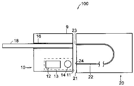
FIG. 1 schematically illustrates a micro-optical device in accordance with the
present invention including a pigtailing chip having an optoelectronic
component and an
optical fiber disposed thereon and including an integrated optic chip butt-
coupled to the
pigtailing chip to permit optical communication between the optoelectronic
component
and the optical fiber;
FIG. 2 schematically illustrates a micro-optical device in accordance with the
present invention including a pigtailing chip having an optoelectronic
component and
2o first and second optical fibers disposed thereon and including an
integrated optic chip
butt-coupled to the pigtailing chip to permit optical communication between
the
optoelectronic component and the first optical fiber and to permit optical
communication
between the first fiber and the second fiber;
FIG. 3 schematically illustrates a micro-optical device in accordance with the
present invention including a pigtailing chip having an optoelectronic
component and
first, second, and third optical fibers disposed thereon and including an
integrated optic
chip butt-coupled to the pigtailing chip to permit optical communication
between the
-2-
CA 02563182 2006-10-11
DN 52476
optoelectronic component and the second optical fiber and to permit optical
communication between the first fiber and the third fiber;
FIG. 4A schematically illustrates a micro-optical device in accordance with
the
present invention including a pigtailing chip having an optoelectronic
component,
optical fiber, and a reflector facet disposed thereon and including an
integrated optic
chip butt-coupled to the pigtailing chip to permit optical communication
between the
optoelectronic component and the optical fiber and to permit optical
communication
between the optical fiber and the reflector facet; and
FIG. 4B schematically illustrates the micro-optical device of FIG. 4A, having
a
1o surface emitting device disposed over the reflector facet in optical
communication with
the reflector facet.
Referring now to the figures, wherein like elements are numbered alike
throughout, a micro-optical device, generally designated 100, in accordance
with the
present invention is provided. The pigtailing assembly 100 includes a
pigtailing
subassembly, such as pigtailing chip 10, which includes a substrate 9, an
active device,
such as an optoelectronic component 12, and includes an optical channel, such
as an
optical fiber 18. As used herein, the term "optoelectronic component" includes
active
devices that emit, detect, or otherwise alter an optical beam, including for
example
optical sources, optical detectors, and MEMS devices. The term "optical
component"
2o includes optical elements, such as optical waveguides, optical fibers,
lenses, gratings,
prisms, filters, and so forth. As used herein, the term "a" and "an" are
intended to
encompass one or more. The term "on" is not limited to elements being directly
in
contact with each other, but may also include intervening layers, structures
and space.
The optoelectronic component 12 and optical fiber 18 are typically oriented on
the pigtailing chip 10 so that the optoelectronic component 12 and optical
fiber 18
optically communicate across a first and second region, respectively, of a
single edge of
the substrate 9, such as coupling edge 11. Such a configuration of the
optoelectronic
component 12 and optical fiber 18, where optical communication of these
elements takes
-3-
CA 02563182 2006-10-11
DN 52476
place across a single edge 11, permits the optoelectronic component 12 and
optical fiber
18 to be butt-coupled to an optical component, such as one or more waveguides
on an
integrated optic chip 20, for example, at a single coupling edge 11 of the
pigtailing chip
10. The integrated optic chip 20 includes a waveguide 22 configured to permit
optical
communication between the optoelectronic component 12 and the optical fiber 18
when
the integrated optic chip 20 is butt-coupled to the pigtailing chip 10.
The integrated optic chip 20 provides one or more functions, indicated by the
broken lines, for example, wavelength multiplexing, wavelength demultiplexing,
optical
attenuation, optical amplification, switching, modulation, and mode
conversion. The
to integrated optic chip may further include one or more additional active
and/or passive
devices (e.g., lasers, photodetectors, integrated circuits, drivers, filters,
lenses, prisms)
thereon or formed therein. High delta-n waveguides such as those based on
silicon
oxynitrides or semiconductors such as silicon, indium phosphide and gallium
arsenide,
or photonic crystal devices, are particularly suitable due to their ability to
be fabricated
with small geometries. Thus, the present invention provides a micro-optical
pigtailing
assembly 100 that permits optical communication between the optoelectronic
component
12 and an optical channel, such as optical fiber 18, via an optical component
such as a
waveguide 22, which may be provided as part of an integrated optic chip. In
one
exemplary application, the micro-optical assemblies of the invention may be
used in a
2o triplexer configuration. Such a configuration finds use, for example, in
fiber-to-the-
home applications, for example, using 1490 nm and 1550 nm incoming and 1310 nm
outgoing signals.
Turning now to FIG. 1 in more detail, the pigtailing chip 10 desirably
contains at
least one active device, such as an optoelectronic component 12, and at least
one optical
channel, such as an optical fiber 18. Optionally, an optical component, such
as a lens
14, may be provided on the pigtailing chip in optical communication with the
optoelectronic component 12 to facilitate the coupling of light to or from the
optical
component 12. (As used herein, the term "light" is not limited to the visible
spectrum,
-4-
CA 02563182 2006-10-11
DN 52476
but includes electromagnetic radiation outside of the visible spectrum.). The
active
device 12 alone or together with other optional components, such as optical
component
14 or other active devices, may optionally be hermetically enclosed so as to
form part of
a hermetically sealed package 13. Such a structure may include, for example, a
transparent wall or lid through which an optoelectronic signal to and/or from
the
optoelectronic component may pass, or a hermetic coating such as a low-
temperature
CVD coating over the optoelectronic component.
The optoelectronic component 12 and optical fiber 18 are desirably provided on
the same substrate 9, so that manufacturing processes, such as
photolithographic
1o processes, may be used to accurately establish the relative position of the
optoelectronic
component 12 to that of the optical fiber 18. For example, the pigtailing chip
may
desirably be single-crystal silicon, which is amenable to photolithographic
processing.
In particular, the location of the optical fiber 18 may be determined by
providing a V-
groove 16 disposed on the upper surface of the pigtailing chip 10. The V-
groove 16 may
be created by etching a single crystal silicon wafer using established or
other suitable
methods. For example, the V-groove 16 may be provided by anisotropic etching
of a
( 100) silicon wafer so that the surfaces of the V-groove 16 are { 111 }
crystallographic
planes. During the same anisotropic etching process, the locations of the
optoelectronic
component 12 and ball lens 14 may be established. For instance, the location
of the ball
lens 14 may be established by providing a pyramidal-shaped pit or V-pit which
may be
etched at the same time as the V-groove 16, whereby the V-pit also includes
surfaces
that are { 111 } crystallographic planes. Likewise, the location of the
optoelectronic
component 12 may be established during the same etching step to provide an
appropriately shaped cavity into which the optoelectronic component 12 may be
seated.
Other suitable chip materials and manufacturing processes may also be used
that permit
precise positioning of the optoelectronic component 12 and optical fiber 18
relative to
one another, along with any other optional components, for example, by
deposition and
-5-
CA 02563182 2006-10-11
DN 52476
etching processes to form alignment fiducials for seating the optoelectronic
and optical
components.
The optoelectronic component 12 (along with optional lens 14) and optical
fiber
18 are oriented on the pigtailing chip 10 so that the optoelectronic component
12 and
optical fiber 18 may communicate across (e.g., over, under, or through) a
single
coupling edge 11 of the pigtailing chip 10, to permit the optoelectronic
component 12
and optical fiber 18 to be optically coupled by butt-coupling to a single
optical
component. For example, the optoelectronic component 12 and optical fiber 18
may be
simultaneously butt-coupled to an integrated optic chip 20. In this regard,
the integrated
optic chip 20 includes an optical waveguide 22 which may include first and
second ends
23, 24 disposed at a coupling surface 21 of the integrated optic chip 20. The
first end 23
and the second end 24 of the waveguide 22 may be optically coupled to the
optical fiber
18 and the optoelectronic component 12, respectively, by placing the coupling
edge 21
of the integrated optic chip 20 in facing opposition to the coupling edge 11
of the
pigtailing chip 10, so that the waveguide and pigtailing chips 20, 10 are butt-
coupled to
one another. To verify that the waveguide ends 23, 24 are properly aligned
with the
optical fiber 18 and the optoelectronic component 12, respectively, to
maximize optical
coupling, the optoelectronic component 12 may be powered or interrogated
during the
process of aligning the pigtailing chip 10 and integrated optic chip 20.
2o For instance, if the optoelectronic component 12 includes a light source,
such as
a laser, the laser may be activated to emit light that is received by the
waveguide 22 and
delivered to the optical fiber 18. A detector may be provided to monitor the
output of
the optical fiber 18 to detect when the chips 10, 20 are best aligned to
maximize the
optical throughput. Alternatively, for example, if the optoelectronic
component 12
includes a detector, a light source may be coupled to the optical fiber 18 at
the end of the
fiber 18 distal to the coupling edge 11, so that the optoelectronic component
12 can
detect when the chips 10, 20 are best aligned to maximize the optical
throughput. Once
the optimal location of the chips 10, 20 is determined, the chips 10, 20 can
be bonded
-6-
CA 02563182 2006-10-11
DN 52476
together allowing the light to pass with limited loss between the optical
fiber 18,
optoelectronic component 12, and waveguide 22. In some cases, however, it may
be
inconvenient or undesirable to power or interrogate the optoelectronic
component 12
during coupling of the pigtailing chip 10 to the integrated optic chip 20. In
such a case,
it may be desirable to provide an additional optical channel on each of the
pigtailing chip
and the integrated optic chip 20, as illustrated in FIG. 2, to permit passive
alignment
of the pigtailing chip 10 and integrated optic chip 20.
For example, with reference to FIG. 2, another exemplary configuration of a
pigtailing assembly, generally designated 200, in accordance with the present
invention
1o is illustrated. Except where noted, the description above with reference to
FIG. 1 is
applicable to FIG. 2 and to the other exemplified aspects of the invention.
The pigtailing
assembly 200 includes a pigtailing subassembly, such as pigtailing chip 210,
which
includes a substrate 209, an active device, such as optoelectronic component
212 and
optional lens 214, and includes at least two optical channels, such as signal
fiber 218 and
alignment fiber 219. The active device 212 alone or together with other
optional
components, such as optical component 214 or other active devices, may
optionally be
hermetically enclosed so as to form part of a hermetically sealed package 213
such as
described above with reference to FIG. 1. In a similar manner to the
pigtailing chip
configuration of FIG. 1, the optoelectronic component 212, signal fiber 218,
and
2o alignment fiber 219 are desirably oriented on the pigtailing chip 210 so
that the
optoelectronic component 212, signal fiber 218, and alignment fiber 219
optically
communicate across first, second and third regions, respectively, of a single
edge of the
substrate 209, such as coupling edge 211, to permit the optoelectronic
component 212,
signal fiber 218, and alignment fiber 219 to be optically coupled by butt-
coupling to a
single optical component.
Provision of a second optical channel, for example, alignment fiber 219,
permits
alignment between the pigtailing chip 210 and optical component such as
waveguides on
integrated optic chip 220, without powering or interrogating the
optoelectronic
CA 02563182 2006-10-11
DN 52476
component 212. The pigtailing chip 210 may be provided by the manufacturing
processes described above with respect to the pigtailing chip 10 of FIG. 1. In
particular,
the locations of the fiber 218, 219 may be determined by providing V-grooves
231, 232
disposed in the upper surface of the substrate 209, and the location of the
optoelectronic
component 212 may be established at the same step to provide an appropriately
shaped
cavity into which the optoelectronic component 212 may be seated. For typical
applications, such as those which include single-mode 1300-1600 nm
communication
devices, the precision with which the components (e.g., fibers 218, 219 and
optoelectronic device 212) are located relative to one another may be, for
example,
to within several microns or less. The integrated optic chip 220 includes a
waveguide 222
configured to permit optical communication between the signal fiber 218 and
the
optoelectronic component 212 and between the signal fiber 218 and the
alignment fiber
219 when the integrated optic chip 220 is butt-coupled to the pigtailing chip
210. In this
regard the waveguide 222 includes a loopback waveguide 233 to permit optical
communication between the signal fiber 218 and the optoelectronic component
212, and
a tap waveguide 234 to permit optical communication between the signal fiber
218 and
the alignment fiber 219, respectively.
The optoelectronic component 212, signal fiber 218, and aligrllnent fiber 219
may be simultaneously butt-coupled to integrated optic chip 220. The
integrated optic
chip 220 includes an optical waveguide 222 which may desirably include first,
second,
and third ends 223, 224, 225 disposed at a coupling surface 221 of the
integrated optic
chip 220. The first end 223 of the waveguide 222 may be optically coupled to
the signal
fiber 218, the second end 224 to the optoelectronic component 212, and the
third end
225 to the alignment fiber 219 by placing the coupling edge 221 of the
integrated optic
chip 220 in facing opposition to the coupling edge 211 of the pigtailing chip
210, so that
the waveguide and pigtailing chips 220, 210 are butt-coupled to one another.
To verify
that the waveguide ends 223, 224 are properly aligned with the signal fiber
218 and the
optoelectronic component 212 to maximize optical coupling, the optoelectronic
_g_
CA 02563182 2006-10-11
DN 52476
component 212 need not be powered or interrogated during the process of
aligning the
pigtailing chip 210 and integrated optic chip 220. Instead, proper alignment
may be
verified by monitoring optical communication between the signal fiber 218 and
alignment fiber 219.
For instance, a light source may be coupled to either the alignment fiber 219
or
the signal fiber 218 at a respective end of the fiber 218, 219 distal to the
coupling edge
211. In addition, a detector may be provided at the distal end of the other
fiber 218, 219
to which the light source is not coupled so that the detector can detect when
the chips
210, 220 are best aligned to maximize the optical throughput. Once the optimal
location
of the chips 210, 220 is determined, the chips 210, 220 can be bonded together
allowing
the light to pass with limited loss between the signal fiber 218,
optoelectronic
component 212, and waveguide 222. Thus, by providing an external light source
and an
external detector, the optoelectronic component 212 need not be powered or
interrogated
during the alignment process.
Still further, another exemplary configuration of a pigtailing assembly in
accordance with the present invention, that may be aligned without the need to
power or
monitor an optoelectronic component 312 is illustrated in FIG. 3 and generally
designated 300. The pigtailing assembly 300 includes a pigtailing subassembly,
such as
pigtailing chip 310, which includes a substrate 309, an active device, such as
an
optoelectronic component 312 and an optional lens 314, and includes at least
three
optical channels, such as a signal fiber 318 and first and second alignment
fibers 317,
319. The active device 312 alone or together with other optional components,
such as
optical component 314 or other active devices, may optionally be hermetically
enclosed
so as to form part of a hermetically sealed package 313 such as described
above with
reference to FIG. 1. In a similar manner to the pigtailing chip configuration
of FIG. 2,
the optoelectronic component 312, signal fiber 318, and alignment fibers 317,
319 are
desirably oriented on the pigtailing chip 310 so that the optoelectronic
component 312,
signal fiber 318, and alignment fibers 317, 319 optically communicate across
first,
-9-
CA 02563182 2006-10-11
DN 52476
second, third and fourth regions, respectively, of a single edge of the
substrate 309, such
as coupling edge 311. In particular, the locations of the signal fiber 318 and
alignment
fibers 317, 319 may be determined by providing V-grooves 331, 332, 333
disposed in
the upper surface of the pigtailing chip 310, and the location of the
optoelectronic
component 312 may be established at the same step by providing an
appropriately
shaped cavity into which the optoelectronic component 312 may be seated.
Provision of second and third optical channels, for example, alignment fibers
317, 319, permits alignment between the pigtailing chip 310 and optical
component such
as one or more waveguides on an integrated optic chip 320 to be accomplished
via
to dedicated alignment channels, for example, alignment fibers 317, 319. Like
the
pigtailing chip 210 of the configuration of FIG. 2, the pigtailing chip 310
may be
provided by similar manufacturing processes having similar precision with
which the
components are located relative to one another.
The integrated optic chip 320 includes a signal loopback waveguide 322
configured to permit optical communication between the signal fiber 318 and
the
optoelectronic component 312, and includes an alignment loopback waveguide 323
configured to permit optical communication between the first alignment fiber
317 and
the second alignment fiber 319 when the integrated optic chip 320 is butt-
coupled to the
pigtailing chip 310. The optoelectronic component 312, signal fiber 318, and
alignment
2o fibers 317, 319 are oriented on the pigtailing chip 310 so that the signal
fiber 318
optically communicates with the optoelectronic component 312 and the alignment
fibers
317, 319 communicate with one another across a single coupling edge 311 of the
pigtailing chip 310, to permit the optoelectronic component 312, signal fiber
318, and
alignment fibers 317, 319 to be optically coupled by butt-coupling to an
optical
component.
The optoelectronic component 312, signal fiber 318, and alignment fibers 317,
319 may be simultaneously butt-coupled to integrated optic chip 320. In this
regard, the
signal loopback waveguide 322 which may desirably include first and second
ends 324,
-10-
CA 02563182 2006-10-11
DN 52476
325 disposed at a coupling surface 321 of the integrated optic chip 320. The
first end
324 of the signal loopback waveguide 322 may be optically coupled to the
signal fiber
318, and the second end 325 to the optoelectronic component 312. Similarly,
the
alignment loopback waveguide 323 may desirably include first and second ends
326,
327 disposed at the coupling surface 321 of the integrated optic chip 320. The
first end
326 of the alignment loopback waveguide 322 may be optically coupled to the
first
alignment fiber 317, and the second end 327 to the second alignment fiber 319.
Thus,
the first and second alignment fibers 317, 319, as well as the signal fiber
318 and
optoelectronic component 312, may be brought into respective optical
communication
by placing the coupling edge 321 of the integrated optic chip 320 in facing
opposition to
the coupling edge 311 of the pigtailing chip 310, so that the waveguide and
pigtailing
chips 320, 310 are butt-coupled to one another.
As with the configuration of FIG. 2, the optoelectronic component 312 need not
be powered or interrogated during the process of aligning the pigtailing chip
310 and
integrated optic chip 320. Instead, proper alignment may be verified by
monitoring
optical communication between the alignment fibers 317, 319. For instance, a
light
source may be coupled to either of the first and second alignment fibers 317,
319 at an
end of the alignment fiber 317, 319 distal to the coupling edge 311. In
addition, a
detector may be provided at the distal end of the other alignment fiber 317,
319 to which
2o the light source was not coupled so that the detector can detect when the
chips 310, 320
are best aligned to maximize the optical throughput. Once the optimal location
of the
chips 310, 320 is determined, the chips 310, 320 can be bonded together
allowing the
light to pass with limited loss between the signal fiber 318 and
optoelectronic
component 312. Thus, by providing an external light source and an external
detector, the
optoelectronic component 312 need not be powered or interrogated during the
alignment
process.
In yet a further exemplary configuration of a pigtailing assembly in
accordance
with the present invention, generally designated 400, a pigtailing assembly is
illustrated
-11-
CA 02563182 2006-10-11
DN 52476
in Figs. 4A and 4B which is particularly suited for pigtailing a surface
emitting (or
receiving) device 450, such as a vertical cavity surface emitting laser
(VCSEL) or
photodetector, for example. The pigtailing assembly 400 includes a pigtailing
subassembly, such as pigtailing chip 410, which includes a substrate 409, an
active
device, such as an optoelectronic component 412 and an optional lens 414, and
includes
an optical channel, such as an optical fiber 418. Optionally, the pigtailing
chip 410 may
include a surface emitting device 450 with or without the optoelectronic
component 412.
Either or both of the active devices 412, 450 together with other optional
components,
such as optical component 414 and other active devices, may optionally be
hermetically
to enclosed so as to form part of a hermetically sealed package 413 such as
described
above with reference to FIG. 1. The location of the optical fiber 418 may be
determined
by providing a V-groove 416 disposed in the upper surface of the substrate
409. In
addition, the pigtailing chip 410 includes a reflector facet 445, which may
desirably be
provided in the pigtailing chip is a { 111 } crystallographic plane in ( 100)
silicon.
The surface emitting device 450 may be desirably disposed over the reflector
facet 445 so that the surface emitting device 450 optically communicates with
the
reflector facet 445, as illustrated in FIG. 4B. The reflector facet 445 is
oriented relative
to a coupling edge 411 of the pigtailing chip 410 so that the surface emitting
device 450
optically communicates across the coupling edge 411 of the pigtailing chip
410. Thus,
2o the optoelectronic component 412, surface emitting device 450, and optical
fiber 418 are
desirably oriented on the pigtailing chip 410 so that the optoelectronic
component 412,
surface emitting device 450, and optical fiber 418 optically communicate
across a single
edge of the substrate 409, such as coupling edge 41 l, to permit the
optoelectronic
component 412, surface emitting device 450, and optical fiber 418 to be
optically
coupled by butt-coupling to an optical component. The pigtailing chip 410 may
be
provided by the manufacturing processes described above with respect to the
pigtailing
chip 10 of FIG. 1. For example, the reflector facet 445 may be provided as a
surface of
a partial V-pit 447. The V-pit 447 with reflector facet 445 may be
manufactured by
-12-
CA 02563182 2006-10-11
DN 52476
anisotropic etching of a (100) silicon wafer during the same step in which the
V-groove
416 is provided. For typical applications, such as those which include single-
mode
1300-1600 nm communication devices, the precision with which the components
(e.g.,
fiber 418, surface emitting device 450, and optoelectronic device 412) are
located
relative to one another may be, for example, within several microns or less.
The integrated optic chip 420 includes a waveguide 422 configured to permit
optical communication between the optical fiber 418 and each of the
optoelectronic
component 412 and the surface emitting device 450 when the integrated optic
chip 420
is butt-coupled to the pigtailing chip 410. In this regard the waveguide 422
includes a
loopback waveguide 433 to permit optical communication between the optical
fiber 418
and the optoelectronic component 412, and a tap waveguide 434 to permit
optical
communication between the optical fiber 418 and the surface emitting device
450.
For example, the optoelectronic component 412, optical fiber 418, and surface
emitting device 450 may be simultaneously butt-coupled to integrated optic
chip 420.
The optical waveguide 422 may desirably include first, second, and third ends
423, 424,
425 disposed at a coupling surface 421 of the integrated optic chip 420. The
first end
423 of the waveguide 422 may be optically coupled to the optical fiber 418,
the second
end 424 to the optoelectronic component 412, and the third end 425 to the
surface
emitting device 450 by placing the coupling edge 421 of the integrated optic
chip 420 in
facing opposition to the coupling edge 411 of the pigtailing chip 410, so that
the
waveguide and pigtailing chips 420, 410 are butt-coupled to one another.
To verify that the waveguide ends 423, 424, 425 are properly aligned with the
optical fiber 418, optoelectronic component 412, and surface emitting device
450,
respectively, either the optoelectronic component 412 or the surface emitting
device 450
may be powered or interrogated during the process of aligning the pigtailing
chip 410
and integrated optic chip 420 in a similar manner as that described above with
reference
to the configuration of FIG. 1.
-13-
CA 02563182 2006-10-11
DN 52476
These and other advantages of the present invention will be apparent to those
skilled in the art from the foregoing specification. For example, multiple
optoelectronic
components may be provided on a single pigtailing chip, along with optional
waveguide
structures on an integrated optic chip for optical communication with each
optoelectronic component. Accordingly, it will be recognized by those skilled
in the art
that changes or modifications may be made to the above-described embodiments
without
departing from the broad inventive concepts of the invention. It should
therefore be
understood that this invention is not limited to the particular embodiments
described
herein, but is intended to include all changes and modifications that are
within the scope
1o and spirit of the invention as set forth in the claims.
-14-