Note: Descriptions are shown in the official language in which they were submitted.
CA 02563281 2006-10-05
1
D E S C R I P T I O N
CARD AND HOST DEVICE
Technical Field
The present invention relates to a card and a host
device, and relates, for example to checking of
operating voltage and capacity of the memory card and
host device.
Background Art
In recent years, a memory card, which is one type
of removable storage device, has been heavily used in
various portable electronic devices such as personal
computers, PDAs, cameras, and mobile phones. PC cards
and small-size SD (trademark) cards draw much attention
as memory cards. The SD (trademark) card is a memory
card which has a flash memory, a card controller and
the like built-in, and is designed in particular to
meet the demands of increased compactness, larger
capacities and higher speeds.
Conventionally, an operating voltage of a memory
card and its host device has been 3.3 V (high voltage)
range and has supported a voltage range from 2.7 V to
3.6 V. Demand has arisen for operation with a lower
voltage, for example, in 1.8 V (low voltage) range, in
other words, which supports a voltage range of 1.65 V
to 1.95 V, for example.
CA 02563281 2010-04-06
2
In addition, the capacity of a conventional memory
card is not sufficient for storing large volumes of
data, and a SD (trademark) card which store large
volumes of data is desired.
Disclosure of Invention
In accordance with one aspect of the invention,
there is provided a host device configured to read and
write information from and into a card and to supply a
supply voltage that belongs to a first voltage range or
a second voltage range which is lower than the first
voltage range. The host device is configured to issue to
the card a voltage identification command including a
voltage range identification section, an error detection
section, and a check pattern section. The voltage range
identification section includes information indicating
which one of the first voltage range and the second
voltage range the supply voltage belongs to. The error
detection section has a pattern configured to enable the
card which has received the voltage identification
command to confirm validity of the voltage
identification command. The check pattern section has a
preset pattern.
The host device may receive a response to the
voltage identification command. The response may include
a voltage range identification section, and an error
detection section or a check pattern section. The error
detection section may have a pattern configured to
enable the host device which may have received the
response from the card to detect errors in the response.
CA 02563281 2010-04-06
3
The host device may issue a next command when the
voltage range identification section of the voltage
identification command and the voltage range
identification section of the response have the same
pattern and the response is confirmed valid using at
least one of the error detection section and the check
pattern.
When the host device receives no response to the
voltage identification command, the host device may
supply a voltage belonging to the first voltage range.
The device may issue an initialization command
including information instructing the card to initialize
a memory that the card may have. The device may change
the definition of the initialization command depending
on whether the device receives a response to the voltage
identification command.
When the host device receives the response of the
voltage identification command, the initialization
command may include information indicating the host
device supports only a small capacity or the host device
supports both a small capacity and a large capacity.
The voltage identification command may include a
first operating voltage identification section or a
second operating voltage identification section. The
first operating voltage identification section may
include a first bit which may correspond to a first
width voltage. The second operating voltage
identification section may include a second bit which
may correspond to a second width voltage which may be
smaller than the first width voltage.
CA 02563281 2010-04-06
3a
In accordance with another aspect of the invention,
there is provided a card. The card includes a memory
which stores information and a controller to control the
memory, the card being operable at only a voltage that
lies within a first voltage range, or at a voltage that
lies within the first voltage range and a voltage that
lies within a second voltage range which is lower than
the first voltage range, and the card being configured
to recognize a voltage identification command including
a voltage range identification section, an error
detection section, and a check pattern section. The card
is operable to issue a response including a voltage
range identification section and an error detection
section or a check pattern section in response to the
voltage identification command. The voltage range
identification section of the response has the same
pattern as the voltage range identification section of
the voltage identification command when the card is
capable of operating in the voltage range specified by
the voltage identification command. The error detection
section of the response has a pattern configured to
enable a device which has received the response to
confirm validity of the response, and the check pattern
section of the response has the same pattern as the
check pattern section of the voltage identification
command.
When the card receives an initialization command
after receiving the voltage identification command and
the card has a small capacity, the card may issue a
response indicating that initialization of the card is
CA 02563281 2010-04-06
3b
completed. When the card receives the initialization
command indicating that a host device supports only a
small capacity and the card has a large capacity, the
initialization of the card may be cancelled.
When the card receives an initialization command
indicating that a host device supports both a small
capacity and a large capacity after receiving the
voltage identification command, the card may issue a
response indicating that initialization is completed
with small capacity when the card has a small capacity
or a response indicating that initialization is
completed with large capacity when the card has a large
capacity.
When the card receives an initialization command
without receiving the voltage identification command and
the card has a small capacity, the card may issue a
response indicating that initialization of the card is
completed. When the card receives the initialization
command without receiving the voltage identification
command and the card has a large capacity, the
initialization may be cancelled.
In accordance with another aspect of the invention,
there is provided a card accessible by a host apparatus.
The card includes a memory which stores information and
a controller for controlling the memory. The card
operates with a supply of a voltage which lies within a
voltage range, and is configured to issue a first
response indicating that an operation voltage of the
card belongs to the voltage range in response with a
reception of a voltage identification command. The card
CA 02563281 2010-04-06
3c
is configured to recognize an initialization command
indicating that the host device supports one of or both
of large capacity or second capacity, and is configured
to issue a second response indicating that the card
supports small capacity or large capacity after
completion of initialization.
The card may abandon initialization when at least
one of no supply of the voltage identification command
and no match between a capacity that the host device
supports and a capacity of the card supports is
satisfied.
Other aspects and features of the present invention
will become apparent to those ordinarily skilled in the
art upon review of the following description of specific
embodiments of the invention in conjunction with the
accompanying figures.
Brief Description of Drawings
Fig. 1 is a diagram schematically showing the main
parts of a card and a host device according to a first
embodiment of the present invention.
Fig. 2 is a diagram showing data arrangement of a
NAND type flash memory in the memory card according to
the first embodiment.
Fig. 3 shows an example of commands issued by the
host device up until immediately before memory
CA 02563281 2006-10-05
4
initialization.
FIG. 4 is a diagram showing the main parts of the
content of a voltage check command.
FIG. 5 is a diagram showing the main parts of the
content of a response to the voltage check command.
FIG. 6 is a flowchart showing a process for
checking an operating voltage range in the case where
the host device operates in a high voltage range.
FIG. 7 is a flowchart of a process for checking an
operating voltage range in the case where the host
device operates in a low voltage range.
FIG. 8 is a diagram showing the main parts of the
content of a memory initialization command according to
a second embodiment of the present invention.
FIG. 9 is a diagram showing the main parts of the
content of a response to the memory initialization
command according to the second embodiment.
FIG. 10 is a flowchart showing a memory
initialization process according to the second
embodiment of the invention.
Best Mode for Carrying Out the Invention
Embodiments of the present invention will be
described in the following with reference to the
accompanying drawings. Note that the structural
elements that have substantially the same function and
configuration in the following description are assigned
the same numbers, and repeated description is provided
CA 02563281 2006-10-05
only when necessary.
(First Embodiment)
A first embodiment relates to reciprocal checking
of an operating voltage range which a host device and a
5 card support.
It is expected that when a card which can operate
in low voltage is realized, a card that supports only
high voltage operation (high voltage card), a card that
supports high voltage and low voltage (dual-voltage
card), and a host device that supplies low voltage and
a host device that supplies high voltage exist in
market.
As a result, when the host device that supplies
low voltage (low voltage host device) and the high
voltage card are used together, the following problems
may arise. When a card is inserted into the host
device, it is initialized by commands from the host
device. At the initialization, the host device issues
to the card commands for acquiring information in a
register that stores information relating to operation
conditions that is provided in the card. The host
device can acquire information on the voltage supported
by the card from the information.
When the information relating to the operation
conditions is acquired, the high voltage card operates
by a low voltage power supply that a host supplies and
outputs information from the operation conditions
CA 02563281 2006-10-05
6
register even though it does not support a low voltage
operation. However, the validity of
transmission/reception of the operation conditions
register information cannot be guaranteed because the
card operates by a voltage which it does not support.
For this reason, the host device attempts
initialization of the inserted card and in the case
where the initialization fails to know that the card
does not support the low voltage operation.
Note that when the conventional host device that
supplies high voltage and the two-voltage card are used
together, there is no particular problem because both
can operate at high voltage.
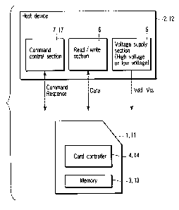
FIG. 1 schematically shows the main parts of the
card and host device according to the first embodiment
of the invention. As shown in FIG. 1, the card 1
includes a memory 3 and a card controller 4.
The card 1 supports only a high voltage operation
(for example, 3.3 V) or supports both high voltage and
low voltage operations (for example, 1.8 V). Note that
low voltage operation refers, in reality, that the card
1 and the host device 2 are configured to support a
voltage range including 1.8 V (such as 1.65 V to
1.95 V). Similarly, the high voltage operation refers
that the card 1 and the host device 2 are configured to
support a voltage range including 3.3 V (such as 2.7 V
to 3.6 V). Typically, the range of the operating
CA 02563281 2006-10-05
7
voltage itself is the same for both the card 1 and the
host device 2. An unused voltage region is provided
between the low voltage range and the high voltage
range.
The host device 2 includes a voltage supply
section 5, a read/write section 6, and a command
control section 7. The voltage supply section 5
operates with a high voltage or low voltage power
source potential Vdd, and the power source potential
Vdd and a common potential Vss are supplied to the
card. The read/write section 6 reads data from the
card 1 and writes data onto the card 1. The command
control section 7 transmits and receives commands and
responses to and from the card 1. Reference numerals
11, 12, 13, 14 and 17 will be explained in a second
embodiment.
A NAND type flash memory may be used as the memory
3. FIG. 2 shows arrangement of data in the NAND type
flash memory. Each page of the NAND type flash memory
11 has 2122 Bytes ((512 Bytes data memory section +
16 Bytes redundant section) x 4), and 128 pages form
one erasure unit (256 kBytes + 8 kBytes).
In addition, the NAND type flash memory 21 has a
page buffer 21A for inputting and outputting data into
and from the flash memory. The memory capacity of the
page buffer 2lA is 2112 Bytes (2048 Bytes + 64 Bytes).
At the time of data writing and the like, the page
CA 02563281 2006-10-05
8
buffer 21A performs processing of inputting and
outputting data into and from the flash memory in 1
page units corresponding to its own capacity.
When the memory capacity of the NAND flash memory
21 is, for example, 1 Gbit, the number of 256-kByte
blocks (erasure units) is 512. In addition, the NAND
flash memory 21 is manufactured by using, for example,
0.09- m process technology. That is, the design rule
of the NAND type flash memory 21 is less than 0.1 m.
Meanwhile, the embodiment shows the case where the
erasure unit is a 256-kByte block, but construction
such that the erasure unit is, for example, a 16-kByte
block is also advantageous in practical use. In this
case, each page has 528 Bytes ((512 Bytes data memory
section + 16 Bytes redundant section), and 32 pages
form one deletion unit (16 kBytes + 0.5 kBytes (k is
1024). In addition, the NAND flash memory 21 may be a
binary memory which stores 1 bit of information in one
memory cell, or may be a multi-value memory which
stores 2 bits or more of information in one memory
cell.
Next, the initialization method using the card 1
and the host device 2 in FIG. 1 will be described with
reference to FIGS. 3 to 7. The initialization process
includes various processings. First, an outline of
commands issued by the host device 2 up until
immediately before memory initialization will be
CA 02563281 2006-10-05
9
described. FIG. 3 shows an example of the commands
issued by the host device 2 up until immediately before
memory initialization. Note that the card 1 and the
memory 2 operates with the operating voltage until
information is acquired from the operation conditions
register of the memory 2 by a memory initialization
command described hereinafter. During this time, the
card 1 must be operable by the operating voltage.
As shown in FIG. 3, when initialization is
started, the host device 2 issues a reset command CMDR
to reset circuits in the card 1.
Next, the host device 2 issues a voltage check
command CMDV. The command is a newly introduced
command in this embodiment. For this reason, the
conventional card 1 does not recognize the voltage
check command CMDV, and even if it receives this
command, it does not send back a response to the host
device 2. The host device 2 and the card 1 can check
the operating voltage (operating voltage range)
supported by each other using the voltage check command
CMDV. The reciprocal checking method will be described
in detail hereinafter.
Next, if the card 1, for example, supports various
I/O functions that are expanded from a data storage
function, the host device 2 issues an initialization
command CMDIO to the card 1. Subsequently, an
initialization command for the memory 1 is supplied.
CA 02563281 2006-10-05
Memory initialization will be described using the
second embodiment.
Now, the voltage check command CMDV will be
described. FIG. 4 shows the main parts of the content
5 of the voltage check command CMDV. As shown in FIG. 4,
the voltage check command CMDV has at least a check
pattern section CPS and a voltage range identification
section VOLS. The voltage range identification section
VOLS has a pattern which uniquely shows whether the
10 host device 2 supports a low voltage operation or a
high voltage operation.
The check pattern section CPS and the voltage
range identification section VOLS can have any number
of bits. However, it is preferable that the following
conditions are satisfied. Namely, as described in the
following, the operation of the host device 2 and the
card 1 examine whether the bit pattern of the voltage
range identification section VOLS match or not to check
the operating voltage range for each other. For this
reason, the check pattern section CPS may be, for
example, about 8 bits and the voltage range
identification section VOLS may be, for example, about
4 bits in order to avoid incorrect recognition when the
pattern for this section changes due to noise. The
command section CM has an index for identifying this
command.
In order to check whether or not the command is
CA 02563281 2006-10-05
11
correctly transmitted from the host device 2 to the
card 1, the voltage check command CMDV has an error
detection code section ED which uses an error detection
code section ED using an error detection code or the
like such as CRC (Cycle Redundancy Check). The card 1
can detect an error inside the voltage check command
CMDV by using the error detection code.
FIG. 5 shows the main parts of the content of a
response to the voltage check command CMDV. As shown
in FIG. 5, the response to the voltage check command
includes at least a check pattern section CPA and a
voltage range identification section VOLA. The card 1
forms the same bit pattern as the voltage check command
CMDV in the check pattern section CPA, and forms the
same bit pattern as the voltage range identification
section VOLS in the voltage range identification
section VOLA to thereby send a response to the host
device. The response may have an error detection code
section ED as in the case of the voltage check command
CMDV. The host device 2 can use the error detection
code or compare the response with the command to
determine if they match in order to detect errors in
the response of the voltage check command CMDV.
Next, description will be given to a method in
which the host device 2 and the card 1 check the
operating voltage range which each other supports by
using the voltage check command CMDV. The process
CA 02563281 2006-10-05
12
differs depending on a high voltage range operation or
a low voltage range operation. First, the process of
the high voltage range operation will be described.
FIG. 6 is a flowchart showing a process for checking
the operating voltage range when the host device 2
operates in the high voltage range. As shown in
FIG. 6, the host device 2 issues the voltage check
command CMDV to the card 1 in step ST1.
In step ST2, the host device 2 determines whether
or not there is a response to the voltage check command
CMDV. As described above, the conventional card does
not recognize the voltage check command CMDV, and thus
does not issue a response to the command. For this
reason, the host device 2 determines that the card 1 is
not a low voltage card, or in other words, it
determines that the process by the high voltage
operation can be continued, and takes the memory
initialization process. The memory initialization
process will be described in the second embodiment.
Meanwhile, when the card 1 under initialization is
the card of this embodiment, the card 1 sends back the
response shown in FIG. 5 to the host device 2. At this
step, the card 1 first observes a bit pattern of the
voltage range identification section VOLS of the
voltage check command CMDV. Then, the card 1 sends
back the response which has the same bit pattern as
this bit pattern in the voltage range identification
CA 02563281 2006-10-05
13
section VOLA.
Next, in step ST3, the host device 2 checks the
matching of the pattern of the voltage range
identification section VOLA in the response and the
pattern of the voltage range identification section
VOLS in the voltage check command CMDV. When these
pattern match, the host device 2 determines that the
card 1 is a new card for which the voltage check
command CMDV can be checked and that the operating
voltage range of the host device 2 is supported.
Simultaneously, the host device 2 executes CRC
check or checks that the bit pattern of the response
matches the bit pattern of the command. Consequently,
it can be confirmed that the transmission and reception
of the voltage check command CMDV are reliable.
In the case of a bus mode with an error detection
code in a command, the pattern of the error detection
code section ED in the response is formed into, for
example, a CRC code to check the validity of the
response. In the case of a bus mode without error
detection code section ED in the voltage check command
CMDV, the voltage range identification section VOLS and
the voltage range identification section VOLA as well
as the check pattern sections CPS and CPA of the
command and response respectively match, and the
response is determined to be normal. If the response
is determined to be normal, the voltage check process
CA 02563281 2006-10-05
14
ends. Then, the flow transfers to the memory
initialization process. This will be described in the
second embodiment.
On the other hand, if the voltage range
identification section VOLS and the voltage range
identification section VOLA do not match and/or the
check pattern section CPS and the check pattern section
CPA do not match, and an error is detected by the error
detection code, the process for checking the operating
voltage range ends. As a result, the initialization
process stops.
FIG. 7 is a flowchart showing a process for
checking the operating voltage range when the operating
voltage of the host device 2 is within the low voltage
range. The difference between the low voltage
operation and the high voltage operation lies only in
the following point. Namely, if there is no response
from the card 1 in step ST2, this means that the card 1
does not operate with low voltage. Thus, the
initialization process stops in order to avoid
initialization on the high voltage card by the host
device 2 that operates in the low voltage range.
According to the card 1 and the host device 2 of
the first embodiment of the invention, the card 1 and
the host device 2 can know the operating voltage range
that each other supports based on
transmission/reception of the newly provided command.
CA 02563281 2006-10-05
For this reason, the subsequent initialization process
can be performed by normal operation using the
operating voltage range that the card 1 and the host
device 2 both support. In addition, when the operating
5 voltage range that both support do not match, the host
device 2 can detect this and cancel the initialization
process. As a result, it is possible to avoid wasteful
process such as initialization in an abnormal state and
a malfunction of the host.
10 In addition, according to the first embodiment,
the voltage check command CMDV has a check pattern, and
the card 1 forms the same pattern as the check pattern
in the response to the voltage check command CMDV.
Comparing the check patterns can provide guarantee of
15 the reliability of transmission and reception of the
voltage check command CMDV. Accordingly, even when the
bus mode without code error detection section in each
command, errors can be detected in the response.
(Second Embodiment)
A second embodiment relates to a method of memory
initialization depending on whether a memory loaded in
a card is of a large capacity or a small capacity.
With the realization of a card capable of storing
large volume of information (large capacity card), it
is necessary to newly set a format corresponding to the
large capacity card. A file system of a new format is
different from that of a conventional low capacity
CA 02563281 2006-10-05
16
format. In addition, a conventional host device which
uses the low capacity format cannot recognize the file
system of the large capacity card. For this reason, if
the conventional host device initializes the large
capacity card, data on the card may be destroyed.
The following four combinations are possible
according to whether or not the host device supports
large capacity and whether or not the card that is
being initialized supports large capacity.
(1) Conventional host device (which does not support
large capacity) + small capacity card
(2) Conventional host device + large capacity card
(3) Large capacity supporting host device (also
supports small capacity) + small capacity card
(4) Large capacity supporting host device + large
capacity card.
It is desirable that the host device and/or the
card detect which of the above cases applies and
responds accordingly.
As shown in FIG. 1, a card 11 according to the
second embodiment of the invention is loaded with a
small capacity or large capacity memory 13 and a card
controller 14. A host device 12 includes a command
control section 17. The command control section 17 is
configured to support a memory initialization command
of the second embodiment described and both the small
capacity card and the large capacity card as well as
CA 02563281 2006-10-05
17
the functions of the command control section 7 of the
first embodiment.
The content of the memory initialization command
differs depending on where the process reaches in the
flowchart of the first embodiment. If the results of
the operating voltage range checking determines that
the process has reached A in FIG. 6, the host device 12
has a function for issuing the voltage check command
CMDV and is thus not a conventional format, or in other
words, it supports large capacity. In addition, the
case in which the card being initialized is a small
capacity card, the case (3) above is applicable. In
this case, the host device 12 issues a conventional
memory initialization command. The card controller 14
of the card 1 receives the conventional memory
initialization command to initialize the memory into a
mode that is compatible with the prior art.
On the other hand, in the case where the process
reaches B in FIG. 6 or FIG. 7, the host device 12
performs memory initialization by using a new
initialization command shown hereinafter. FIG. 8 shows
the main parts of the content of the new memory
initialization command according to the second
embodiment of the invention. As shown in FIG. 8, the
memory initialization command includes a first voltage
identification section V1S, a second voltage
identification section V2S, a capacity identification
CA 02563281 2006-10-05
18
section HCS, and a busy notification section BS. The
second voltage identification section V2S may be
omitted, and only the first voltage identification
section V1S may be defined.
The first voltage identification section V1S is
configured by, for example, multiple bits, and each bit
corresponds to a specific width of voltage (such as
0.1 V). A voltage range supported by the first voltage
identification section V1S is the same as the high
voltage operation range of the first embodiment. A bit
showing the voltage being currently applied at the host
device 12 is set to "1".
The second voltage identification section V2S may
be configured by 1 bit. It may also be formed of a
plurality of bits. The bit is set if the host device
12 applies voltage in the low voltage range. When the
second voltage identification section V2S is configured
by multiple bits, the width of the voltage covered by
each bit in the second voltage identification section
V2S can be less than that for the first voltage
identification section V1S, and may be unit of 0.05 V,
for example. By doing this, even if the operating
voltage of the host device and the card is decreased
even further in the future, the host device can show
its own operating voltage in more detail. A voltage
range supported by the second voltage identification
section V2S is the same as the low voltage range of the
CA 02563281 2006-10-05
19
first embodiment.
A middle voltage range section VM is provided
between the voltage range covered by the first voltage
identification section V1S and the voltage range
covered by the second voltage identification section
V2S. The host device 12 does not support the voltage
range corresponding to the middle voltage range section
VM, and as a consequence, all of the bits in the middle
voltage range section VM never show "1".
The following advantages are obtained by providing
the middle voltage range section VM. The card
controller 14 has a voltage regulator in order that the
card 11 can correspond to two operating voltage ranges.
The voltage regulator determines whether a supply
voltage from the host device 12 is high voltage or low
voltage, and changes the supply voltage to the
operating voltage of the card 11. At this time, if two
operating voltage ranges are successive, the voltage
regulator finds it difficult to determine a voltage
which is substantially in the middle of the two
operating voltage ranges. As a result, the operation
slowly progresses. To avoid that, a region that is not
for use is provided to help the voltage regulator
easily determine the range of the supply voltage.
The capacity identification section HCS has a
pattern which indicates whether the host device 12
supports only small capacity or both small capacity and
CA 02563281 2006-10-05
large capacity. The busy notification section BS is
set to 0 or 1 in the response, and is constant (for
example, 0) in the command. The new memory
initialization command may have an error detection
5 section ED composed of a CRC code and the like.
FIG. 9 shows the main parts of the content of the
response of the memory initialization command according
to the second embodiment. As shown in FIG. 9, each
part of the response of the memory initialization
10 command has the same format as the command, and
includes a first voltage identification section ViA, a
second voltage identification section V2A, a capacity
identification section HCA, and a busy notification
signal BA.
15 The first voltage identification section ViA has
the same number of bits as the first voltage
identification section V1S in the command, and all of
the bits corresponding to the operating voltage that
the card 11 itself supports may be, for example, "1".
20 Similarly, the second voltage identification
section V2A also has the same number of bits as the
second voltage identification section V2S in the
command. All of the bits corresponding to the
operating voltage that the card 11 itself supports may
be, for example, "1".
The capacity identification section HCA indicates
whether the card 11 is a small capacity card or a large
CA 02563281 2006-10-05
21
capacity card. The busy notification section BS forms
a bit pattern during the memory initialization, the bit
pattern indicating this fact.
Next, the method for memory initialization will be
described with reference to FIG. 10. FIG. 10 is a
flowchart showing the memory initialization process
according to the second embodiment of the invention.
FIG. 10 shows the portion following A and B in FIGS. 6
and 7. That at least both the card 11 and the host
device 12 support issuing the voltage check command
CMDV is necessary to issue a new memory initialization
command. In addition, when the card 11 is a large
capacity card, the new memory initialization command
must be issued.
As shown in FIG. 10, in step ST11, the host device
12 issues a new memory initialization command shown in
FIG. 8. If the host device 12 supports a large
capacity card, the capacity identification section HCS
of this command is set to a bit pattern that indicates
that the host device 12 supports a large capacity card.
Note that when the host device is a conventional
type, the voltage check command CMDV and the memory
initialization command (new memory initialization
command) according to this embodiment are not issued.
In addition to it, when the card being initialized is a
small capacity card, which corresponds to (1) above,
the card 11 is initialized (including the operation of
CA 02563281 2006-10-05
22
the card 11 sending back a response) in a mode that is
compatible with the prior art by means of the
conventional initialization command.
When the host device is the conventional type, and
the card 11 that being initialized is a large capacity
card, which corresponds to (2) above, the card 11 which
has not received the voltage check command CMDV does
not complete initialization instructed by the memory
initialization command in order to cancel the
initialization process. The host device, then, detects
that the initialization could not be performed based on
a time limit check. This makes it possible to prevent
initialization of the large capacity card by the small
capacity format in error.
Next, in step ST12, the host device 12 determines
existence of a response to the new memory
initialization command. When no response is received,
it is assumed that an error occurred and the processing
ends. When a response is received, the host device 12
checks in step ST13 the bit pattern of the busy
notification section BA in the response. The host
device 12 keep issuing the memory initialization
command until the initialization of the memory ends and
the bit pattern indicates that memory initialization
has ended (step ST14). Once initialization of the
memory 13 starts, the card only sends back a response
and ignores the content that has been set in the memory
CA 02563281 2006-10-05
23
initialization command parameters. The host device 12
checks the limits for the time for which the memory 13
is being initialized.
When the initialization of the memory 13 is
complete, the host device 12 checks the bit pattern of
the capacity identification section HCA in the response
in step ST15. The capacity identification section HCA
comes in effect when initialization ends. If the card
11 being initialized is a new card and of a small
capacity card, HCA = 0 is shown, which corresponds to
the case (3) above. As a result, the host device 12
knows that the card has been initialized as a small
capacity card. If it is a large capacity card, HCA = 1
is shown, which corresponds to the case (4) above. As
a result, the host device 12 knows that the card has
been initialized as a large capacity card. The
process, then, transfers to an additional process (for
example, acquisition of an ID of the card 11).
In the host device 12 and the card 11 according to
the second embodiment of the invention, the memory
initialization command and response includes support
information and identifying information for the small
capacity card or the large capacity card. The host
device 12 and the card 11 use it to check whether a
host device with which it is in communication supports
large capacity. The high capacity card 11 is
initialized only when both the host device 12 and the
CA 02563281 2006-10-05
24
card 11 support high capacity. The small capacity card
is initialized only when both the host device 12 and
the card 11 support small capacity. Also, because the
host device 12 which supports large capacity must also
support small capacity, the initialization process is
cancelled when the small capacity host attempts to
initialize the large capacity card 11. Consequently,
even when the new or old host devices are used with the
new or old cards, errors in operation can be prevented.
In addition, various modifications and adjustments
within the scope of the present invention may occur to
one skilled in the art, and it is to be understood that
these modifications and adjustments are included in the
scope of the invention.
Industrial Applicability
According to the present invention, a card and a
host device can be provided, in which reciprocal
checking of the operating voltage and capacity is
possible.