Note: Descriptions are shown in the official language in which they were submitted.
CA 02563457 2012-07-23
Inverter Bridge Controller Implementing Short-Circuit Protection Scheme
BACKGROUND OF THE INVENTION
1. Field of the Invention
100011 Fault handling in inverter bridges utilizing Insulated Gate Bipolar
Transistors
(IGBTs) and similar switching devices, such as inverter bridges utilized with
three-phase
AC motors.
2. Description of the Related Art
100021 Inverter bridges provide controlled energy used to drive inductive
loads. A
plurality of switches within the inverter bridge are sequentially switched to
vary the
inverter bridge's output voltage. Typically, output is a three-phase
alternating current
voltage. For a general background description of inverter bridge topologies,
sequential
switching schemes, and circuits and procedures for performing sequential
switching
schemes, PCT Publications WO 02/37654 A2 published 10 May 2002 and WO
2004/015851 A2 published 19 February 2004. An exemplary three- level inverter
bridge
topology is illustrated in FIG. 1.
[0003] In conventional inverter bridges, fault conditions (short-circuits) can
be
characterized as falling into one of two categories. A first category is a
Type I fault.
Typically, a Type I fault is the result of a fault inside the drive (for
example, an IGBT
failure or an output fault with low inductance). As a result of the low
impedance, the
increase in current (di/dt) through the IGBT is high, such that the IGBT is
forced to
desaturate.
- 1 -
CA 02563457 2006-10-13
WO 2006/002229
PCT/US2005/022046
[0004] When a Type I fault is detected, the switches of the inverter bridge
are sequentially
commanded to an off-state. Because the switches are not saturated, the current
decays slowly,
causing no appreciable voltage spikes. Therefore, Type I faults for two-level
inverter bridges are
fairly easy to manage, and numerous methods are known in the art.
[0005] A second category is a Type II fault, which is typically a fault
external to an inverter
bridge, such as a cable short-circuit or motor fault. The impedance in the
circuit undergoing fault
is typically high, resulting in the current through the IGBT rising slowly.
The result is that the
IGBT saturates under the Type H fault condition; or a Type II fault may occur
while a particular
IGBT is already in saturation.
[0006] Under a Type II fault condition, the IGBT can be quickly turned off
when the IGBT is
commanded to an off-state while in saturation. However, such switching while
in saturation
results in a voltage spike that may destroy the transistor. The voltage spike
is due to a counter-
electromotive force produced by the negative current di/dt times a leakage
inductance of the
circuit. Under a Type II fault, the currents rise to levels several times
higher than the rated
nominal current of the IGBT.
[0007] A Type II short-circuit fault is the worst case for an inverter bridge,
particularly in a
multiple-level (three-or-more level) inverter bridge, because it allows the
IGBT to saturate during
a fault condition. Type II faults involve a short-circuit path inductance
which causes a limited
di/dt current increase, which will allow the current to rise well above the
maximum rated current
of the IGBT, but will not allow the IGBT to enter desaturation.
[0008] Existing solutions to this problem generally create other problems. For
example,
adding additional circuitry to an inverter bridge to cut off power to the
inductive load, without
- 2 -
CA 02563457 2006-10-13
WO 2006/002229
PCT/US2005/022046
commanding off the IGBTs, as a practical matter, increases the leakage
inductance of the inverter
bridge circuit, thereby causing otherwise innocuous current switching di/dts
to generate harmful
voltage spikes. In comparison, if the switches are commanded off during a Type
II fault and the
fault current rises above the maximum rated current of the IGBT, then the IGBT
will most likely
be destroyed by the voltage spike generated by the negative current di/dt.
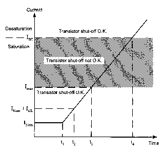
[0009] As shown in FIG. 2, at the initiation (t1) of a Type II fault, current
rises slowly.
However, the time between an inverter controller recognizing an overload
situation (t2) and when
the short circuit current exceeds a maximum rated current (t3) is often less
time than an individual
IGBT requires to switch off. Because of inherent time delays which increase
with the power-
handling capacity of the switch used, the fault current continues to rise,
entering a forbidden
region for switch shut-off before the controller can act, or before a switch
commanded to shut-off
actually does shut-off.
[0010] One way to slow the rise time down further is artificially increase
inductance at the
output of the inverter bridge. However, this increases losses and does not
address the situation
when the inductance itself is the cause of the short-circuit.
[00111 Once the fault current enters the forbidden region for switch shut-of
safe shut off is
only possible if the current thereafter decreases below the maximum rated
current (Imax) of the
IGBT, or when the current exceeds the required current to desaturate the IGBT.
However, once
an IGBT reaches desaturation current levels under a fault condition (t4),
there is very little time to
turn off the switch before there is thermal damage to the IGBT.
[0012] To date, in conventional designs, there is always a fault current
inductance that will
cause any inverter bridge to risk destruction when commanding the IGBTs to an
off-state during a
- 3 -
CA 02563457 2006-10-13
WO 2006/002229
PCT/US2005/022046
Type II fault. Moreover, with conventional inverter bridges, even when the
inverter bridge
controller commands switches off in a proper sequence, since desaturation
ordinarily occurs
randomly among the switches in series, destruction of the switches may
nonetheless occur.
SUMMARY OF THE INVENTION
[0013] The invention is a new control scheme for the protection of Insulated
Gate Bipolar
Transistors (IGBTs) in an inverter bridge in the case of short-circuit,
including type II faults.
Transistors experiencing a Type II fault turn off quickly. The principles of
the invention hold true
for any AC drive -- low, medium or high voltage -- from any manufacturer.
Additionally, the
principles hold true when the inverter bridge switches are other types of
transistors which
experience desaturation under fault conditions, such as bipolar junction
transistors (BJTs) and
field effect transistors (FETs).
[0014] A three-phase inverter bridge has three branches and "L" bus voltage
levels (L > 2).
Each branch provides one phase of the three-phase output for driving an
inductive load. An
exemplary three-level inverter bridge is illustrated in FIG. 1, and single
branches of two-level,
four-level, and five-level inverter bridges are illustrated in FIGS. 3, 4, and
5.
[0015] One of the L levels is a most-negative bus voltage and one of the L
levels is a most-
positive bus voltage. Any intermediate bus voltage levels are differentiated
from other bus
voltage levels by:
V MostPositive ¨VMosiNegatzve
(L ¨1)
- 4 -
CA 02563457 2006-10-13
WO 2006/002229 PC
TIUS2005/022046
[0016] Each branch of an inverter bridge comprises two half-branches: a first
one-half branch
comprising switches connected between the most-positive bus voltage and a
respective phase
output, and a second one-half branch comprising switches connected between the
most-negative
bus voltage and the respective phase output.
[0017] In a half-branch of an inverter bridge having three-or-more levels, the
direction toward
the most-positive rail or most-negative rail is referred to as "outer,"
whereas the direction toward
the phase output is referred to as "inner." For example, referring to FIG. 5,
switches S1 and S8
are the outermost switches, whereas switches Szt and S5 are the innermost
switches.
[0018] When shutting off switches, whether under normal operating conditions
or fault
conditions, it is essential to shut off switches in each half branch
sequentially from outer to inner,
as is known in the art. The present invention facilitates safe shutting off of
outer switches by
increasing the probability that the outer switches desaturate and shut-off
first.
[0019] A first aspect of the invention is a method of controlling an inverter
bridge, which for
each branch comprises comparing an instantaneous output current (I0) of a
phase of the three-
phase output of the inverter bridge with a rated nominal current of a switch
(IN.) of the switches
of the branch plus an overload current threshold (lot.). The overload current
threshold IOLiS
selected so that Ia. + 'Nom satisfies I,.> + 'Nom > 'Nom, 'max being a maximum
rated current of
the switches of the branch. If 1I01 > 'Nom TOL, then the switches that are
conducting the
instantaneous output current (I.) exceeding IN. + are identified, and an off-
state is secured for
switches that are identified as not conducting Ic and being in an off-state.
If switches of the
branch have an on-state in a half-branch that is not conducting the
instantaneous output current
-5.-
CA 02563457 2006-10-13
WO 2006/002229
PCT/US2005/022046
(I0) exceeding 'Nom ToL, the switches in that half-branch are sequentially
turned off in a
conventional manner.
[0020] The instantaneous current (1) is also compared with
If IN.. + < V < all
switches of a half-branch conducting To remaining in an on-state are
sequentially commanded to
assume an off-state, while continuing to compare for IL] > T. Until a time
elapsed after the last
switch is commanded to an off-state exceeds a wait time (toff), the comparison
for ILI >
continues. The wait time (toff) is defined as a rated turn-off time of the
switches, which is a sum
of a turn-off delay time plus current fall-time.
[0021] If ILI > I.., a most outer switch remaining in an on-state is checked
for desaturation.
A way to check for desaturation, if the switches are insulated gate bipolar
transistors (IGBTs) or
bipolar junction transistors (BJTs) is by determining whether a collector-to-
emitter voltage (V..)
of the switch and is above a rated saturation collector-to-emitter voltage
(Vce sat) of the switch,
wherein the switch is not desaturated if V... < Vce sat and is desaturated if
Voo > Vce sat.
[0022] If the switch is not desaturated, the most outer switch remaining in an
on-state is kept
an on-state, and any switches between the most outer switch and the phase
output are kept in an
on-state. If the most outer switch and any switches between the most outer
switch remaining in
an on-state and the phase output have been commanded to an off-state, then
those switches are
commanded back to an on-state. Then a waiting period begins, delaying until a
sooner of
desaturation and expiration of a delay period based upon an amount of time
before the switches
remaining in an on-state are damaged. The delay period can be either be pre-
set or feedback-
based, and preferably corresponds to a time for a temperature of the most
outer switch remaining
in an on-state to reach a maximum rated temperature value.
- 6 -
CA 02563457 2006-10-13
WO 2006/002229
PCT/US2005/022046
[0023] If the most outer transistor switch is desaturated or when the delay
period expires, the
most outer switch remaining in an on-state is turned off, and then if any
switches remain in an on-
state, the process is repeated from comparing the instantaneous output current
(I.) exceeding 'Nam
+ ICI, with Imax.
[0024] If a feedback-based delay period is utilized, and the switches are
insulated gate bipolar
transistors (IGBTs) or bipolar junction transistors (BJTs), determining the
time for the
temperature of the most outer transistor switch remaining in an on-state to
reach the maximum
rated temperature value based on the instantaneous current Io according to:
( Vce=sat x /0 I, dt > ce.max V L ¨1 x / sc
where lice,. is defined as a maximum rated collector-to-emitter voltage of the
most outer
transistor switch remaining in an on-state, and I. is defined as a maximum
rated short circuit
current per transistor switch.
[0025] If a pre-set delay time is utilized, the switches are insulated gate
bipolar transistors
(IGBTs) or bipolar junction transistors (BJTs), determining the time for the
temperature of the
most outer transistor switch remaining in an on-state to reach the maximum
rated temperature
value can be determined to approximately equal:
tsc. x rcsa,
Vcemax
where tse max. is defined as a rated maximum short-circuit time duration which
the transistor switch
can withstand when submitted to Vce. and I.
[0026] The rated nominal current of the transistor switch (INon,), the maximum
rated current of
the transistor switch (I.), the rated saturation collector-to-emitter voltage
(Vce sat), the maximum
- 7 -
CA 02563457 2006-10-13
WO 2006/002229
PCT/US2005/022046
rated temperature value, the maximum rated short circuit current per
transistor switch (1,c), and
the rated maximum short-circuit time duration (t õ,õõx) which the transistor
switch can withstand
when submitted to Vce ma. and Lc, can be ordinarily be determined from a
manufacturer's
specification for the transistor switch.
[0027] As a further variation on the first aspect of the invention, when the
delay period
expires without desaturation, prior to turning off the most outer transistor
having an on-state, the
phase output is shunted to a neutral voltage level (if not already shunted).
The neutral voltage
level is a difference of the most-positive bus voltage and the most-negative
bus voltage, divided
by two.
[0028] As an embodiment of this fiirther variation, when the half branch
conducting I is a
first one-half branch (switches between the most-positive bus voltage and the
phase output), the
shunting of the phase output to the neutral level shunts the first one-half
branches of all three
branches of the three-phase inverter bridge. When the half branch conducting
Io is a second one-
half branch (switches between the most-negative bus voltage and the phase
output), the shunting
the phase output to the neutral level shunts the second one-half branches of
all three branches of
the three-phase inverter bridge.
[0029] As another embodiment, the shunting of the phase output to the neutral
level shunts all
half branches of all three branches of the three-phase inverter bridge.
[0030] A second aspect of the invention is a three-phase inverter controller
controlling a
three-phase inverter bridge. For each branch, the controller comprises at
least a first comparison
circuit, a second comparison circuit, a delay circuit, and logic circuitry.
- 8 -
CA 02563457 2006-10-13
WO 2006/002229
PCT/US2005/022046
[0031] The first comparison circuit compares an instantaneous output current
(L) of a phase
of the three-phase output of the inverter bridge with a rated nominal current
(IN..) of the switches
of the branch plus an overload current threshold (Ju). The overload current
threshold IoL is
selected so that + IN.. satisfies I. > IoL + IN0. > IN.., wherein I. is a
maximum rated current
of the switches of the branch.
[0032] If1101> 'Nom IOL, but if ILI <I, then the logic circuitry identifies
switches of the
branch that are conducting the instantaneous output current (I.) exceeding
IN0. + In, secures an
off-state to switches that are identified as not conducting I and being in an
off-state, and
sequentially, from outer to inner, commands off switches within a half-branch
containing switches
that have an on-state but are not conducting the instantaneous output current
(I.) exceeding 'Nom
+ IoL=
[0033] The second comparison circuit compares the instantaneous output current
(I.) with
While ILI > IN.. + IoL and 1101 I, the logic circuitry sequentially, from
outer-to-inner,
commands all switches remaining in an on-state to assume an off-state.
[0034] While ILI > I, the logic circuitry sequentially checks whether a most
outer switch
remaining in an on-state is desaturated. If not desaturated, then the logic
circuitry keeps the most
outer switch remaining in an on-state and any switches between the most outer
switch and the
phase output in an on-state, and if the most outer switch and any switches
between the most outer
switch remaining in an on-state and the phase output have been commanded to an
off-state, then
these transistor switches are commanded back to an on-state. The logic
circuitry then waits until
a sooner of desaturation and an expiration of a delay period of the delay
circuit. The delay period
- 9 -
CA 02563457 2006-10-13
WO 2006/002229
PC T/US2005/022046
is preferably set based upon an amount of time before the switches remaining
in an on-state are
damaged.
[0035] If most outer switch remaining in an on-state is (or becomes)
desaturated or when said
delay period expires, then the logic circuitry turns off the most outer switch
remaining in an on-
state, after which, a next most outer switch, if any, remaining in an on-state
is checked for
desaturation.
[0036] As an embodiment of the second aspect of the invention, the logic
circuitry checks
whether a most outer switch remaining in an on-state is desaturated by
checking a signal received
from a driver card driving the most outer transistor switch remaining in an on-
state. This
embodiment is convenient when utilizing driver cards that include the
monitoring of saturation as
a feature.
[0037] The delay period of the delay circuit is preferably set so that
expiration of the delay
period corresponds to a time for a temperature of the most outer transistor
switch remaining in an
on-state to reach a maximum rated temperature value.
[0038] As an embodiment of the second variation of the invention, the first
comparison circuit
comprises a first comparator, and the second comparison circuit comprises a
second comparator.
[0039] A third aspect of the invention is a method of protecting switches of a
three-phase
inverter bridge when a short occurs and at least one of the transistor
switches is allowed to
saturate due to a short-circuit inductance. A short-circuit is detected by
comparing output
currents of each phase of the three-phase output of the inverter bridge with a
threshold current
level. In each branch providing one of the three-phase outputs in which a
short-circuit is detected,
a determination is made as to whether each switch of the branch having an on-
state is saturated,
- 10 -
CA 02563457 2006-10-13
WO 2006/002229 PCT/US2005/022046
and if it is determined that at least one transistor switch is saturated, the
phase corresponding to
the branch is shunted to a neutral voltage level. The neutral voltage level is
a difference of the
most-positive bus voltage and the most-negative bus voltage, divided by two.
[0040] As an embodiment of the third aspect of the invention, for each switch
determined to
be saturated, a determination is made as to which one-half branch contains the
respective switch.
When a saturated transistor switch is determined to be in one of the first one-
half branches of the
inverter bridge (switches connected between the most-positive bus voltage and
a respective phase
output), shunting comprises half-wave rectifying the phase output so as to
pass that portion of the
phase output having a more-positive bus voltage level than the neutral voltage
level, and
connecting the half wave rectified phase output to the neutral voltage level.
When a saturated
transistor switch is determined to be in one of the second one-half branches
of the inverter bridge
(switches connected between the most-negative bus voltage and the respective
phase output),
shunting comprises half-wave rectifying the phase output so as to pass that
portion of the phase
output having a more-negative voltage level than the neutral voltage level,
and connecting the
half-wave rectified phase output to the neutral voltage level.
[0041] As another embodiment of the third aspect of the invention, the phase
output is
rectified and shunted so that the portions of the phase output above the
neutral voltage level
(positive) and below the neutral voltage level (negative) are shunted to the
neutral voltage level.
[0042] A fourth aspect of the invention is a "crowbar" protection circuit for
protecting
switches of a three-phase inverter bridge when a short occurs and at least one
of the switches is
allowed to saturate due to a short-circuit inductance. The crowbar circuit
comprises at least one
switch, selectively shunting each phase of the three-phase output of the
inverter bridge to a
-11-
CA 02563457 2006-10-13
WO 2006/002229 PC T/US2005/022046
neutral voltage level. The neutral voltage level is a difference of the most-
positive bus voltage
and the most-negative bus voltage, divided by two. By closing the at least one
switch, thereby
shunting each phase to the neutral voltage, saturated switches of the three-
phase inverter bridge
become desaturated.
[0043] If the inverter bridge has an odd number of levels (L), the neutral
voltage level
corresponds to one of the "L" bus voltage levels of the inverter bridge.
However, if "L" is an
even number, the neutral voltage level is between two of the "L" bus voltage
levels of the inverter
bridge.
[0044] As an embodiment of the fourth aspect of the invention, the crowbar
circuit is
provided within a separate housing from the three-phase inverter bridge,
configured to be
electrically connected to the three-phase output of the inverter bridge.
[0045] As a further embodiment of the fourth aspect of the invention, the at
least one switch
of the crowbar circuit comprises a first switch and a second switch, The
crowbar circuit further
comprises a first set of three diodes, each diode of the first set having an
anode connected to a
respective phase output of the three-phase output of the inverter bridge, the
cathodes of the first
set of three diodes being connected to said first switch. By closing the first
switch, the first switch
selectively shunts a first half-wave rectified portion of the three-phase
output to the neutral
voltage level. The crowbar circuit also includes a second set of three diodes,
each diode of the
second set having a cathode connected to a respective phase output of the
three-phase output of
the inverter bridge, the anodes of the second set of three diodes being
connected to said second
switch. By closing the second switch, the second switch selectively shunts a
second half wave
rectified portion of the three-phase output to the neutral voltage level.
- 12 -
CA 02563457 2006-10-13
WO 2006/002229
PCT/US2005/022046
[0046] The first and second switch can be configured to be closed
collectively, shunting both
half-wave rectified portions to the neutral voltage level, or the first and
second switch can be
configured to be closed individually.
[0047] A fifth aspect of the invention is a storage medium storing a set of
program
instructions for a controller, the controller being configured to control a
three-phase inverter
bridge. The set of program instruction, when executed by the controller, cause
the controller to
control the inverter bridge according to any of the above aspects of the
invention.
[0048] These above aspects of the invention mitigate damage from Type I and
Type II faults.
When saturation occurs, by delaying until a sooner of desaturation of the most
outer transistor
remaining in an on-state and the expiration of the delay period, the
statistical likelihood of switch
survivability is markedly improved. While waiting until the brink of
destruction to turn a switch
off may still result in destruction caused by the -di/dt voltage spike if the
switch is still saturated,
statistical switch survivability is improved in comparison to when a switch
conducting an overload
current is allowed to cross into saturation after being commanded to an off-
state, or is
immediately commanded to an off-state while already in saturation. The closer
the delay period is
set to the time that destruction of the switches will occur, the greater the
probability that
desaturation will occur, in comparison to commanding switches off as soon as
an overload is
detected.
[0049] Further, by shunting the overload current to a neutral level, a lower
impedance path is
offered to the overload current, thereby immediately desaturating the most
outer switch remaining
in an on-state, allowing the inverter bridge to be shut down quickly and
safely.
- 13 -
CA 02563457 2006-10-13
WO 2006/002229
PCT/11S2005/022046
BRIEF DESCRIPTION OF THE DRAWINGS
[0050] FIG. 1 illustrates an exemplary three-level inverter bridge circuit
having an AC motor
as the inductive load.
[0051] FIG. 2 is a current-time graph illustrating a change in current over
time during a Type
II fault.
[0052] FIG. 3 illustrates a single branch of a two-level inverter bridge.
[0053] FIG. 4 illustrates a single branch of a four-level inverter bridge.
[0054] FIG. 5 illustrates a single branch of a five-level inverter bridge.
[0055] FIGS. 6A, 6B, 7A, 7B, 8A, and 8B illustrate a flow diagram of exemplary
embodiments for controlling an inverter bridge.
[0056] FIGS. 9, 10, and 11 are a flow diagram according to another exemplary
embodiment
for controlling an inverter bridge.
[0057] FIG. 12 illustrates an exemplary embodiment of the controller
interfacing with driver
cards and inverter-bridge output transducers according to the present
invention.
[0058] FIG. 13 illustrates a driver card connected to an IGBT.
[0059] FIG. 14 illustrates an inverter bridge modified, according to the
present invention, with
output transducers and a "crowbar" protection circuit.
[0060] FIGS. 15 and 16 are logic diagrams of a controller for controlling an
inverter bridge
using desaturation signals provided by driver cards.
[0061] FIG. 17 is a logic diagram of a controller for controlling an inverter
bridge determining
desaturation based on output current.
- 14 -
CA 02563457 2006-10-13
WO 2006/002229 PC
T/US2005/022046
[0062] FIGS. 18A and 18B demonstrate how to integrate desaturation fault
signals from the
driver cards into the designs of FIGS. 15, 16, and 17.
[0063] FIG. 19 is a logic diagram for determining the polarity of the
instantaneous output
current.
[0064] FIG. 20 is a two-level inverter bridge branch providing a neutral
voltage level for use
with the crowbar protection circuit of the present invention.
[0065] FIG. 21 is a four-level inverter bridge branch providing a neutral
voltage level for use
with the crowbar protection circuit of the present invention.
DETAILED DESCRIPTION OF EXEMPLARY EMBODIMENTS
[0066] In the present disclosure, in the context of switching, the terms "on-
state,"
"conducting," and "closed" are interchangeable, as are the terms "off-state,"
"non-conducting,"
and "open".
[0067] FIGS. 6A, 6B, 7A, 7B, 8A, and 8B are a flow diagram illustrating
exemplary
embodiments for controlling an inverter bridge. The embodiments focus on a
single phase output
of the inverter bridge, representative of what is done for each of the three
phase outputs.
[0068] Referring to FIG. 6A, the instantaneous output current Io of the phase
is compared to
a rated nominal current the rated nominal current (IN0m) of switches of the
branch plus an overload
current threshold (10L) (step 601). INom is the nominal maximum current (100%
current) that a
switch can withstand without regard to temperature (provided the temperature
is inside the rated
range of the switch). In comparison, Imax is a maximum rated current of the
switches of the
branch, which typically is a maximum continuous current a switch can withstand
and be safely
- 15 -
CA 02563457 2006-10-13
WO 2006/002229
PCT/1JS2005/022046
turned-off Typically, Imaõ is 200% of the nominal current, and represents the
threshold above
which turn-off is not allowed when the switch is not desaturated.
[0069] The selection ofloL depends upon considerations such as the fault
sensitivity desired
for a specific application, but Icc IN= should satisfy Im> + 'Nom > 'Nom. By
selecting a large
IoL, the number of nuisance ("false positive") short-circuit detections is
reduced, but the chances
of successfully shutting down before the instantaneous current I. reaches I.
is decreased since
there is less time to respond and shut switches off before entry into the
region in which ILI > Im
in case of a Type II fault. In comparison, by selecting a small IoL, system
sensitivity to short
circuits is increased, and the chances of successfully shutting down before
reaching saturation is
increased. However, the compromise made by increasing sensitivity is nuisance
shut downs
caused by operational fluctuations in the load. A preferred value for ICH, +
IN= is 125% of the
nominal current.
[0070] If I has not exceeded Tim 'Nom in the branch under examination, the
branch is
presumed not to be experiencing a fault or short-circuit. Preferably, a check
is made as to
whether any of the other branches are experiencing a fault (step 602). If
there is a fault in one of
the other branches, the original branch is sequentially shut down in the
conventional fashion (step
604). If the method is implemented as a periodic check in a single-pass
manner, then once the
branch is shut down, or if no faults are detected, the procedure for that
branch is over. In the
alternative, as shown in FIG. 6B, initial fault detection handling for a
branch can be implemented
as a continuous loop, where the branches are continually checked for fault
conditions (loop
formed by steps 601 and 603).
-16-
WO 2006/002229 CA 02563457 2006-10-13
PCT/US2005/022046
[0071] If a fault is detected, (1I0r > -1- Tot), several steps are performed
to shut down
switches that are not in the overload path. The switches in the fault path are
identified (step 610),
any switches that are already off (non-conductive) are secured in the off-
state (step 611), and
switches that have an on-state, but are not conducting Ii,, are sequentially
switched off from outer-
to-inner in the conventional fashion (step 612).
[0072] As shown in FIG. 7A, instantaneous output current 10 is also compared
to Irooõ (step
620). If the instantaneous current Io crossing over IN. Iot, has not exceeded
Imo., the switches
can be shut down sequentially in a conventional manner (step 621). However, as
is the case
during ordinary operation, the switches must be shut off sequentially to avoid
that a switch is
biased at a voltage that exceeds the switch's maximum operating voltage. For
an IGBT or BIT,
this maximum operating voltage is Vcoõõ),. In view of this need for sequential
switching, and since
a switch commanded off does not actually stop conducting until toff (a sum of
a turn-off delay time
of the switch plus the current fall-time) elapsed, the instantaneous output
current must be
continually monitored during the sequential shut down to assure that the
switch current does not
exceed Imax during shut down (step 621). Once the last switch is commanded
off, even though the
Imox current level has not been detected, it is still necessary to monitor
whether the instantaneous
output current 10 exceeds Imoõ until toff has transpired (steps 622, 623), due
to the delay between
commanding a switch off and when the switch actually stops conducting current.
[0073] FIG. 7B is an alternative approach to the procedure shown in FIG. 7A.
Whereas a
conventional sequential switch shut-off procedure may command off an outer
switch in a half-
branch, and then command off the next switch in the half-branch before toff is
reached for the
outer switch, FIG. 7B illustrates a simple procedure which completely shuts
off each switch
-17-
CA 02563457 2006-10-13
CA 02563457 2006-10-13
WO 2006/002229
PCT/1JS2005/022046
before proceeding to the shut off of the next switch. The instantaneous output
current Io is
compared to I (step 625). If I. has not reached the Imoõ level, the most outer
switch having an
on-state is commanded off (step 626). A loop is then entered, waiting for the
switch to shut
completely off (step 627), while continually checking to assure that the I.
does not reach the In.
level (step 628). Once the switch is completely off, if there are any switches
remaining in the half
branch having an on-state (step 629), shut-off continues by repeating the
process on the most
outer switch having an on-state (i.e., next switch inward from the last switch
that was shut off).
[0074] While the half-branch shut-down routine of FIG. 7B is conceptually
simpler than the a
conventional sequential shut-down (step 621 in FIG. 7A), a longer time is
likely required before
the branch is completely shut off. Accordingly, the chances of lo reaching In.
during the shut
down sequence is increased. However, if a two-level inverter is being shut
down, the time to
complete the processes in FIGS. 7A and 7B are substantially identical, since
there is only one
switch to shut off in a half-branch.
[0075] As shown in FIG. 8A, if Io does exceed Imax, while a switch in the path
of Io has
entered into saturation, a different shut down routine is initiated. A most-
outer switch remaining
in an on-state (conducting) is checked for desaturation (step 630). If the
most-outer switch
having an on-state is desaturated, the switch is turned off. Preferably,
turning the switch off
comprises commanding the switch off (step 631), and then checking whether the
switch has shut
off (step 633) and whether the switch is no longer desaturated (step 634). If
the switch becomes
saturated after being commanded off, the switch is commanded back on (step
640). Otherwise,
once the switch is oft a check is made as to whether any switches in the half-
branch remain on
- 18-
CA 02563457 2006-10-13
WO 2006/002229
PC T/US2005/022046
(step 636). If switches remain on, the process is repeated for the next most-
outer switch
remaining on, returning to step 620 (FIG. 7A) or step 625 (FIG. 7B).
[0076] Nailer checking for desaturation (step 630), the most outer switch
remaining in an on-
state is not desaturated, the most outer switch having an on-state is kept on,
or commanded on, as
well as all switches of the half-branch between the most outer switch having
the on-state and the
phase output (step 640). Then a wait begins, lasting until an earlier of an
expiration of a delay
period (step 650) or the desaturation of the most outer switch having the on
state. The delay
period preferably corresponds to a time for a temperature of the most outer
switch remaining in
an on-state to reach a maximum rated temperature value. Preferably, if a pre-
set delay is used and
the switches are BJTs or IGBTs, then as illustrate in Fig. 8A the delay period
approximately
equals:
tsctr x Vce=sal
Võ..
where Vce max is defined as a maximum rated collector-to-emitter voltage of
the switch, I. is
defined as a maximum rated short circuit current per switch, and ts. is
defined as a rated
maximum short-circuit time duration which the switch can withstand when
submitted to V..
and Is, .
[0077] In comparison, if a feedback-based delay is used as shown in Fig. 8B
(step 655), then
the delay period should approximately be:
7 V x/
flu ce-satX1 -10 I) at > c e.max s c
L-1
[0078] An advantage of feedback-based delay is it can be more accurate, since
current level
information is continually acquired and constantly updated.
-19-
CA 02563457 2006-10-13
WO 2006/002229
PCT/US2005/022046
100791 Conceptually, by waiting as long as possible before switching off a
saturated switch,
the probability of desaturation occurring increases, thereby statistically
improving the survivability
of the switch, so long as the switch is not destroyed in the interim. Any
method of determining
such a delay, whether pre-set or feedback-based, may be suitably utilized.
[0080] As a further improvement, if either delay period (steps 650 or 655)
expires, the phase
output is shunted to a neutral voltage level (steps 660, 661). Shunting the
phase output converts
a Type II fault into a Type I fault, which should force the switches to
desaturate. Shunting the
phase output further improves the survivability of the switches of the
inverter bridge.
[0081] FIGS. 9, 10, and 11 are a flow diagram of another exemplary embodiment
for
controlling an inverter bridge, illustrating an implementation of the method
of FIGS. 6A, 7A, and
8B including the use of indexing variables.
[0082] Referring to FIG. 9, the instantaneous output current Ic, of the phase
is compared to a
rated nominal current the rated nominal current (IN.) of switches of the
branch plus an overload
current threshold (10L) (step 901). If I. has not exceeded IoL, + INom in the
branch under
examination, a check is made as to whether any of the other branches are
experiencing a fault
(step 902). If there are not faults, the procedure can either end (as
illustrated) or be repeated
from step 901. If there is a fault in one of the other branches, the original
branch is sequentially
shut down in the conventional fashion (step 904).
100831 If a fault is detected, (III > + Tot), a determination of polarity of
the fault current
is made in order to determine which half branch is conducting I. (step 910).
If the instantaneous
current is positive, the fault lies in the positive-side half-branch, whereas
if the instantaneous
current is negative, the fault lies in the negative-side half-branch.
- 20 -
CA 02563457 2006-10-13
WO 2006/002229 PC T/US2005/022046
[0084] If the fault is in the positive-side half-branch, a variable "i" is set
equal to the number
of levels "L" in the inverter bridge (step 911), and a variable "p" is set
equal to two (step 912).
Referring to the switch numbering pattern used in the present disclosure in
which, for each
branch, switch 1 is the switch closest to the most-negative bus, and switch
2(L-1) is the switch
closest to the most-positive bus, switches (L-1) to 1 are kept off (step 913),
corresponding to the
switches of the half-branch between the most negative bus and the phase
output.
[0085] A determination is made as to whether switch "?' has an on-state (step
914). If switch
"i" is on, Variable "i" is then incremented (step 915) and a check is made to
determine whether
"i" has exceeded the number of switches in the branch (i> 2(L-1)) (step 916).
If "i" has not
exceeded the number of switches in the branch, the loop is repeated from step
914. If "i" has
exceeded the number of switches in the branch (step 916), or if an outer
switch of the positive-
side half-branch is off (step 914), "i" is decremented (step 917). By
decrementing "i" (step 917),
the value of "i" is set to reference the most outer switch of the half branch
remaining in an on-
state.
[0086] In comparison, if the negative-side half-branch is conducting the fault
current, then at
step 921, the value of "i" is set to the reference number of the innermost
switch of the negative-
side half-branch (i = L - 1). A variable "p" is set equal to 1 at step 922.
Switches L to 2(L - 1)
are kept off (step 923), corresponding to the switches of the half-branch
between the most
positive bus and the phase output.
[0087] A determination is made as to whether switch "i" has an on-state (step
924). If switch
"i" is on, Variable "i" is then decremented (step 925) and a check is made to
determine whether
"i" equals zero (step 926). If "i" is not zero, the loop is repeated from step
924. If"?' is zero
-21 -
CA 02563457 2006-10-13
WO 2006/002229 PCT/US2005/022046
(step 926) or if an outer switch of the negative-side half-branch is off
(steps 924), "i" is
incremented (step 927). By incrementing "i" (step 927), the value of "i" is
set to the reference the
most outer switch of the half branch remaining in an on-state.
[0088] Although not shown, if an inner-most switch of a half branch conducting
the
instantaneous current Io is determined to be off (non-conducting), the process
can either end or be
repeated from step 901. However, such an occurrence may indicate a sensor
failure, including a
failure in the circuit monitoring the output current or the circuit monitoring
the innermost switch.
One approach to handling such an occurrence would be to set "i" to indicate
the outermost switch
of the half-branch, and proceed with sequential shut-down.
[0089] As shown FIG. 10, instantaneous output current Io is compared to L.
(step 930). If
the instantaneous current Io crossing over 'Nom 101, has not exceeded I,, the
switches can be
shut down sequentially in a conventional manner (step 931). However, since a
switch
commanded off does not actually stop conducting until toff, the instantaneous
output current must
be continually monitored during the sequential shut down to assure that switch
saturation does
not occur during shut down (step 931). Once the last switch is commanded off,
even though the
Imax current level has not been detected, it is still necessary to monitor
whether the instantaneous
output current I. exceeds I,,,a. until toff has transpired (steps 938, 939),
since there is a delay
between commanding a switch off and when the switch actually stops conducting
current.
[0090] As shown in FIG. 11, if Io does exceed I., a most-outer switch
remaining in an on-
state is checked for desaturation (step 940). If the most-outer switch having
an on-state is
desaturated, the switch is turned off (step 941).
-22 -
CA 02563457 2006-10-13
WO 2006/002229
PCT/US2005/022046
[0091] A check is made as to whether any switches in the half-branch remain
on, and if
switches remain on, the process is repeated for the next most-outer switch
remaining on, returning
to step 930 (FIG. 10). This is performed by checking to see if "p" is equal to
two (step 943), and
if it is, decrementing "i" (step 944) and checking to make sure that "i" is
not less than the
reference number of the innermost switch of the positive half branch (step
945). If "p" is not
equal to two, "i" is incremented (step 946) and a check is made to make sure
that "i" is not
greater than the reference number of the innermost switch of the negative half
branch (step 947).
[0092] If after checking for desaturation (step 940), the most outer switch
remaining in an on-
state (SW) is not desaturated, the most outer switch having an on-state is
kept on, or commanded
on, as well as all switches of the half-branch between the most outer switch
having the on-state
and the phase output (steps 950, 951, 952). Then a wait begins, lasting until
an earlier of an
expiration of a delay period (step 953) or the desaturation of the most outer
switch having the on
state. The delay period corresponds to a time for a temperature of the most
outer switch
remaining in an on-state to reach a maximum rated temperature value. A
feedback-based delay is
used (step 953), wherein the delay period is approximately:
J (Vce.sat X II, 1)dt >Vce.muX1 s,
L ¨1
[0093] As a further improvement, if the delay period (step 953) expires, the
phase output is
shunted to a neutral voltage level (steps 960, 961) using a crowbar circuit,
which is described
further below. Shunting the phase output converts a Type II fault into a Type
I fault, which
should force the switches to desaturate and further improve the survivability
of the inverter
bridge.
- 23 -
CA 02563457 2006-10-13
WO 2006/002229 PCT/US2005/022046
[0094] FIGS. 12, 13, and 14 illustrate further exemplary embodiments of the
present
invention. FIG. 12 is a block diagram of the controller 1202, operating in
conjunction with a
storage medium 1201, various driver cards connected to switches of an inverter
bridge, and
signals provided from transducers 1203 monitoring the three-phase output of
the inverter bridge.
FIG. 13 is an exemplary diagram of a conventional driver card. FIG. 14
illustrates a three-level
inverter bridge including the output transducers and a crowbar circuit.
[0095] The controller can be built from analog and/or digital circuits and
discrete logic, and/or
programmed into a programmable logic device such as a Digital Signal Processor
(DSP), a
tnicrocontroller, a microprocessor, or a Complex Programmable Logic Device
(CPLD) in
accordance with the methods, procedures, and structures disclosed in any of
the embodiments
described herein. Optional storage medium 1201 can contain software or
firmware implemented
by or on the controller 1202, and can either be external or internal to the
controller. A further
embodiment of the invention is the storage medium 1201 containing a set of
program instructions
for the controller for implementing any of the methods, procedures and/or
circuits in any of the
embodiments disclosed herein.
[0096] A plurality of driver cards is utilized. The controller 1202 also
collects data about
each switch from the plurality of "driver cards" (also known as "gate cards")
conventionally used
to drive the switches of an inverter bridge. Each driver card includes a
driving circuit to drive a
switch of the inverter bridge, as illustrated in FIG. 13. Each driving circuit
provides an excitation
control signal driving the respective switch to an on-state or an off-state.
As examples of
excitation control signals, if an embodiment utilizes IGETs as switches, each
excitation control
signal is a voltage applied between a gate and an emitter of a respective
IGBT; if the switches are
-24-
CA 02563457 2006-10-13
WO 2006/002229
PCT/US2005/022046
FETs, each excitation control signal is a voltage applied between a gate and a
source of a
respective FET; and if the switches are BJTs, each excitation control signal
is a current applied
between a base and an emitter of a respective BJT.
[0097] The driver cards preferably each include a monitoring circuit,
monitoring either a
voltage across a respective switch in an on-state or a current through a
respective switch in an on-
state. For example, if an embodiment utilizes IGBTs, FE,Ts, or BM as inverter
switches, each
monitoring circuit preferably at least monitors a voltage across a respective
switch in an on-state.
[0098] By setting comparing a threshold value to the monitored voltage value
across a switch,
a driver card is able to determine whether.a switch is desaturated.
Specifically, when a switch is
in an on-state and the voltage across the switch is above the threshold level
(e.g., IGBT V,> 5V),
the switch is considered desaturated. The driver card preferably outputs a
signal to the controller
1202 indicating saturation/desaturation and whether the switch is conducting
or not conducting.
[0099] Also, the driver cards preferably each include an overload condition
detecting circuit,
detecting an overload condition by comparing a voltage or current of the
respective switch in the
on-state with a threshold level In an inverter bridge using IGBTs, the driver
cards monitor IGBT
gate voltage, providing a measure of the instantaneous current through the
IGBT. When a Type I
fault is detected during operation of an IGBT, a typical gate card is equipped
to automatically
switch the IGBT off. Driver/gate cards providing feedback regarding
saturation/desaturation,
conduction state, and overload detection are known in the art.
[00100] Additionally, the driver/gate cards and/or the controller 1202
preferably also make a
determination as to whether a switching fault has occurred. Such a fault
occurs when a switch is
commanded to an off-state, but remains conductive, indicating that the switch
has failed. A
- 25 -
CA 02563457 2006-10-13
WO 2006/002229 PCT/US2005/022046
simple way of determining such a fault is measuring whether time toff is
exceeded after a switch is
commanded to an off-state, but the switch is still conducting.
[00101] The controller 1202 also receives the instantaneous overcurrent status
of all three
phases to the load, as well as instantaneous information about each switch,
allowing the logic
circuitry of the controller 1202 to have advance notice of a fault condition.
[00102] The controller 1202 collects data about the load from galvanically
isolated transducers
provided for each phase to the load, and pinpoints the path of the excessive
current by monitoring
which phases experience overcurrent. Each transducer is capable of bi-
directional current
measurement (both DC and AC), and provides instantaneous measurement of the
current to each
phase. An example of such a transducer is a Hall-effect sensors such as an
LEM. Each
transducer should be rated for at least twice the drive output current.
[00103] Using the data from the transducers and driver cards, together with
elapsed time and
desaturation information, the controller provides advanced warning of a fault
condition, and infers
the type of overload with which it is dealing. By pinpointing the path of the
excessive current by
monitoring which phases experience overcurrent, if a given output phase shows
an overcurrent
condition (IN > Li.), but no desaturation signal comes in from the gate card,
then the inference is
made that there is a Type II short circuit.
[00104] For example, referring to a three-level system, when a fault is
detected (II > I.), the
controller 1202 will wait for the outer IGBT (i.e., IGBT closest to the
positive or negative power
bus) involved to desaturate. Once the outer IGBT desaturates, the
corresponding gate driver will
have begun the turning-off process by itself, although the controller 1202
will redundantly
command the gate card for the outermost IGBT to switch off the transistor. The
controller 1202
-26-
CA 02563457 2006-10-13
WO 2006/002229 PC
T/US2005/022046
will account for the elapsed time from the issue of the overcurrent warning
while it waits for a
desaturation signal from the outer IGBT gate driver card. If the signal does
not come after a
maximum time and the outer gate card and/or output-monitoring transducers
continue to show an
output current that is larger than twice the rated current of the IGBT, the
inner IGBT gate driver
issues a desaturation fault and the controller 1202 will then know that that
outer IGBT is
defective, forcing the corresponding inner IGBT to turn-off. This mechanism is
also used to
detect a type II short-circuit.
[00105] Further embodiments of the controller are illustrated in FIGS. 15, 16
and 17. FIGS.
15 and 16 illustrate logic of the controller for controlling one branch of an
inverter bridge using
the desaturation signals provided by the gate cards. FIG. 17 illustrates logic
of the controller for
controlling one-half branch of the inverter bridge, without relying on the
gate cards for
desaturation signals. These embodiments of the controller can be implemented
as either software,
firmware, and/or hardware.
[00106] As shown in FIG. 15, two comparison circuits 1510 and 1511 are
provided for
monitoring a magnitude of the instantaneous output current I. of a phase of
the three-phase
outputs of an inverter bridge. A transducer output 1501 is passed through a
buffer 1502 in order
to compare a magnitude of Io with 'Nom + IoL (comparison circuit 1510) and
with Im, (comparison
circuit 1511). If the magnitude of Io is greater than IN= IOL, then signal
FLT1 is true; otherwise,
FLT1 is false. Likewise, if the magnitude of Io is greater than im, then
signal FLT2 is true,
otherwise, FLT2 is false.
[00107] If FLT1 and FLT2 are false, then nothing happens. If FLT1 is true,
then the logic
circuit sequentially turns off and secures off the switches not in the fault
path (1550). If FLT1 is
- 27 -
CA 02563457 2006-10-13
WO 2006/002229
PCT/US2005/022046
true and FLT2 is false, then the logic circuit sequentially commands off all
switches in a branch
remaining in an on-state (1552). Since Imax > TOL + 'Nom? 'Nom, it is possible
that the that the logic
circuit 1550 and logic circuit 1552 will simultaneously be active.
[00108] If FLT1 and FLT2 are true, sequential switch shut-down proceeds for a
half-branch
based on whether the switches are desaturated. Although an AND gate 1523 is
illustrated to
convey that 1101> 'Non, + TOL and I. > Imax, as a practical matter, since I>
IoL + 'Nom, FLT1 is
necessarily true if FLT2 is true, such that AND gate 23 can be omitted in
favor of FLT2 alone.
[00109] Two circuits are illustrated for shutting down switches when both FLT1
and FLT2 are
true. A first circuit handles switches between a most-positive bus voltage
level and the phase
output (switches L to 2(L - 1)), and a second circuit handles switches between
a most-negative
bus voltage level and the phase output (switches 1 to (L -1)).
[00110] Referring to the first circuit, a multiplexer/counter 1660 receives
signals from the
driver card indicating whether switches of a half-branch are desaturated. As
an example, four
desaturation signals are input, as would be the case for a first half-branch
of a five-level inverter
branch as illustrated in FIG. 5. However, any number of levels may be used. If
a two-level
inverter bridge is used, the multiplexer/counter 1660 can be omitted, as the
single desaturation
signal can drive inverter 1627 and AND gate 1625 directly.
[00111] The output of the multiplexer/counter 1660 (Outm) corresponds to the
desaturation
input of switch M. The multiplexer/counter 1660 is preferably initialized so
that M is preset to
the most-outer switch of the half-branch having the off-state. However, as
will be understood
from the from FIG. 15, even if M is initialized to the outermost transistor
(i.e., switch 8 in FIG.
- 28 -
CA 02563457 2006-10-13
WO 2006/002229
PCT/US2005/022046
5), and the outermost transistor is fully off, the system would rapidly
decrement M until reaching
a most-outer transistor that is on, since a switch that is fully off is
necessarily desaturated.
[00112] If FLT I and FLT2 are true and switch M is not desaturated, logic
circuitry (1654)
keeps or commands on switches L to M. Logic circuitry 1658 then turns switch M
off after a
sooner of an expiration of a delay generated by a delay circuit (1656) and
desaturation of switch
M. After the switch is turned off, M is decremented, and the procedure repeats
for the next
switch.
[00113] If a crowbar circuit is present when the expiration of the delay from
delay circuit 1656
occurs, then a latch 1664 turns on a crowbar circuit 1670. An exemplary
crowbar circuit is
illustrate in FIG. 14. Preferably crowbar circuit 1670 comprises Switch A in
FIG. 14, so that
when a switch between the most-positive bus level and the phase output is
conducting the fault
current, the positive portion of the phase output is shunted to a neutral
voltage level.
[00114] The second circuit operates in the same way, except that a
multiplexer/counter 1560
increments N so that desaturation signals are output (OutN) from outer (switch
1) to inner (switch
(L-1)). If a crowbar circuit is present when the expiration of the delay from
delay circuit 1556
occurs, then a latch 1564 turns on a crowbar circuit 1570. Preferably crowbar
circuit 1570
comprises Switch B in FIG. 14, so that when a switch between the most-negative
bus level and
the phase output is conducting the fault current, the negative portion of the
phase output is
shunted to a neutral voltage level.
[00115] The logic schematic in FIG. 16 is identical to FIG. 15, except that
when the delay
expires in either the positive half-circuit or the negative-half circuit, a
latch 1764 turns on the
- 29.-
CA 02563457 2006-10-13
WO 2006/002229
PCT/US2005/022046
crowbar circuit 1770 for both positive and negative phase-output portions. In
this example,
crowbar circuit 1770 preferably comprise both Switch A and Switch B from FIG.
14.
[00116] The logic schematic shown in FIG. 17 is a variation on FIGS. 15 and 16
in which
instead of using desaturation signals from the driver cards, desaturation is
determined based on
whether a magnitude of I() exceeds a maximum rated short circuit current per
transistor switch
(W. In this embodiment, when ILI > I., the signal FLT3 is true, indicating
desaturation. A
counter 1752 decrements the value of M from outer-to-inner. Although not
illustrated in FIG. 17,
a duplicate circuit is used for the other half-branch (switches 1 to (L-1)),
and the crowbar circuit
can be driven, in the same fashion as presented in FIGS. 15 and 16.
Additionally, the methods of
determining desaturation based on 'Sc and the gate card desaturation signals
may be combined for
additional redundancy.
[00117] Further, as shown in FIGS. 18A and 18B, switch-fault handling can be
integrated into
the two circuits illustrated in FIGS. 15-17 for shutting down switches when
both FLT1 and FLT2
are true. Switch-fault signals are utilized to determine when a switch has
failed. An example of a
switch-fault occurs when a switch is commanded to an off-state, but time toff
transpires without
the switch becoming non-conductive. The fault signals can be generated either
by the driver
cards, by the controller, or by a separate circuit. When multiplexers 1800 and
1805 receive a fault
indication for the switch under consideration, the circuit advances to the
next switch in the half-
branch. If a two-level inverter bridge is utilized, the switch fault
multiplexer (1800, 1805) can be
omitted, using the fault signal to directly drive the OR gates (1801, 1806).
Also, if switch-fault
signaling is used with the circuit in FIG. 17, the desaturation signal
multiplexers are preferably
replaced with counters.
- 30 -
CA 02563457 2006-10-13
WO 2006/002229 PCT/US2005/022046
[00118] The elements in FIGS. 15, 16, 17, 18A, and 18B are intended as
abstractions which
may correspond to hardware, firmware, software, or a mix thereof. For example,
the 3-phase
output transducer (1501) and buffer circuit (1502) are illustrated as
providing current-monitoring
in absolute terms (III), whereas the output transducer may indicate current
polarity provided
WO. If current polarity is provided by the transducer, either the monitored-
current signal can be
rectified to derive IN, a separate comparison circuits may be provided for
each polarity, or one
circuit may handle both polarities. If polarity information is provided by the
transducers, a
determination of which half-branch is conducting the instantaneous by checking
polarity.
Exemplary logic for checking polarity is illustrated in FIG. 19, including
transducer 1901, buffer
circuit 1902, diodes 1903, 1904, and comparison circuits 1905, 1906.
[00119] Further, the output of the transducers 1501 and 1901 are a signal
indicative of output
current, but is not necessarily itself a current (e.g., voltage or frequency).
Buffer circuits 1502
and 1902 might be implemented as a current follower(s), an amplifier
circuit(s), an analog-to-
digital converter(s), or other circuit for converting the signal output by the
transducer into a
format that can be compared to threshold levels. Likewise, the current sources
1503, 1504, 1505
may be actual current sources, or might be equivalent reference voltages (if
the comparison
circuits compare voltage instead of current), might be digital values
representing current levels, or
other representations corresponding to the various thresholds. The reference
levels 1503, 1504,
1505, as well as the compared value I. are all relative levels, and are scaled
to represent particular
output conditions, and need not correspond one-to-one to the actual output
current. Comparison
circuits 1510, 1511, 1512, 1905, and 1906 might be digital comparison
circuits, comparing input
digital signals; or might be voltage comparators having resistances at their
inputs to convert
-31 -
CA 02563457 2006-10-13
WO 2006/002229
PCT/US2005/022046
currents to voltages; current comparators; or machine instructions comparing
digital values stored
in memory or registers; or any other type of circuit that can make the
comparison between the
threshold levels and the instantaneous signal. The delay circuits 1556 and
1656, may either have
preset values (e.g., FIG. 8A), or be feedback-based (e.g., FIG. 8B). Likewise
the various gates
shown are intended to illustrate logical functions, which might be actual
gates, instructions, or
logic equivalents.
[00120] A further embodiment of the invention is the crowbar circuit itself,
as exemplified in
FIG. 14. This additional rectifier circuit at the output of the inverter
bridge is able to artificially
create a low impedance fault on the drive. When a Type II fault is detected by
the controller,
Switches A and B provided across the inverter bridge output are switched-on to
provide a dead
short. This sudden drop in impedance will cause the IGBT to go immediately out
of saturation.
If the short is provided for only a small time period (e.g., 20 vs), there is
little or no heat transfer
or damage to Switches A and B creating the artificial short.
[00121] Switches A and B should be rated to have an equal or greater current
capacity relative
to the switches of the inverter bridge. Whereas the switches of the inverter
bridge according to
above embodiments are of types experiencing saturation (e.g., BJTs, IGBTs, and
FETs), the
Switches A and B of the crowbar circuit can be any type of switch, including
BJTs, IGBTs, FETs,
Insulated Gate Controlled Thryristors (IGCTs), Gate-Turn-Off (GTO)
thryristors, silicon-
controlled switches, transistors, switching diodes, and thyristors.
[001221 Although inverter bridges having an odd-number of bus voltage levels
include a neutral
level ("Neutral Bus" in FIG. 14, "N2" in FIG. 5), such a level is missing from
conventional
inverter bridges having an even-number of bus levels (FIGS. 3 and 5).
Accordingly, FIGS. 20 and
- 32 -
CA 02563457 2006-10-13
WO 2006/002229
PCTIUS2005/022046
21 illustrate two-level and four-level inverter bridge branches in which the
neutral level is
artificially derived. Such an arrangement will also work six-level and higher
bridges. The neutral
level for both even (FIGS. 20 and 21) and odd (FIGS. 5 and 14) inverter
bridges may or may not
be grounded.
[00123] It is contemplated that numerous modifications may be made to the
embodiments and
implementations of the present invention without departing from the spirit and
scope of the
invention as defined in the following claims.
- 33 -