Note: Descriptions are shown in the official language in which they were submitted.
CA 02564309 2006-10-26
WO 2005/106497 PCT/US2005/014493
-1-
LED BONDING STRUCTURES AND METHODS OF FABRICATING LED
BONDING STRUCTURES
Cross-Reference to Provisional Application
[0001]This application claims the benefit of United States Provisional
Application Serial No. 60/565,960, filed April 28, 2004 entitled "LED with
Reduced Volume Bond Pad."
Background
[0002]The present invention relates to semiconductor devices, and more
particularly to light emitting diodes mounted to a submount in a junction-down
configuration.
[0003] GaN-based light emitting diodes (LEDs) typically comprise an insulating
or semiconducting substrate such as SiC or sapphire on which a plurality of
GaN-based epitaxial layers are deposited. The epitaxial layers comprise an
active region having a p-n junction that emits light when energized. A typical
LED is mounted substrate side down onto a submount, also called a package
or lead frame (hereinafter referred to as a "submount"). FIG. 4 schematically
illustrates a conventional LED having an n-type SiC substrate 10, an active
region 12 comprising an n-GaN-based layer 14 and a p-GaN-based layer 16
grown on the substrate and patterned into a mesa. A metal p-electrode 18 is
deposited on the p-GaN layer 16 and a wire bond connection 28 is made to a
bond pad 20 on the p-electrode 18. An n-electrode 22 on the conductive
substrate is attached to metallic submount 24 using a conductive epoxy 26. In
the conventional process, the conductive epoxy 26 (usually silver epoxy) is
deposited on the submount and the LED is pressed into the epoxy 26. The
epoxy is then heat cured which causes it to harden, providing a stable and
electrically conductive mount for the LED chip. A substantial amount of the
light generated in the active region 12 may be transmitted into the substrate
and absorbed by the epoxy 26.
[0004]Junction-down (or "flip-chip") mounting of LEDs involves mounting the
LED onto the submount substrate side up. Light is then extracted and emitted
through the transparent substrate. Junction-down mounting may be an
CA 02564309 2006-10-26
-2-
especiaiiy desirabie technique for mounting SiC-based LEDs. Since SiC has a
higher index of refraction than GaN, light generated in the active region does
not internaiiy 'reflect (i.e. reflec( back into the GaWbased layers) at the
GaN1SiC interface. Junction-down mounting of SiC-based LEDs may improve
the effect of certain chip-shaping techniques known in the art. Junction-down
packaging of SiC LEDs may have other benefr#s as well, such as improved heat
dissipation, which may be desirable depending on the particular application
for
the chip.
[0004.11 U.S. Patent No. 6,169.294 describes a Group fiI nitride -based. LED.
mounted on a conductive silicon substrate in a flip chip orientation with the
sapphire growth substrate forming the emitting face of the diode. Solder
metals
ere used to attach the epitaxial region of the diode to the conductive
substrate.
[0004.2] Japanese Publication No. 58207682 uses a lead tin solder layer on
one surface of a gold electrode on a light emitting diode to enhance the
refiabiiity of the junction. The structure permits the solder layers in the
gold
electrodes to become well-connected to the submount with minimal press-
welding.
[0004.3] U.S. Patent Application Publication No, 20030045015 describes a flip
chip bonding technique that uses a conductive epoxy 'in specific geometric
patterns to avoid shunting or short=circuiting between and among the epitaxiai
active layers of the LED.
[0004.4] Japanese pubiicaition No. 2002280415 describes a flip chip
orientation
in which the metal contacts use the same materiai (gold) on all of the
precursor
elements foilowed by therrnooompression bonding in combination with an
ultrasonic wave:
[0005]0ne prdbiem with junction-down mounting is illustrated in FIG. 5.
Namely, when a chip is mounted junction-down on a conductive submount or
package using conventional techniques, a conductive die attach materiai 26 is
deposited on the chip andlor on the submount 24, and the chip is pressed into
the submount 24. Aitemativeiy, the conductive die attach material 26 may
Replacement Page
AMENDED SHEET
~_W._
CA 02564309 2006-10-26
-2A%
comprise a solder such as Sn or AulSn in which case the chip is bonded to the
submount 24 by themnocompression bonding.
[0006]Thermocompression bonding is a technique whereby a device is
mounted, to a substrate or submount using heat and pressure, thereby creating
a conductive bond between the device and the submount. Typically, a vacuum
collet is used to pick up the device and physically place it in contact with a
submount that is formed of a material with which the solder used may form an
alloy. Once the device is in contact with the submount, force is. applied to
the
device through the coitet. Through a combination of heat and pressure, the
solder becomes alloyed with the submount and the device is welded in place.
In order to form such a bond, the device must include a metal pad layer made
of a metal such as Sn that will form an alloy bond with the submount when heat
and pressure are applied. Other metals and alloys having a sufficiently low
melting paint are Au/Sn, Pb/Sn, and Ag/Sn may be used. Some suitable
submount materials are silver and gold.
[0007]Typical therrnocompression processes utilize a minimum force of about
30 to 50g to cause the die to become bonded to the submount. However, this
force may cause some of the molten bond metal to squeeze out and form a
Replacement Page
~y ~ <
kMENDED SHEET
~-.~
CA 02564309 2006-10-26
WO 2005/106497 PCT/US2005/014493
-3-
shunt circuit between the n-type substrate and the submount around the p-n
junction, degrading the device operation.
[0008] Accordingly, as illustrated in FIG. 5, the conductive die attach
material
26 can squeeze out and make contact with the n-type layers 14 and 10 in the
device, thereby forming a Schottky diode connection that short-circuits the p-
n
junction in the active region with predictably undesirable results. Thus,
improvements in the design of LEDs may be desirable for improved junction-
down mounting.
Summary
[0009]An LED chip includes a bond pad suitable for thermosonic or
thermocompression bonding such as Sn, AuSn or other metals. The physical
dimensions of the bond pad are selected to discourage or prevent solder
squeeze-out during thermocompression or thermosonic bonding with or without
flux. In some embodiments, an AuSn bond pad is designed to accept 30g to
70g of force or more without squeeze-out.
[0010] Particular embodiments of the invention provide an LED chip having a
bond pad wherein the bond pad has a total volume less than about 3x10⁻⁵ mm3.
Other embodiments of the invention provide an LED chip having a bond pad
wherein the bond pad has a total volume less than about 2.5x10⁻⁵ mm3.
[0011] In particular embodiments of the invention, the bond pad may be formed
in the shape of a parallelepiped having a generally square or rectangular
periphery, a cylinder having a generally circular periphery, or a polyhedron
having opposing parallel faces and a generally star-shaped periphery. Other
peripheral shapes are also possible and may be desirable depending on the
shape of the LED chip.
[0012] Method embodiments of the invention include the steps of fabricating an
LED chip having a first surface, an epitaxial mesa region on the first surface
and a metal ohmic contact on the epitaxial region; forming a bond pad on the
metal ohmic contact, such that the bond pad has a total volume less than about
3x10⁻⁵ mm3; and bonding the LED chip to a metal submount using thermosonic
or thermocompression bonding. Further method embodiments of the invention
CA 02564309 2006-10-26
WO 2005/106497 PCT/US2005/014493
-4-
include the steps of fabricating an LED chip having a first surface, an
epitaxial
mesa region on the first surface and a metal ohmic contact on the epitaxial
region; forming a bond pad on the metal ohmic contact, such that the bond pad
has a total volume less than about 2.5x10"5 mm3; and bonding the LED chip to
a metal submount using thermosonic or thermocompression bonding.
Brief Description of the Drawings
[0013] Figure 1 is a side view of embodiments of the invention shown prior to
bonding.
[0014] Figure 2 is a side view of embodiments of the invention shown after
bonding.
[0015] Figures 3A-3D are bottom views of embodiments of the invention.
[0016] Figure 4 is a side view of a conventional LED chip structure.
[0017] Figure 5 is a side view of a conventional "flip chip" LED chip
structure.
Detailed Description
[0018]The present invention now will be described more fully hereinafter with
reference to the accompanying drawings, in which embodiments of the
invention are shown. This invention should not be construed as limited to the
embodiments set forth herein; rather, these embodiments are provided so that
this disclosure will be thorough and complete, and will fully convey the scope
of
the invention to those skilled in the art. Like numbers refer to like elements
throughout. Furthermore, the various layers and regions illustrated in the
figures are illustrated schematically. As will also be appreciated by those of
skill
in the art, while the present invention is described with respect to
semiconductor wafers and diced chips, such chips may be diced into arbitrary
sizes. Accordingly, the present invention is not limited to the relative size
and
spacing illustrated in the accompanying figures. In addition, certain features
of
the drawings are illustrated in exaggerated dimensions for clarity of drawing
and ease of explanation.
[0019] It will be understood that when an element such as a layer, region or
substrate is referred to as being "on" or extending "onto" another element, it
CA 02564309 2006-10-26
WO 2005/106497 PCT/US2005/014493
-5-
can be directly on or extend directly onto the other element or intervening
elements may also be present. In contrast, when an element is referred to as
being "directly on" or extending "directly onto" another element, there are no
intervening elements present. It will also be understood that when an element
is referred to as being "connected" or "coupled" to another element, it can be
directly connected or coupled to the other element or intervening elements may
be present. In contrast, when an element is referred to as being "directly
connected" or "directly coupled" to another element, there are no intervening
elements present. In particular, a metallic layer such as a bond pad may be
described as being formed "on" an ohmic contact. It will be understood by
those skilled in the art that intervening layers, such as for example barrier
layers, adhesion layers and/or reflective layers, may be positioned between
the
bond pad and the ohmic contact.
[0020] It will be understood that, although the terms first, second, etc. may
be
used herein to describe various elements, components, regions, layers and/or
sections, these elements, components, regions, layers and/or sections should
not be limited by these terms. These terms are only used to distinguish one
element, component, region, layer or section from another region, layer or
section. Thus, a first element, component, region, layer or section discussed
below could be termed a second element, component, region, layer or section
without departing from the teachings of the present invention.
[0021] Furthermore, relative terms, such as '9ower" or "bottom" and "upper" or
"top," may be used herein to describe one element's relationship to another
elements as illustrated in the Figures. It will be understood that relative
terms
are intended to encompass different orientations of the device in addition to
the
orientation depicted in the Figures. For example, if the device in the Figures
is
turned over, elements described as being on the "lower" side of other elements
would then be oriented on "upper" sides of the other elements. The exemplary
term "lower", therefore, encompasses both an orientation of "lower" and
"upper," depending of the particular orientation of the figure. Similarly, if
the
device in one of the figures is turned over, elements described as "below" or
"beneath" other elements would then be oriented "above" the other elements.
CA 02564309 2006-10-26
WO 2005/106497 PCT/US2005/014493
-6-
The exemplary terms "below" or "beneath" can, therefore, encompass both an
orientation of above and below.
[0022] Embodiments of the present invention are described herein with
reference to cross-section illustrations that are schematic illustrations of
idealized embodiments of the present invention. As such, variations from the
shapes of the illustrations as a result, for example, of manufacturing
techniques
and/or tolerances, are to be expected. Thus, embodiments of the present
invention should not be construed as limited to the particular shapes of
regions
illustrated herein but are to include deviations in shapes that result, for
example, from manufacturing. For example, an etched region illustrated as a
rectangle will, typically, have tapered, rounded or curved features. Thus, the
regions illustrated in the figures are schematic in nature and their shapes
are
not intended to illustrate the precise shape of a region of a device and are
not
intended to limit the scope of the present invention.
[0023] Unless otherwise defined, all terms (including technical and scientific
terms) used herein have the same meaning as commonly understood by one of
ordinary skill in the art to which this invention belongs. It will be further
understood that terms, such as those defined in commonly used dictionaries,
should be interpreted as having a meaning that is consistent with their
meaning
in the context of the relevant art and will not be interpreted in an idealized
or
overly formal sense unless expressly so defined herein.
[0024] It will also be appreciated by those of skill in the art that
references to a
structure or feature that is disposed "adjacent" another feature may have
portions that overlap or underlie the adjacent feature.
[0025] Embodiments of the invention now will be described, generally with
reference to gallium nitride-based light emitting diodes on silicon carbide-
based
substrates. However, it will be understood by those having skill in the art
that
many embodiments of the invention may be employed with many different
combinations of substrate and epitaxial layers. For example, combinations can
include AIGaInP diodes on GaP substrates; InGaAs diodes on GaAs
substrates; AlGaAs diodes on GaAs substrates; SiC diode on SiC or sapphire
CA 02564309 2006-10-26
WO 2005/106497 PCT/US2005/014493
-7-
(A1203) substrate; and/or a nitride-based diodes on gallium nitride, silicon
carbide, aluminum nitride, sapphire, zinc oxide and/or other substrates.
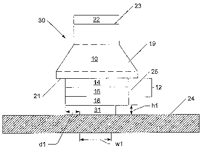
[0026] FIG. I illustrates an LED chip having a shaped substrate. Specifically,
the LED chip 30 shown in FIG. 1 has a substrate 10 having a first surface 21
and a second surface 23. The active region 12 is formed by epitaxial layers
deposited on the first surface 21. An ohmic contact 18 is formed on p-type
region 16. An n-type electrode 22 is formed on second surface 23 of the
substrate 10. The epitaxial regions 14, 16 and the ohmic contact layer 18 are
etched to form a mesa isolation structure 25. Ohmic contact layer 18 may
comprise other metal layers such as barrier layers, adhesion layers and/or
mirror layers.
[0027] In some embodiments, the width of first surface 21 of the LED chip may
be approximately 300 pm or greater. In some embodiments, the width of the
mesa structure 25 may be approximately 250 pm or greater.
[0028] LED chip 30 further includes a metal pad 31 through which chip 30 may
be thermosonically or thermocompressively bonded to a submount 24. Pad 31
preferably comprises Au or a suitable metal alloy such as Au/Sn, Pb/Sn, Sn,
Sn/Ag. Thermosonic bonding utilizes a combination of heat, pressure and
ultrasonic vibration to bond the chip to the submount.
[0029] In one embodiment illustrated in FIG. 3A, bond pad 31 comprises a
generally cylindrical shape having a generally circular cross-section and
having
a height h1 of about 2 pm. The bond pad may have a diameter less than one
half the width of mesa 25. In one embodiment, the circular bond pad has a
diameter of 120 pm. In this embodiment, the volume of the bond pad may be
less than about 2.3x10"5 mm3. In some embodiments, the volume of metal in
the bond pad may be less than about 3x10"5 mm3. In other embodiments, the
volume of metal in the bond pad may be less than about 2.5x10⁻⁵ mm3. Thus,
the cylindrical bond pad illustrated in FIG. 3A may have a diameter of about
200 pm and a height of about 0.95 pm or less. In some embodiments, the
cylindrical bond pad illustrated in FIG. 3A may have a diameter of about 200
pm and a height of about 0.8 pm or less.
CA 02564309 2006-10-26
WO 2005/106497 PCT/US2005/014493
-8-
[0030] In other embodiments illustrated in FIG. 3B, bond pad 31 may comprise
a parallelepiped having a height of about 1.2 pm and a generally square cross-
section. A square bond pad may have a width of less than about 2/3 the width
of mesa 25. In one embodiment, the square bond pad may have a width of
about 150 pm, resulting in a volume of about 2.7x10⁻⁵ mm3. As with the
embodiment illustrated in FIG. 3A, in some embodiments the volume of metal
in the bond pad may be less than about 3x10⁻⁵ mm3, and in other
embodiments, the volume of metal in the bond pad may be less than about
2.5x10⁻⁵ mm3.
[0031] In other embodiments illustrated in FIG. 3C, the bond pad 31 comprises
a polyhedron having opposing parallel faces and a periphery in the shape of a
four-point star oriented such that the four points extend along the diagonals
of
the face of the chip. Other peripheral shapes are also possible and may be
desirable depending on the shape of the LED chip. In this case, the distance
from the edge of the bond pad to the edge of the mesa is preferably no less
than about 50 pm. In some embodiments, the bond pad may be between 1.5
and 2.0 pm thick. As with the embodiments illustrated in FIGs. 3A and 3B, in
some embodiments the volume of metal in the bond pad may be less than
about 3x10⁻⁵ mm3, and in other embodiments, the volume of metal in the bond
pad may be less than about 2.5x10"5 mm3.
[0032]ln yet other embodiments illustrated in FIG. 3D, the bond pad 31
comprises a polyhedron having opposing parallel faces and a periphery in the
shape of a cross having generally rectangular regions extending towards the
edges of the chip. In this case, the distance from the edge of the rectangular
regions of the bond pad to the edge of the mesa is preferably about 20 pm. In
some embodiments, the bond pad may be about 0.5 pm thick. In these
embodiments, the volume of metal in the bond pad may be less than about
3x10⁻⁵ mm3, and in other embodiments, the volume of metal in the bond pad
may be less than about 2.5x10"5 mm3.
[0033]When the chip is welded to the substrate, the bond pad melts partially
and deforms to a new size as illustrated in FIG. 2. In one embodiment, the
height, width and shape of the bond pad 31 formed prior to mounting the chip
CA 02564309 2006-10-26
WO 2005/106497 PCT/US2005/014493
-9-
are selected such that the total volume of material in the bond pad 31 is less
than the resulting volume between the ohmic contact layer 18 and the
submount 24 after thermosonic or thermocompression bonding using the
application of 30-70g of force. For example, in the embodiment illustrated in
FIG. 2, the volume of material in the bond pad 31 is less than the height h2
multiplied by the area of the mesa 25 (equal to w2 x w2).
[0034] In thermocompression or thermosonic bonding, the force applied to the
chip affects the bond strength between the chip and the submount. While a
lower applied force may result in less squeeze-out of solder, a lower force
may
also result in lower bond strength. Typically, bond strength is measured by
the
lateral shear strength of the bond between the chip and the submount. In some
applications, a shear strength of 140g may be acceptable. Greater shear
strength may be desirable. For example, for mounting a chip having lateral
dimensions on the order of 300 pm x 300 pm, a shear strength of 300 - 600 g
may be desired.
[0035] In the drawings and specification there have been disclosed
embodiments of the invention, and, although specific terms have been
employed, they have been used in a generic and descriptive sense only and
not for purposes of limitation.