Note: Descriptions are shown in the official language in which they were submitted.
CA 02564421 2006-10-26
DESCRIPTION
Method of Producing Carbon Nanostructure
Technical Field
The present invention relates to a method of producing a carbon nanostructure
which enables a carbon nano structure having a more even shape to be produced
stably
and at a high purity, and which can also reduce a production cost.
Background Art
A carbon nanotube, which is formed with carbon atoms arranged in a tubular
shape having a diameter of a nanometer level, has been receiving considerable
attention
in recent years as a carbon-based highly functional material having advantages
such as
high conductivity and mechanical strength. As one method of generating the
carbon
nanotube, a thermal decomposition method has been devised, in which therr
decomposition of a material gas such as an alcohol-based or hydrocarbon-based
gas is
performed in a heating furnace using a catalyst particle having a diameter of
a nanometer
level to grow a carbon crystal on the catalyst particle to form the carbon
nanotube.
The thermal decomposition method includes a method in which a base material is
made
to carry the catalyst particle by application or the like, or a method in
which a catalyst is
suspended in a vapor phase.
Japanese Patent Laying-Open No. 60-054998 (Patent Document 1), for example,
proposes a method of generating a vapor phase epitaxy carbon fiber in a
suspended state
by heating a mixed gas including a gas of an organotransition metal compound,
a carrier
gas and a gas of an organic compound to 800-1300 C.
Japanese Patent Laying-Open No. 2001-020071 (Patent Document 2) proposes
a method of synthesizing a carbon nanotube including a step of forming a
catalyst metal
film on a substrate, a step of etching the catalyst metal film to form an
isolated nano-
sized catalyst metal particle, and a step of supplying a carbon source gas
into a
- 1 -
CA 02564421 2006-10-26
thermochemical vapor phase deposition device to grow a carbon nanotube on each
of
the isolated nano-sized catalyst metal particle by a thermochetnical vapor
phase
deposition method to form a plurality of carbon nanotubes aligned vertically
on the
substrate, in which the step of forming the isolated nano-sized catalyst metal
particle is
performed by a gas etching method using at least one eching gas selected from
the
group consisting of an ammonia gas, a hydrogen gas and a hydride gas after
thermal
decomposition.
Japanese Patent Laying-Open No. 2002-255519 (Patent Document 3) proposes
a method in which a hydrocarbon gas and a carrier gas are sent onto a base
including a
heat resistant porous carrier carrying dispersed fine catalyst particles to
vapor-phase
synthesize a monolayer carbon nanotube utilizing thermal decomposition of the
hydrocarbon gas.
Japanese Patent Laying-Open No. 2003-292315 (Patent Document 4) proposes
a method of producing a carbon nanotube on a surface of a metal by a chemical
vapor
phase epitaxy method with flowing a gas as a carbon source onto a heated
metal, which
is characterized in that a microcrystal of an oxide is generated beforehand on
the surface
of the metal to form minute projections and depressions on the surface of the
metal.
In a conventional method as described in each of Patent Documents 1-4,
however, a carbon substance such as amorphous carbon or graphite as an
impurity is
generated concurrently with an intended carbon nanotube during production of
the
carbon nanotube. In addition, generated carbon nanotubes have large variations
in
diameters, and it is difficult to stably produce even carbon nanotubes.
One of causes of the variations in diameters of carbon nanotubes is variations
in
sizes of catalyst particles. Since it is difficult to control a shape of a
catalyst particle
when the catalyst particle is formed by a chemical method such as heat
decomposition,
variations in shapes of catalyst particles themselves are generated.
Aggregation of
catalyst particles also causes variations in shapes. Shapes of carbon
nanotubes may
also vary due to variations in growth speeds of carbon crystals on the
catalyst particles.
- 2 -
CA 02564421 2011-11-25
In addition, a carbon nanotube having a large fiber length cannot be easily
generated using the catalyst particle.
Patent Document 1: Japanese Patent Laying-Open No. 60-054998
Patent Document 2: Japanese Patent Laying-Open No. 2001-020071
Patent Document 3: Japanese Patent Laying-Open No. 2002-255519
Patent Document 4: Japanese Patent Laying-Open No. 2003-292315
Disclosure of the Invention
An object of the present invention is to provide a method of producing a
carbon
nanostructure which solves the above-described problems, can increase evenness
of a
shape and a purity of the carbon nanostructure, and can reduce a production
cost.
Summary of the Invention
The present invention relates to a method of producing a carbon nanostructure
wherein a carbon crystal is grown by vapor phase epitaxy from a crystal growth
surface
of a catalyst base including a catalyst material, and the catalyst base is
formed by
diameter-reduction processing. The catalyst base is a columnar body which has
one end
surface as a crystal growth surface and the other end surface is a non-crystal
growth
surface. The catalyst material is formed successively from the crystal growth
surface to
the non-crystal growth surface. The catalyst base includes a non-catalyst
material on the
crystal growth surface and on at least a portion of the side surface of the
catalyst material.
The non-catalyst material does not have a catalytic function for growth of the
carbon
crystal.
In addition, a non-catalyst material is preferably formed on at least a
portion of
side surface of the aggregate. Furthermore, the catalyst structures preferably
have
variations of at most CV 10% in surface areas of the catalyst material on the
crystal
growth surface of the catalyst base formed as an aggregate.
The catalyst material is preferably formed with at least one of a member
selected
from the group consisting of Fe, Co, Mo, and Ni, and the non-catalyst material
is
preferably formed with Ag and/or an Ag-containing alloy.
- 3 -
CA 02564421 2006-10-26
Surface processing is preferably performed by at least one of oxidation,
nitriding
and carbonization to define an interface between the catalyst material and the
non-
catalyst material on the crystal growth surface.
A method of alternately stacking the catalyst material and the non-catalyst
material by a vapor phase method to form a catalyst base having a multilayer
structure is
also preferably used. With this, a catalyst base can be made which has the
catalyst
material in a spiral shape on the crystal growth surface.
The diameter-reduction processing of the present invention is preferably
performed by at least any of drawing, extrusion, rolling, and forging.
The diameter-reduction processing is preferably performed such that, an
outside
diameter of a solid or hollow catalyst material after the diameter-reduction
processing
becomes at least 1 > 10-6 % and at most 1 % of that before the diameter-
reduction
processing.
In the catalyst base used in the present invention, the catalyst material
preferably
has a multilayer structure on the crystal growth surface. Alternatively, the
catalyst
material preferably has at least any of a round shape, a ring-like shape, a
polygonal
shape, a spiral shape, a waved shape, and a branching shape on the crystal
growth
surface.
In the present invention, surface processing is preferably performed for the
catalyst material of the catalyst base used. In particular, mechanical
polishing and/or
sputtering is preferably performed.
Processing for entering an ion in the crystal growth surface is preferably
performed before and/or after the surface processing for the catalyst material
of the
catalyst base to prevent surface disorder of the crystal growth surface due to
the
mechanical polishing and/or sputtering.
The method of producing according to the present invention preferably includes
the steps of supplying carbon from a non-crystal growth surface of the
catalyst base to
set at least a portion of carbon in the catalyst material to a saturated
state, and growing
- 4 -
CA 02564421 2006-10-26
a carbon crystal from the crystal growth surface.
In the present invention, a reducing gas is preferably brought into contact
with at
least the crystal growth surface of the catalyst material before or during
growth of the
carbon crystal.
In addition, an ionized material gas and/or carbon is preferably brought into
contact with the catalyst base.
Effects of the Invention
Since a catalyst base including a catalyst material is formed by diameter-
reduction processing in the present invention, a crystal growth surface having
a desired
shape and an even size can be efficiently formed. With this, a carbon
nanostructure
having a shape reflecting a shape of the crystal growth surface can be
produced stably
and at a high purity. In addition, the catalyst base used in the present
invention can be
formed as a columnar body exposing the catalyst material on the crystal growth
surface
and a non-crystal growth surface. In this situation, carbon of a higher
concentration
can be absorbed from the non-crystal growth surface into the catalyst
material, which
increases production efficiency of the carbon nanostructure and can
effectively suppress
generation of an impurity.
Brief Description of the Drawings
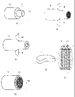
Fig. 1 shows an example of a method of making a catalyst base used in the
present invention.
Fig. 2 shows an example of a method of making a catalyst base having a
multilayer structure which is used in the present invention.
Fig. 3 is a cross-sectional view of a crystal growth surface of a catalyst
base
having a multilayer ring structure which is used in the present invention.
Fig. 4 is a cross-sectional view of a crystal growth surface of a catalyst
base
having a waved structure which is used in the present invention.
Fig. 5 shows an example of a production device of a carbon nanostructure.
Fig. 6 shows an example of a construction of a catalyst base used in the
present
- 5 -
CA 02564421 2006-10-26
=
invention.
Fig. 7 shows an example of a production device of a carbon nanostructure which
includes a plasma cementation device.
Description of the Reference Signs
11, 204, 31, 41, 52, 62, 72: catalyst material, 12, 15, 201, 205, 207, 210,
32, 42,
53, 63, 73: non-catalyst material, 13, 16, 206, 208, 211: composite material,
14, 209:
drawing dice, 17, 212, 54, 64, 74: catalyst base, 202, 203: deposition source,
51, 61, 71:
heat and pressure-resistant heating furnace tube, 55, 66: seal material, 56:
diaphragm,
57: crystal growth surface, 58, 67, 76: carbon nanostructure, 65: porous body,
75:
anode.
Best Modes for Carrying Out the Invention
The present invention is characterized in that, a catalyst base including a
catalyst
material is formed by diameter-reduction processing, and a carbon crystal is
generated
by vapor phase epitaxy from a crystal growth surface formed with the catalyst
material
on the catalyst base to produce a carbon nanostructure having a desired shape.
In the
present invention, diameter-reduction processing is performed for preferably
at least two
times for a catalyst material or a composite material of a catalyst material
and a non-
catalyst material which is prepared beforehand to decrease a diameter thereof
by plastic
deformation of the catalyst material and the non-catalyst material, which
enables making
of a catalyst base having a very small crystal growth surface of a nanometer
size with
high accuracy. With this, a shape of the crystal growth surface can be
arbitrarily set
according to a desired shape of a carbon nanostructure such as a carbon
nanotube or a
carbon nanofiber.
A solid or hollow, thin line-shaped or rod-shaped catalyst material, for
example,
is preferably adopted to efficiently perform diameter-reduction processing
with high
accuracy. In this situation, it is preferable to repeatedly perform the
diameter-
reduction processing to form a catalyst material having a diameter of a
nanometer level,
which is then cut to a desired length to form a solid or hollow columnar body
having an
- 6 -
CA 02564421 2006-10-26
=
intended height, and an end surface of the columnar body, that is, at least
one cut
surface thereof is preferably made to be a crystal growth surface. The shape
of the
crystal growth surface can be arbitrarily controlled by changing a cross-
sectional shape
of the catalyst material provided to diameter-reduction processing, and carbon
nanostructures having various cross-sectional shapes can be produced. In the
present
invention, the diameter-reduction processing can be performed such that, an
outside
diameter of the catalyst material after the diameter-reduction processing
becomes, for
example, at most 1 % of that before the diameter-reduction processing,
especially within
a range of 1 x 10⁶ ¨ 1%. In this situation, the outside diameter of the
catalyst material
before the diameter-reduction processing is relatively large and a cross-
sectional shape is
easily designed. In addition, the catalyst material having the outside
diameter of a
nanometer level can be readily made by the diameter-reduction processing.
Though the catalyst base used in the present invention may be formed only with
the catalyst material, a non-catalyst material which does not have a
substantial catalytic
function for growth of a carbon crystal is preferably formed on at least a
portion of a
side surface of the catalyst material which is formed as a columnar body
having a crystal
growth surface as an end surface. In this situation, spreading of the carbon
crystal in a
direction of the crystal growth surface is prevented by presence of the non-
catalyst
material, and a growth direction of the carbon crystal is controlled to enable
production
of a carbon nanostructure having a more even shape.
A material generally used as a catalyst in production of a carbon
nanostructure
can be used as the catalyst material. More specifically, a metal or an alloy
including at
least one member selected from Fe, Co, Mo, Ni, In, and Sn can be used. These
materials can be used singly or in combination of at least two kinds. Among
these, Fe,
Co and Fe-Co alloy materials are suitable because they substantially do not
form alloy or
the like with Ag which is preferably used as the non-catalyst material as
described below,
and because they are catalysts which are not easily deteriorated.
The non-catalyst material may be any material which does not have a
substantial
- 7 -
CA 02564421 2006-10-26
catalytic function for growth of a carbon crystal. More specifically, a metal
or an alloy
including at least one member selected from Ag, Au, Ru, Rh, Pd, Os, Ir, and Pt
is
preferably used. Among these, Ag and an Ag-containing alloy are suitable
because
they are relatively inexpensive, can be processed easily, and are chemically
stable. As
the Ag-containing alloy, alloys such as Ag-Pd, Ag-Pt and Ag-Au alloys can be
preferably used.
When a catalyst base formed with a composite body of the catalyst material and
the non-catalyst material is used, the catalyst material and the non-catalyst
material
which substantially do not generate an alloy or cause a reaction when they
contact each
other and which have a low possibility of degrading a shape of the crystal
growth
surface are preferably used in combination. Such combination includes, for
example, a
combination of an oxide as the catalyst material and Ag or an Ag-containing
alloy as the
non-catalyst material, and a combination of a nitride as the catalyst material
and Ag or
an Ag-containing alloy as the non-catalyst material. In addition, a
combination of the
catalyst material formed with at least one member selected from Fe, Co, Mo,
Ni, In, and
Sn and the non-catalyst material formed with Ag and/or an Ag-containing alloy
is also
preferred.
The non-catalyst material preferably has a melting point higher than a
generation
temperature of the carbon nanostructure. In this situation, deformation of the
non-
catalyst material does not easily occur during crystal growth and a carbon
nanostructure
having an even shape can be generated.
In the present invention, a columnar catalyst base formed by arranging a
plurality
of columnar catalyst structures each formed with the catalyst material and the
non-
catalyst material, for example, can be preferably used to efficiently generate
the carbon
nanostructure. Production efficiency of the carbon nanostructure can be
increased by
using the catalyst base formed with a plurality of catalyst structures.
When the catalyst base is formed as a columnar aggregate including an
arrangement of the plurality of catalyst structures each formed with the
catalyst material
- 8 -
CA 02564421 2006-10-26
=
and the non-catalyst material, it is preferable to further form the non-
catalyst material on
at least a portion of a side surface of the aggregate. In this situation,
unevenness of a
shape of the carbon nanostructure due to a generated carbon crystal spreading
in a
direction of the crystal growth surface is further suppressed by a
contribution of the
non-catalyst material formed on the side surface of the aggregate, in addition
to a
contribution of the non-catalyst material in each of the catalyst structures.
When the catalyst base is formed by arranging the plurality of catalyst
structures
each formed with the catalyst material and the non-catalyst material, the
catalyst
structures preferably have variations of at most CV 10% in surface areas of
the catalyst
material on the crystal growth surface. In this situation, evenness of a cross-
sectional
shape of the carbon nanostructure can be ensured with a sufficiently even
shape of the
crystal growth surface. A surface area of the catalyst material can be
calculated by, for
example, an image analysis based on a figure observation with an STM (scanning
tunneling microscope).
A reinforcing material for suppressing deformation of the catalyst base may be
formed in at least a portion of the catalyst base formed with the catalyst
material and the
non-catalyst material, preferably in at least a portion of aiperiphery of the
catalyst base.
In this situation, generation of a gap between the catalyst material and the
non-catalyst
material is suppressed by the reinforcing material and generation of carbon as
an
impurity from an interface between the catalyst material and the non-catalyst
material is
avoided, which can further increase evenness of the carbon nanostructure. As
the
reinforcing material, a material having a Young's modulus larger than that of
the catalyst
base formed with the catalyst material and the non-catalyst material in a
condition of
production of the carbon nanostructure is preferably used. In particular, a
material
having heat resistance higher than that of the non-catalyst material is
preferably used.
More specifically, a heat-resistant high-strength metal such as tungsten
carbide, ceramics
or Inconel, for example, is used.
A method which enables reduction of a diameter by plastic deformation of the
- 9 -
CA 02564421 2006-10-26
catalyst material or the composite material of the catalyst material and the
non-catalyst
material can be adopted as a method of diameter-reduction processing in the
present
invention. More specifically, at least one processing selected from drawing,
extrusion,
rolling, and forging is preferred. When two or more of the processings are
performed
in combination, a method of thinning a material formed in a rod-like shape to
a degree
by rolling and then further reducing a diameter thereof by drawing or
extrusion, or a
method of embossing to apply a stress in a direction of a radius of a rod-
shaped material
by forging for thinning to a degree and then further reducing a diameter
thereof by
drawing or extrusion, for example, can be adopted. When the diameter-reduction
processing is performed, it is preferable to select a processing condition as
appropriate
not to cause rapid plastic deformation in order to prevent deterioration of
physical
properties of the material.
A method of making the catalyst base used in the present invention will now be
described referring to the drawing. Fig. 1 shows an example of a method of
making
the catalyst base used in the present invention. First, as shown in Fig. 1(A),
a pipe-
shaped non-catalyst material 12 is filled with a rod-shaped catalyst material
11 to obtain
a composite material 13. Then, as shown in Fig. 1(B), composite material 13 is
passed
through a drawing dice 14 for drawing to cause diameter-reduction with plastic
deformation of composite material 13, and is further used to fill a pipe-
shaped non-
catalyst material 15 to obtain a composite material 16, as shown in Fig. 1(C).
As
shown in Fig. 1(D), composite material 16 obtained is passed through drawing
dice 14
again for diameter-reduction with plastic deformation. By repeating filling
and
diameter-reduction operations as described above, a columnar aggregate
including an
arrangement of a plurality of catalyst materials 11 each having a diameter of
at most 10
nm, for example, is obtained. The aggregate is cut to a prescribed length and
a cut
surface thereof is polished to finally obtain a catalyst base 17 as shown in
Figs. 1(E) and
l(F) which is a columnar body formed with the plurality of catalyst materials
11, which
columnar body has one end surface as a crystal growth surface and the other
end surface
- 10 -
CA 02564421 2006-10-26
=
as a non-crystal growth surface (herein, portions enclosed with dotted lines
in Figs. 1(E)
and 1(F) indicate an identical region). On each of the crystal growth surface
and the
non-crystal growth surface of catalyst base 17 shown in Fig. 1(E), catalyst
material 11
has a round shape. A catalyst material layer may be provided, for example, on
the non-
crystal growth surface of catalyst base 17. When the catalyst base having a
construction as such is used and a material gas is brought into contact with
the non-
crystal growth surface, carbon of a high concentration dissolves in catalyst
material 11
with a contribution of the catalyst material layer having a large surface
area, and since
carbon of the high concentration is supplied to the crystal growth surface, a
speed of
generation of the carbon nanostructure can be increased.
In the catalyst base used in the present invention, the catalyst material
preferably
has at least any of a round shape, a ring-like shape, a spiral shape, a
polygonal shape, a
waved shape, and a branching shape on the crystal growth surface. It is also
preferable
to form the catalyst material to have a multilayer structure on the crystal
growth surface.
In this situation, a shape of the crystal growth surface is reflected to a
cross section of
the carbon nanostructure generated, and a carbon nanostructure having a
monolayer or
multilayer spiral shape or ring-like shape, for example, can be arbitrarily
generated. As
a method of forming a multilayer structure or a ring structure on the crystal
growth
surface, a method of interposing the non-catalyst material between monolayer
or
multilayer catalyst materials by a method of alternately stacking the catalyst
material and
the non-catalyst material by a vapor phase method, or by a method of
performing, once
or at least two times, a step of filling the catalyst material or the non-
catalyst material
prepared to have a pipe-like shape with the catalyst material or the non-
catalyst material
prepared to have a rod-like shape, for example, can be preferably adopted. In
the
catalyst base shown in Fig. I, though catalyst material 11 on the crystal
growth surface
has a round shape because rod-shaped catalyst material 11 is used, when the
non-
catalyst material is used in place of catalyst material 11 and the catalyst
material is used
in place of non-catalyst material 12, for example, a catalyst base having a
ring-shaped
- 11 -
CA 02564421 2006-10-26
crystal growth surface can be made.
Fig. 2 shows an example of a method of making a catalyst base having a
multilayer structure which is used in the present invention. As shown in Fig.
2(A), a
non-catalyst material 201 is rotated in a direction of an arrow, and a non-
catalyst
material and a catalyst material are concurrently deposited on non-catalyst
material 201
from a deposition source 202 for depositing the non-catalyst material and a
deposition
source 203 for depositing the catalyst material. With this, as shown in Fig.
2(B), a
composite material 206 having a multilayer structure including a catalyst
material 204
and a non-catalyst material 205 formed in a spiral shape on a periphery of non-
catalyst
material 201 is obtained. Then, as shown in Fig. 2(C), a pipe-shaped non-
catalyst
material 207 is filled with composite material 206 to obtain a composite
material 208.
As shown in Fig. 2(D), composite material 208 is passed through a drawing dice
209 to
cause diameter-reduction with plastic deformation and, furthermore, a non-
catalyst
material 210 is filled with composite material 208 to obtain a composite
material 211, as
shown in Fig. 2(E). As shown in Fig. 2(F), composite material 211 is passed
through
drawing dice 209 to cause diameter-reduction with plastic deformation and,
finally, a
catalyst base 212 as shown in Figs. 2(G) and 2(H) which is a columnar body
formed
with a plurality of composite materials 206 each having the catalyst material
formed in a
spiral shape can be made, which columnar body has one end surface as a crystal
growth
surface (herein, portions enclosed with dotted lines in Figs. 2(G) and 2(H)
indicate an
identical region).
A number or thicknesses of layers of the multilayer structure can be readily
controlled by controlling an amount of deposition of the catalyst material
and/or the
non-catalyst material, a rotation speed of non-catalyst material 201 or the
like in a step
shown in Fig. 2(A). In addition, a layered structure may be arbitrarily
controlled by
adjusting a deposition start time and/or a deposition end time of the catalyst
material or
the non-catalyst material from deposition sources 202 and 203. It is to be
noted that,
the catalyst material may be used in place of non-catalyst material 201
according to a
- 12 -
CA 02564421 2006-10-26
desired structure of a carbon nano structure. In this situation, the catalyst
material on
the crystal growth surface has a shape having a filled center portion.
Fig. 3 is a cross-sectional view of a crystal growth surface of a catalyst
base
having a multilayer ring structure which is used in the present invention. In
the catalyst
base shown in Fig. 3, a catalyst material 31 and a non-catalyst material 32
are formed to
have a layered structure and catalyst material 31 has a crystal growth surface
of a
multilayer ring-like shape. Fig. 4 is a cross-sectional view of a crystal
growth surface
of a catalyst base having a waved structure which is used in the present
invention. In
the catalyst base shown in Fig. 4, a catalyst material 41 is formed on a
periphery of a
non-catalyst material 42 and catalyst material 41 has a crystal growth surface
of a waved
ring-like shape.
When a rod-shaped and/or pipe-shaped catalyst material or composite material
of the catalyst material and the non-catalyst material is used, it is
preferable to cut the
catalyst material or the composite material subjected to diameter-reduction
processing
to a desired length, and polish cut surfaces (end surfaces) thereof by, for
example, ion
milling or laser beam processing to obtain a columnar catalyst base having one
of the
end surfaces as a crystal growth surface and the other as a non-crystal growth
surface.
When the catalyst base is formed as a columnar body, a thickness of the
catalyst
base, that is, a height of the columnar body is preferably set to, for
example, about I-
1000 1..un. The catalyst base is readily prepared when the thickness of the
catalyst base
is at least 1 p,m, and carbon is stably supplied to the crystal growth surface
even if a
material gas is brought into contact with only the non-crystal growth surface
when the
thickness is at most 1000 p.m. When the thickness of the catalyst base is
relatively
small, however, deformation of the catalyst base may occur depending on a
production
condition such as a condition of supply of an atmospheric gas. In this
situation, it is
preferable to affix a porous body formed with a non-catalyst material to the
non-crystal
growth surface of the catalyst base, supply a material gas from a side of the
porous body,
and grow a carbon crystal from the crystal growth surface. With this,
deformation of
- 13 -
CA 02564421 2006-10-26
the catalyst base can be prevented without decreasing an amount of supply of
carbon
into the catalyst material. Furthermore, it is preferable to reinforce the
catalyst material
by, for example, forming a film on the non-crystal growth surface, as shown in
Fig. 5.
In the present invention, surface processing by mechanical polishing and/or
sputtering is preferably performed beforehand for the crystal growth surface
in order to
increase evenness of a shape of a generated carbon nanostructure by cleaning
and
smoothing of the crystal growth surface. At least one kind selected from a
plasma, an
ion beam and a laser beam is preferably used in the sputtering since the
crystal growth
surface can be processed to be more smooth with high processing efficiency.
Furthermore, a cluster ion beam and an ultrashort pulse laser are preferably
used as the
ion beam and the laser beam, respectively.
Furthermore, it is preferable to enter an ion in the crystal growth surface
before
and/or after the surface processing to resolve surface disorder of the crystal
growth
surface due to the mechanical polishing and/or sputtering. As a method of
entering the
ion, a method such as a cementation method or a plasma method, for example,
can be
adopted.
In addition, in order to further resolve the surface disorder of the crystal
growth
surface and define an interface between the catalyst material and the non-
catalyst
material, at least one processing selected from oxidation, nitriding and
carbonization is
preferably performed for the crystal growth surface. With this, generation of
an
impurity other than a desired carbon nanostructure can be suppressed and
production
efficiency of the carbon nanostructure can be increased. Oxidation, for
example, can
be performed by heat treatment in an oxygen atmosphere or the like.
Reactivation processing is preferably performed for the crystal growth surface
after generation of the carbon nanostructure using at least one processing
selected from,
for example, chemical polishing, physical polishing and sputtering. The
catalyst base
can be reused by reactivation of the crystal growth surface, and a production
cost can be
reduced.
- 14 -
CA 02564421 2006-10-26
In the present invention, a gas generally used for producing a carbon
nanostructure including a hydrocarbon-based gas such as a propane gas, an
ethylene gas
or an acetylene gas, an alcohol-based gas such as a methyl alcohol gas or an
ethyl
alcohol gas, or carbon monoxide can be used as a material gas for growing the
carbon
nanostructure. When a material having a relatively low deformation temperature
is
used as a material forming the catalyst base, for example, the alcohol-based
gas is
preferably used which enables generation of the carbon nanostructure at a
lower
temperature.
Since the carbon nanostructure generated may be degraded by a hydrogen gas or
the like, a gas which does not substantially deteriorate the carbon crystal
generated is
preferably supplied as a carrier gas to a portion near the crystal growth
surface. A
preferable carrier gas includes, for example, an inert gas such as argon or
nitrogen.
Though a condition of supply of a gas brought into contact with the catalyst
base
may be the same for the portion near the crystal growth surface and a portion
near the
non-crystal growth surface, the condition is preferably made different for
each portion
so that dissolving of carbon into the catalyst material and precipitation of
the carbon
crystal are controlled to occur in separate regions of a surface of the
catalyst base.
When a material gas is brought into contact with the portion near the non-
crystal growth
surface and a carrier gas not including a carbon source is brought into
contact with the
portion near the crystal growth surface, for example, only carbon which is
supplied from
the non-crystal growth surface, moves inside the catalyst base and reaches the
crystal
growth surface is supplied to the crystal growth surface. Therefore,
generation of an
impurity, which is readily generated when carbon exists in an atmospheric gas
near the
crystal growth surface, can be suppressed and the carbon nanostructure with a
higher
purity can be generated. Besides, high production efficiency can be attained
because
carbon of a high concentration is always supplied to the crystal growth
surface. In this
situation, since the material gas is not supplied to the portion near the
crystal growth
surface and a pressure due to entering of carbon is not applied to the crystal
growth
- 15 -
CA 02564421 2006-10-26
surface from a surface toward an internal portion of the catalyst material,
carbon is
supersaturated in the portion near the crystal growth surface and can
precipitate as a
carbon crystal.
Though only one kind of material gas or a combination of two kinds of gases,
that is, a material gas and a carrier gas, for example, can be adopted as a
gas used in the
present invention, gases of at least three kinds may be combined and used.
More
specifically, a combination for bringing a material gas into contact with the
catalyst
material in a region other than that near the crystal growth surface,
supplying a first
carrier gas for accelerating growth of the carbon nanostructure to the portion
near the
crystal growth surface, and further supplying a second carrier gas for moving
the carbon
nanostructure generated, or a combination of a gas for suppressing
precipitation of
carbon from a material gas itself or from a contact region between the
catalyst base and
the material gas and the material gas, for example, can be adopted.
In addition, when at least two kinds of atmospheric gases are supplied, the
atmospheric gases can be supplied to contact the catalyst base with different
pressures.
In this situation, a growth speed of the carbon nanostructure or a structure
such as a
number of layers in the generated carbon nanostructure can be controlled with
a
difference in pressures of the atmospheric gases.
Particularly, setting of a pressure of an atmospheric gas in a contact region
between the catalyst base and the material gas to be higher than a pressure of
an
atmospheric gas near the crystal growth surface is preferable because carbon
generated
by thermal decomposition of the material gas is absorbed into the catalyst
material more
efficiently.
In addition, at least one kind of the atmospheric gases is preferably supplied
to
contact the catalyst base with a pressure of at least an atmospheric pressure.
When the
material gas contacts the catalyst base with the pressure of at least the
atmospheric
pressure, carbon is absorbed into the catalyst material more efficiently. In
addition,
deformation of the catalyst base can be suppressed by setting a pressure of
the
- 16 -
CA 02564421 2006-10-26
atmospheric gas near the crystal growth surface to be equal to a pressure of
the
atmospheric gas on a side of supply of the material gas.
It is also preferable to set a surface area of the catalyst material
contacting the
material gas on a surface of the catalyst base to be larger than a surface
area of the
crystal growth surface. In this situation, production efficiency of the carbon
nanostructure is increased because carbon of a higher concentration which is
generated
by thermal decomposition of the material gas is supplied to the crystal growth
surface.
In the present invention, a reducing gas is preferably brought into contact
with at
least the crystal growth surface of the catalyst material before or during
growth of the
carbon crystal. The crystal growth surface of the catalyst material may be
oxidized
during the steps of making the catalyst base, surface-processing the crystal
growth
surface, and the like. With contacting the reducing gas, a metal oxide layer
on the
crystal growth surface can be removed and the carbon nanostructure can be
generated in
a more even shape. As a method of contacting the reducing gas, for example, a
method of supplying an atmospheric gas including a hydrogen gas or the like to
bring
the atmospheric gas into contact with the crystal growth surface can be
adopted.
Though a temperature for generating the carbon nanostructure in the present
invention is not specifically limited and can be selected as required
according to
properties of an applied catalyst base, a kind of a material gas or the like,
the
temperature can be set to, for example, about 500-960 C. Depending on a
production
condition, however, the catalyst material may be deformed or may be
deteriorated by an
impurity attached to a surface of the catalyst material, which forms an alloy
or a
compound of the catalyst material and decreases a catalyst activity. Since
reliable
growth of the carbon nanostructure having a desired shape becomes difficult
when the
crystal growth surface of the catalyst material is deformed or deteriorated,
the
temperature for generating the carbon nanostructure is preferably set to at
most a
temperature which does not cause deformation or deterioration of the catalyst
base.
When the catalyst material including Fe is used, for example, the temperature
for
- 17 -
CA 02564421 2006-10-26
=
generating the carbon nanostructure is preferably set to at least an A1
transformation
temperature of Fe (iron) (for example, 723 C which is an A1 transformation
temperature of pure iron), especially to at least 850 C.
A method of producing a carbon nanostructure according to the present
invention preferably includes the steps of supplying carbon from a side of the
non-crystal
growth surface of the catalyst base to set at least a portion of carbon in the
catalyst
material to a saturated state, and growing a carbon crystal from the crystal
growth
surface. In this situation, since the carbon crystal is grown with carbon of a
high
concentration supplied to the crystal growth surface, evenness of a shape of
the carbon
nanostructure obtained and production efficiency can be increased. More
specifically,
a method including a step of setting a temperature near the crystal growth
surface to be
higher than a temperature for generating the carbon crystal while bringing a
material gas
into contact with the non-crystal growth surface to supply carbon into the
catalyst base
to set carbon in the catalyst material to a saturated state, and a subsequent
step of
decreasing the temperature near the crystal growth surface to be at most the
temperature for generating the carbon crystal to grow the carbon crystal from
the crystal
growth surface, for example, can be preferably adopted. The temperature near
the
crystal growth surface can be controlled by, for example, providing a heat
source near
the crystal growth surface.
The method of producing a carbon nanostructure in the present invention will
now be described. Fig. 5 shows an example of a production device of a carbon
nanostructure. In a heat and pressure-resistant heating furnace tube 51
including an
electric furnace as a heating device, a gas introduction and exhaust system, a
growth
temperature control system, a vacuum control system, a gas flowmeter, and the
like, a
catalyst base 54 formed with a catalyst material 52 and a non-catalyst
material 53 is
inserted, and catalyst base 54 is fixed to heat and pressure-resistant heating
furnace tube
51 with a seal material 55 filling a gap therebetween. Heat and pressure-
resistant
heating furnace tube 51 is separated into a space of a crystal growth surface
side and a
- 18 -
CA 02564421 2006-10-26
=
space of a non-crystal growth surface side with catalyst base 54 and seal
material 55.
In the space of the non-crystal growth surface side, a diaphragm 56, for
example, is
provided to supply a material gas so as to flow in a direction of an arrow. A
carrier
gas is supplied to the space of the crystal growth surface side. Carbon
generated by
thermal decomposition of the material gas supplied to the space of the non-
crystal
growth surface side moves inside catalyst material 52 in catalyst base 54,
reaches a
crystal growth surface 57 and precipitates from crystal growth surface 57 as a
carbon
crystal to grow a carbon nanostructure 58.
Fig. 6 shows an example of a construction of a catalyst base used in the
present
invention. In a heat and pressure-resistant heating furnace tube 61 including
an electric
furnace as a heating device, a gas introduction and exhaust system, a growth
temperature control system, a vacuum control system, a gas flowmeter, and the
like, a
catalyst base 64 formed with a catalyst material 62 and a non-catalyst
material 63 is
inserted. A porous body 65 formed with a non-catalyst material is formed to
contact a
non-crystal growth surface side of catalyst base 64, and catalyst base 64 is
fixed to heat
and pressure-resistant heating furnace tube 61 with a seal material 66. Heat
and
pressure-resistant heating furnace tube 61 is separated into a space of a
crystal growth
surface side and a space of the non-crystal growth surface side with catalyst
base 64 and
seal material 66 filling a gap. A material gas is supplied to the space of the
non-crystal
growth surface side in a flow in a direction of an arrow, and carbon generated
by
thermal decomposition of the material gas passes through a pore portion of
porous body
65, moves inside catalyst material 62 in catalyst base 64, reaches a crystal
growth
surface and precipitates as a carbon crystal to grow a carbon nanostructure
67.
In the present invention, it is also preferable to ionize a material gas
containing
carbon and bring it into contact with the catalyst material in order to
generate the carbon
nanostructure more efficiently. By ionizing the material gas and accelerating
ionized
carbon with an electric field to allow collision thereof with the catalyst
material,
solubility of carbon to the catalyst material can be increased and carbon can
penetrate to
- 19-
CA 02564421 2006-10-26
a deeper region of the catalyst material from a contact surface between the
material gas
and the catalyst material. With this, carbon of a high concentration is
supplied to the
crystal growth surface and production efficiency of the carbon nanostructure
can be
increased. Plasma cementation, for example, can be adopted as a method of
ionizing
the material gas and bringing it into contact with the catalyst material. For
the plasma
cementation, for example, a method of applying a voltage between a furnace
tube
supplied with a material gas formed with a gas such as a mixed gas of a gas
containing a
carbon source and a carrier gas and the catalyst base to cause glow discharge
and
generating plasma of the material gas to ionize the material gas can be
adopted.
Fig. 7 shows an example of a production device of a carbon nanostructure which
includes a plasma cementation device. In the production device formed with a
heat and
pressure-resistant heating furnace tube 71 including an electric furnace as a
heating
device, a gas introduction and exhaust system, a growth temperature control
system, a
vacuum control system, a gas flowmeter, and the like, a catalyst base 74
formed with a
catalyst material 72 and a non-catalyst material 73 is inserted, and a space
formed with
heat and pressure-resistant heating furnace tube 71 is separated into a space
of a crystal
growth surface side and a space of a non-crystal growth surface side with
catalyst base
74. An anode 75 is arranged on the non-crystal growth surface side. As
an example,
a mixed gas including a propane gas, a methane gas, an ethylene gas, a
hydrogen gas, an
argon gas, or the like is supplied as a material gas to the space of the non-
crystal growth
surface side, catalyst base 74 is used as a cathode to apply a voltage between
anode 75
and catalyst base 74 to generate plasma with glow discharge, and carbon
generated by
decomposition of the material gas is supplied in an ionized state to the non-
crystal
growth surface.
The production device of a carbon nanostructure used in the present invention
may have a construction provided with, for example, a supply mechanism for a
purified
gas to enable purification of a material gas containing a decomposed gas or
the like after
generation of the carbon nanostructure. In addition, it is preferable to
electrify the
- 20 -
CA 02564421 2006-10-26
carbon nanostructure generated in the present invention and collect it with
force of static
electricity or the like.
The carbon nanostructure produced with the method of the present invention has
an even shape and is highly pure, which can be suitably applied to various
uses such as
an electronic circuit, a high-strength composite material, an electric wire
material, and a
cushion material.
<Examples>
Though the present invention will be described in more detail with examples,
the
present invention is not limited thereto.
(Example 1)
(1) Making of Catalyst base
In this example, a catalyst base was made by a method indicated in Fig. 1.
Composite material 13 (Fig. 1(A)), which was obtained by inserting an Fe
(iron) rod as
catalyst material 11 having an outside diameter of 40 mm into an Ag (silver)
pipe as
non-catalyst material 12 having an outside diameter of 60 mm and an inside
diameter of
40 mm, was subjected to wiredrawing with drawing dice 14 until an outside
diameter
thereof became 1.2 mm to obtain a wire 1 (Fig. 1(B)). Wire 1 was cut at every
length
of 1 m and bundled together to fill an Ag pipe as non-catalyst material 15
having an
outside diameter of 60 mm and an inside diameter of 40 mm, while spacers of Ag
were
used to fill gaps to avoid generation of a cavity, to form composite material
16 (Fig.
1(C)). Composite material 16 was passed through drawing dice 14 for
wiredrawing
until a diameter thereof became 1.2 mm to obtain a wire 2 (Fig. 1(D)). The
step of
obtaining wire 2 from wire 1 was repeated and, finally, an aggregate having a
diameter
of 30 mm was obtained which was formed with a bundle of a plurality of
catalyst
structures each formed with the catalyst material and the non-catalyst
material, in which
an outside diameter of Fe was set to 3 nm. The aggregate was cut to have a
length of
1 mm, and cut surfaces of both ends (both end surfaces) were polished by
buffing.
Lateral sputtering of the both end surfaces was performed using a cluster ion
-21 -
CA 02564421 2006-10-26
beam so that a structure of an Fe portion as the catalyst material was exposed
on the
both end surfaces in a round shape to make catalyst base 17 having a large
number of Fe
portions as catalyst materials 11 arranged in Ag portions as non-catalyst
materials 12
(Fig. 1(E)).
A crystal growth surface within a range of 0.11..tm square randomly selected
from the catalyst base formed was observed with a scanning electron microscope
to
calculate a cross-sectional area of the catalyst material in each catalyst
structure, and
variations in cross-sectional areas in the catalyst structures were obtained
with the
following expression.
CV (%) = standard deviation of all measured values/average value of all
measured values x 100
As a result, the variations in the cross-sectional areas of the catalyst
materials on
the crystal growth surface was at most 5 % in CV (%).
(2) Production of Carbon Nanostructure
A carbon nanotube as a carbon nanostructure was produced using the catalyst
base obtained as above. The catalyst base formed with the catalyst material
and the
non-catalyst material was inserted into a heat and pressure-resistant heating
furnace tube
including an electric furnace as a heating device, a gas introduction and
exhaust system,
a growth temperature control system, a vacuum control system, a gas flowmeter,
and
the like. While flowing an argon gas in the heat and pressure-resistant
heating furnace
tube, a temperature inside the heat and pressure-resistant heating furnace
tube was set to
850 C. After leaving for 1 hour with flowing an ethanol gas, the temperature
was
further gradually decreased to 500 C, and then supply of the ethanol gas was
stopped,
which was followed by cooling to a room temperature.
As a result, generation of fibrous carbon from the crystal growth surface was
recognized. When the catalyst base and the generated fibrous carbon were
observed
with the scanning electron microscope, it was ensured that the fibrous carbon
was
growing from the crystal growth surface of the catalyst material. When the
fibrous
- 22 -
CA 02564421 2006-10-26
carbon was further observed with a transmission electron microscope, it was
ensured
that the fibrous carbon was a carbon nanotube and an impurity such as
amorphous
carbon, graphite or the catalyst material was hardly included.
After observation with the electron microscope, the catalyst base was entered
into the heat and pressure-resistant heating furnace tube and an attempt was
made to
generate the carbon nanotube again in a condition similar to that described
above, but
the carbon nanotube was not generated due to contamination of a surface of the
catalyst
base and the like. Therefore, sputtering of the crystal growth surface with an
excimer
laser was performed and, thereafter, an attempt was made to generate the
carbon
nanotube again in the condition similar to that described above. As a result,
the carbon
nanotube could be generated.
(Example 2)
(1) Making of Catalyst base
In an Ag (silver) pipe having an outside diameter of 60 mm and an inside
diameter of 50 mm, an Fe (iron) pipe having an outside diameter of 50 mm and
an inside
diameter of 45 mm was inserted, and an Ag rod having an outside diameter of 45
mm
was further inserted therein. A composite metal material obtained was
subjected to
wiredrawing with a drawing dice until an outside diameter thereof became 1.2
mm to
obtain wire 1. Wire 1 was cut at every length of 1 m and bundled together to
fill an Ag
pipe having an outside diameter of 60 mm and an inside diameter of 40 mm,
while
spacers of Ag were used to fill gaps to avoid generation of a cavity, and the
Ag pipe was
subjected to wiredrawing with the drawing dice until a diameter thereof became
1.2 mm
to obtain wire 2. The step of obtaining wire 2 from wire 1 was repeated and,
finally, an
aggregate having a diameter of 30 mm was obtained which was formed with a
bundle of
a plurality of catalyst structures in which an outside diameter of Fe was set
to 7 nm.
The aggregate was cut to have a length of 0.2 mm, and cut surfaces of both
ends (both
end surfaces) were mechanically polished by buffing or the like.
Thereafter, a carbon ion is injected into a polished surface using an ion
- 23 -
CA 02564421 2006-10-26
implantation device. Planarization of the both end surfaces was performed
using an
excimer laser and a cluster ion beam so that a structure of an Fe portion as
the catalyst
material was exposed on the both end surfaces in a ring-like shape. Then, an
Fe film
having a thickness of 11..tm was formed on one end surface of the aggregate to
make a
catalyst base having the end surface on a side having the Fe film formed as a
non-crystal
growth surface and the end surface on a side not having the Fe film formed as
a crystal
growth surface.
(2) Production of Carbon Nanostructure
A carbon nanotube as a carbon nanostructure was produced with the production
device shown in Fig. 5 using the catalyst base obtained as above. Heat and
pressure-
resistant heating furnace tube 51 including the electric furnace as the
heating device, the
gas introduction and exhaust system, the growth temperature control system,
the
vacuum control system, the gas fiowmeter, and the like was separated into a
space of a
crystal growth surface side and a space of a non-crystal growth surface side
with
catalyst base 54 inserted and seal material 55. Catalyst material 52 was
exposed to
both of the spaces of the crystal growth surface side and the non-crystal
growth surface
side, and had a round shape having a diameter set to 7 am on the crystal
growth surface.
The Fe film as the catalyst material was exposed on whole surface of the non-
crystal
growth surface. While supplying an acetylene gas and a hydrogen gas to a side
of
catalyst base 54 having the Fe film formed, that is, to the non-crystal growth
surface side,
a temperature inside heat and pressure-resistant heating furnace tube 51 was
set to 870
C. On the other hand, an argon gas as a carrier gas was supplied to the
crystal growth
surface side.
As a result, generation of fibrous carbon from the crystal growth surface was
recognized. When catalyst base 54 and the generated fibrous carbon were
observed
with the scanning electron microscope, it was ensured that the fibrous carbon
was
growing from the crystal growth surface of the catalyst material. When the
fibrous
carbon was further observed with the transmission electron microscope, it was
ensured
- 24 -
CA 02564421 2006-10-26
that the fibrous carbon was a carbon nanotube and an impurity such as
amorphous
carbon, graphite or the catalyst material was hardly included.
After observation with the electron microscope, the catalyst base was entered
into heat and pressure-resistant heating furnace tube 51 and an attempt was
made to
generate the carbon nanotube again in a condition similar to that described
above, but
the carbon nanotube was not generated due to contamination of a surface of the
catalyst
base and the like. Therefore, sputtering of the crystal growth surface with a
cluster ion
beam was performed and, thereafter, an attempt was made to generate the carbon
nanotube again in the condition similar to that described above. As a result,
the carbon
nanotube could be generated.
(Example 3)
(1) Making of Catalyst base
In this example, a catalyst base was made by a method shown in Fig. 2. That
is,
while rotating an Ag rod as non-catalyst material 201 having an outside
diameter of 40
mm, Fe and Ag were concurrently deposited on a periphery of the Ag rod from
deposition sources 202 and 203 (Fig. 2(A)) to form composite material 206 in a
spiral
shape having respective 10 layers of Fe as catalyst materials 204 each having
a thickness
of 1 m and Ag layers as non-catalyst materials 205 each having a thickness of
5 1.1.m
(Fig. 2(B)). An Ag layer as non-catalyst material 207 was further formed to
make an
outside diameter of a periphery of a resulting composite material 208 become
60 mm
(Fig. 2(C)).
Composite material 208 obtained was passed through drawing dice 209 for
wiredrawing until an outside diameter thereof became 1.2 mm to obtain wire 1
(Fig.
2(D)). Wire 1 was cut at every length of 1 m and bundled together to fill an
Ag pipe as
non-catalyst material 210 having an outside diameter of 60 mm and an inside
diameter of
40 mm, while spacers of Ag were used to fill gaps to avoid generation of a
cavity, to
form composite material 211 (Fig. 2(E)). Composite material 211 obtained was
passed
through drawing dice 209 for wiredrawing until a diameter thereof became 1.2
mm to
- 25 -
CA 02564421 2006-10-26
obtain wire 2 (Fig. 2(F)). The step of obtaining wire 2 from wire 1 was
repeated and,
finally, an aggregate having a diameter of 10 mm was obtained which was formed
with a
bundle of a plurality of catalyst structures in which a thickness of each of
Fe layers was
set to 2 nm. The aggregate was cut to have a length of 0.5 mm, and cut
surfaces of
both ends (both end surfaces) were mechanically polished by buffing or the
like.
Planarization of the both end surfaces was performed using a cluster ion beam
so
that a structure of an Fe portion as the catalyst material was exposed on the
both end
surfaces in a spiral shape to make catalyst base 212 having a large number of
composite
materials 206 each having the catalyst material included in non-catalyst
material 207 (Fig.
2(G)).
(2) Production of Carbon Nanostructure
A carbon nanotube as a carbon nanostructure was produced with the production
device shown in Fig. 5 using the catalyst base obtained as above. Heat and
pressure-
resistant heating furnace tube 51 including the electric furnace as the
heating device, the
gas introduction and exhaust system, the growth temperature control system,
the
vacuum control system, the gas flowmeter, and the like was separated into a
space of a
crystal growth surface side and a space of a non-crystal growth surface side
with
catalyst base 54 inserted and seal material 55. While supplying an acetylene
gas
together with an argon gas to the space of the non-crystal growth surface
side, a
temperature inside heat and pressure-resistant heating furnace tube 51 was set
to 840 C.
On the other hand, an argon gas as a carrier gas was supplied to the space of
the crystal
growth surface side.
As a result, generation of fibrous carbon from the crystal growth surface was
recognized. When catalyst base 54 and the generated fibrous carbon were
observed
with the scanning electron microscope, it was ensured that the fibrous carbon
was
growing from the crystal growth surface of the catalyst material. When the
fibrous
carbon was further observed with the transmission electron microscope, it was
ensured
that the fibrous carbon was a carbon nanotube and an impurity such as
amorphous
- 26 -
CA 02564421 2006-10-26
carbon, graphite or the catalyst material was hardly included.
After observation with the electron microscope, catalyst base 54 was entered
into heat and pressure-resistant heating furnace tube 51 and an attempt was
made to
generate the carbon nanotube again in a condition similar to that described
above, but
the carbon nanotube was not generated due to contamination of a surface of the
catalyst
base and the like. Therefore, sputtering of the surface of the catalyst base
with a
cluster ion beam was performed and, thereafter, an attempt was made to
generate the
carbon nanotube again in the condition similar to that described above. As a
result, the
carbon nanotube could be generated.
(Example 4)
(1) Making of Catalyst base
In an Ag-Au (silver-gold) alloy pipe having an outside diameter of 60 mm and
an
inside diameter of 50 mm, an Fe (iron) pipe having an outside diameter of 50
mm and an
inside diameter of 45 mm was inserted, and an Ag-Au alloy rod having an
outside
diameter of 45 mm was further inserted therein. A composite material obtained
was
subjected to wiredrawing with a drawing dice until an outside diameter thereof
became
1.2 mm to obtain wire 1. Wire 1 was cut at every length of 1 m and bundled
together
to fill an Ag-Au pipe having an outside diameter of 60 mm and an inside
diameter of 40
mm, while spacers of an Ag-Au alloy were used to fill gaps to avoid generation
of a
cavity, and the Ag-Au pipe was subjected to wiredrawing with the drawing dice
until a
diameter thereof became 1.2 mm to obtain wire 2. The step of obtaining wire 2
from
wire 1 was repeated and, finally, an aggregate having a diameter of 5 mm was
obtained
which was formed with a bundle of a plurality of catalyst structures in which
an outside
diameter of Fe was set to 20 nm. The aggregate was cut to have a length of 2
mm, and
cut surfaces of both ends (both end surfaces) were mechanically polished by
buffing or
the like.
Planarization of the both end surfaces was performed using a cluster ion beam
or
the like so that an Fe portion as the catalyst material was exposed on the
both end
- 27 -
CA 02564421 2011-11-25
surfaces in a ring-like shape. Then, an Fe film having a thickness of 2 um was
formed
on one end surface to make a catalyst base having the end surface on a side
having the
Fe film formed as a non-crystal growth surface and the end surface on a side
not having
the Fe film formed as a crystal growth surface.
(2) Production of Carbon Nanostructure
A carbon nanotube as a carbon nanostructure was produced with the production
device shown in Fig. 5 using the catalyst base obtained as above. Heat and
pressure-
resistant heating furnace tube 51 including the electric furnace as the
heating device, the
gas introduction and exhaust system, the growth temperature control system,
the
vacuum control system, the gas flowmeter, and the like was separated into a
space of a
crystal growth surface side and a space of a non-crystal growth surface side
with
catalyst base 54 inserted and seal material 55. While flowing a mixed
atmospheric gas
containing an acetylene gas and an argon gas in a ratio of 1:4 and 1:5 atm in
the space of the
non-crystal growth surface side, a temperature inside heat and pressure-
resistant heating
furnace tube 51 was set to 960 C. On the other hand, an argon gas as a
carrier gas
was supplied to the crystal growth surface side. Thereafter, a ratio of supply
of an
acetylene gas was gradually decreased to zero while keeping a pressure of the
atmospheric gas.
As a result, generation of fibrous carbon from the crystal growth surface was
recognized. When catalyst base 54 and the generated fibrous carbon were
observed
with the scanning electron microscope, it was ensured that the fibrous carbon
was
growing from the crystal growth surface of the catalyst material. When the
fibrous
carbon was fiirther observed with the transmission electron microscope, it was
ensured
that the fibrous carbon was a carbon nanotube and an impurity such as
amorphous
carbon, graphite or the catalyst material was hardly included.
After observation with the electron microscope, catalyst base 54 was entered
into heat and pressure-resistant heating furnace tube Si and an attempt was
made to
generate the carbon nanotube again in a condition similar to that described
above, but
- 28 -
CA 02564421 2006-10-26
=
the carbon nanotube was not generated due to contamination of a surface of the
catalyst
base and the like. Therefore, sputtering of the surface of the catalyst base
with a
cluster ion beam was performed and, thereafter, an attempt was made to
generate the
carbon nanotube again in the condition similar to that described above. As a
result, the
carbon nanotube could be generated.
(Example 5)
(1) Making of Catalyst base
In an Ag (silver) pipe having an outside diameter of 60 mm and an inside
diameter of 50 mm, an Fe (iron) pipe having an outside diameter of 50 mm and
an inside
diameter of 45 mm was inserted, and an Ag rod having an outside diameter of 45
mm
was further inserted therein. A composite metal material obtained was
subjected to
wiredrawing with a drawing dice until an outside diameter thereof became 1.2
mm to
obtain wire 1. Wire 1 was cut at every length of 1 m and bundled together to
fill an Ag
pipe having an outside diameter of 60 mm and an inside diameter of 40 mm,
while
spacers of Ag were used to fill gaps to avoid generation of a cavity, and the
Ag pipe was
subjected to wiredrawing with the drawing dice until a diameter thereof became
1.2 mm
to obtain wire 2. The step of obtaining wire 2 from wire 1 was repeated and,
finally, an
aggregate having a diameter of 5 mm was obtained which was formed with a
bundle of a
plurality of catalyst structures in which an outside diameter of Fe was set to
12 nm.
The aggregate was cut, and cut surfaces of both ends (both end surfaces) were
mechanically polished by buffing or the like to obtain a thickness of 1 mm.
Planarization of the both end surfaces was performed using a cluster ion beam
or
the like so that a structure of an Fe portion as the catalyst material was
exposed on the
both end surfaces in a ring-like shape. Thereafter, a porous body made of Ag
having a
thickness of 3 mm and including a large number of pores of about 80 iml) was
subjected
to pressure welding to one end surface of a catalyst base to be a non-crystal
growth
surface, and was joined by heating or the like. Furthermore, irradiation with
an ion
beam or the like was performed for the other end surface to be a crystal
growth surface,
- 29 -
CA 02564421 2006-10-26
=
and the catalyst base was made to be a thin film until a length between the
both end
surfaces, that is, a thickness of the catalyst base became 80 pim. Finally,
planarization
of the crystal growth surface with a cluster ion beam was performed to remove
surface
roughness on the crystal growth surface of the catalyst material, and making
of the
catalyst base was completed.
(2) Production of Carbon Nanostructure
A carbon nanotube as a carbon nanostructure was produced using the
production device shown in Fig. 5 and the catalyst base obtained as above.
Heat and
pressure-resistant heating furnace tube 51 including the electric furnace as
the heating
device, the gas introduction and exhaust system, the growth temperature
control system,
the vacuum control system, the gas flowmeter, a plasma cementation device, and
the like
was separated into a space of a crystal growth surface side and a space of a
non-crystal
growth surface side with catalyst base 54 inserted and seal material 55. A
material gas
including an ethylene gas and a hydrogen gas mixed in a ratio of 1:2 was
introduced into
the space of the non-crystal growth surface side to be about 3 Torr (about 399
Pa) at
880 C. Heat and pressure-resistant heating furnace tube 51 was used as an
anode and
the catalyst base was used as a cathode to apply a DC voltage between both
electrodes
to cause glow discharge and generate plasma, and thereby carbon penetrated
from the
non-crystal growth surface into the catalyst material. On the other hand, a
mixed gas
of an argon gas and an H2 gas was introduced to the crystal growth surface
side and,
thereafter, supply of only the H2 gas was stopped.
As a result, generation of fibrous carbon from the crystal growth surface was
recognized. When catalyst base 54 and the generated fibrous carbon were
observed
with the scanning electron microscope, it was ensured that the fibrous carbon
was
growing from the crystal growth surface of the catalyst material. When the
fibrous
carbon was further observed with the transmission electron microscope, it was
ensured
that the fibrous carbon was a carbon nanotube and an impurity such as
amorphous
carbon, graphite or the catalyst material was hardly included.
- 30 -
CA 02564421 2006-10-26
(Example 6)
(1) Making of Catalyst base
In this example, a catalyst base having the construction shown in Fig. 6 was
used.
In an Ag (silver) pipe having an outside diameter of 36 mm and an inside
diameter of 9
mm, an Fe (iron) pipe (an Fe purity: about 4 N (99.99%)) having an outside
diameter of
9 mm and an inside diameter of 7 mm was inserted, and an Ag rod having an
outside
diameter of 7 mm was further inserted therein. A composite material obtained
was
subjected to wiredrawing with a drawing dice until an outside diameter thereof
became 2
mm to obtain wire 1. Wire 1 was cut at every length of 1 m and bundled
together to
fill an Ag pipe having an outside diameter of 36 mm and an inside diameter of
9 mm,
while spacers of Ag were used to fill gaps to avoid generation of a cavity,
and the Ag
pipe was subjected to wiredrawing with the drawing dice until a diameter
thereof
became about 1.2 mm to obtain wire 2. The step of obtaining wire 2 from wire 1
was
repeated to finally obtain an aggregate formed with a composite material
having Fe
penetrating through an Ag base material having a diameter of 20 mm which was
formed
with a bundle of a plurality of catalyst structures in which an outside
diameter of Fe was
set to 8 nm. The aggregate was cut, and cut surfaces of both ends (both end
surfaces)
were polished by buffing or the like to have a thickness of 50
Planarization of one end surface was performed using a cluster ion beam or the
like so as to expose a structure of an Fe portion as the catalyst material to
form a non-
crystal growth surface exposing the catalyst material in a ring-like shape.
Thereafter,
porous body 65 made of Ag having a thickness of 3 mm, which included holes of
about
200 pmcl) to form a lotus root-like shape, was subjected to pressure welding
to the non-
crystal growth surface of catalyst base 64, joined by heating or the like, and
further
reinforced with a base material made of WC (tungsten carbide). Finally,
planarization
of a crystal growth surface was performed using a cluster ion beam so as to
expose the
catalyst material in a ring-like shape to make catalyst base 64 having porous
body 65
formed thereon.
- 31 -
CA 02564421 2006-10-26
(2) Production of Carbon Nanostructure
A carbon nanotube as a carbon nanostructure was produced using the
production device shown in Fig. 6 and the catalyst base obtained as above.
Heat and
pressure-resistant heating furnace tube 61 including the heating device, the
gas
introduction and exhaust system, the growth temperature control system, the
vacuum
control system, the gas flowmeter, a plasma cementation device, and the like
was
separated into a space of a non-crystal growth surface side and a space of a
crystal
growth surface side with catalyst base 64 inserted and seal material 66.
A material gas including a hydrogen gas, a methane gas and an argon gas mixed
in a ratio of 2:1:2 was used to fill the space of the non-crystal growth
surface side to
attain about 4 Torr (about 532 Pa) at 860 C. The heat and pressure-resistant
heating
furnace tube was used as an anode and the catalyst base was used as a cathode
to apply
a DC voltage between both electrodes to cause glow discharge and generate
plasma,
and thereby carbon penetrated from the non-crystal growth surface side into
catalyst
material 62 via porous body 65. A carrier gas including a hydrogen gas and an
argon
gas was used to fill the space of the crystal growth surface side and, after
the carbon
nanotube as carbon nanostructure 67 was generated, supply of the hydrogen gas
was
stopped to supply only the argon gas to the space of the crystal growth
surface side.
As a result, generation of fibrous carbon from the crystal growth surface was
recognized. When the catalyst base and the generated fibrous carbon were
observed
with the scanning electron microscope, it was ensured that the fibrous carbon
was
growing from the crystal growth surface of the catalyst material. When the
fibrous
carbon was further observed with the transmission electron microscope, it was
ensured
that the fibrous carbon was a carbon nanotube and an impurity such as
amorphous
carbon, graphite or the catalyst material was hardly included.
In this example, during generation of the carbon nanotube, the hydrogen gas
was
supplied to the non-crystal growth surface and the crystal growth surface to
reduce an
iron oxide layer on an exposed surface of the catalyst material to accelerate
penetration
- 32 -
CA 02564421 2006-10-26
=
of carbon into the catalyst material and precipitation of a carbon crystal
from the crystal
growth surface.
(Example 7)
(1) Making of Catalyst base
In an Ag (silver) pipe having an outside diameter of 36 mm and an inside
diameter of 18 mm, an Fe (iron) pipe (an Fe purity: at least about 5 N
(99.999%))
having an outside diameter of 18 mm and an inside diameter of 14 mm was
inserted, and
an Ag rod having an outside diameter of 14 mm was further inserted therein. A
composite material obtained was subjected to wiredrawing with a drawing dice
until an
outside diameter thereof became 2 mm to obtain wire 1. Wire 1 was cut at every
length of 1 m and bundled together to fill an Ag pipe having an outside
diameter of 36
mm and an inside diameter of 18 mm, while spacers of Ag were used to fill gaps
to
avoid generation of a cavity, and the Ag pipe was subjected to wiredrawing
with the
drawing dice until a diameter thereof became 2 mm to obtain wire 2. The step
of
obtaining wire 2 from wire 1 was repeated to finally obtain an aggregate
formed with a
composite material having Fe penetrating through an Ag base material having a
diameter
of 20 mm which was formed with a bundle of a plurality of catalyst structures
in which
an outside diameter of Fe was set to about 8 nrn.
The aggregate was cut, and cut surfaces of both ends (both end surfaces) were
polished by buffing or the like to have a thickness of about 40 p.m.
Thereafter, a
cluster ion beam or the like was used to perform planarization of a non-
crystal growth
surface so as to expose the catalyst material in a ring-like shape, and an Fe
film having a
thickness of about 5 p.m was further formed on the non-crystal growth surface.
The
end surface to be a crystal grow surface was polished with the cluster ion
beam,
sputtering was performed to obtain a thickness of a catalyst base of about 10
p.m, and
planarization of the crystal grow surface was performed to expose the catalyst
material
in a ring-like shape. The catalyst base was made as above.
(2) Production of Carbon Nanostructure
- 33 -
CA 02564421 2006-10-26
A carbon nanotube as a carbon nanostructure was produced using the
production device shown in Fig. 7 and the catalyst base obtained as above. The
production device formed with heat and pressure-resistant heating furnace tube
71
including the electric furnace as the heating device, the gas introduction and
exhaust
system, the growth temperature control system, the vacuum control system, the
gas
flowmeter, a plasma cementation device, and the like was separated into a
space of a
non-crystal growth surface side and a space of a crystal growth surface side
with
catalyst base 74 inserted. Anode 75 was provided in the space of the non-
crystal
growth surface side. Catalyst material 72 was exposed on the non-crystal
growth
surface side and the crystal growth surface side. A temperature inside the
production
device was set to 850 C, a DC voltage was applied between anode 75 and
catalyst base
74 set as a cathode, and a material gas including a methane gas, a propane
gas, a
hydrogen gas, and an argon gas mixed in a ratio of 1:1:1:1 was supplied at
about 6-8 x
102 Pa(about 5-6 Torr) so as to set a current density of glow discharge to
about 0.2
mA/cm2 to generate plasma with glow discharge to supply ionized carbon to a
surface of
the catalyst base having the Fe film formed thereon, that is, to the non-
crystal growth
surface.
On the other hand, a carrier gas including a hydrogen gas and an argon gas was
used to fill the crystal growth surface side and, after an iron oxide layer on
the crystal
growth surface was reduced, supply of the hydrogen gas was stopped to fill the
space
only with the argon gas to generate carbon nanostructure 76. A gas pressure in
the
space of the crystal growth surface side was set to be substantially equal to
a gas
pressure in the space of the non-crystal growth surface side in order to
suppress
deformation of the catalyst base.
As a result, generation of fibrous carbon from the crystal growth surface was
recognized. Since catalyst base 74 was charged due to voltage application
during the
glow discharge, the fibrous carbon was also charged, and therefore the fibrous
carbon
was collected by attraction and taking-up by a take-up roll utilizing this
charge.
- 34 -
= CA 02564421 2011-11-25
When the catalyst base and the generated fibrous carbon were observed with the
scanning electron microscope, it was ensured that the fibrous carbon was
growing from
the crystal growth surface of the catalyst material. When the fibrous carbon
was
further observed with the transmission electron microscope, it was ensured
that the
fibrous carbon was a carbon nanotube and an impurity such as amorphous carbon,
graphite or the catalyst material was hardly included.
(Comparative Example)
Heating was performed by a method similar to that in example 1 except that a
catalyst base, which included an alumina base material carrying Fe particles
having an
average particle diameter of about 10 nm which were generated by thermal
decomposition of ferrocene, was inserted into the heat and pressure-resistant
heating
furnace tube. As a result, a carbon nanotube having a ring-like cross-
sectional shape
could be generated. When the carbon nanotube obtained was observed with the
transmission electron microscope, however, presence of impurities such as Fe
particles,
amorphous carbon and graphite was recognized. Furthermore, since a shape of
the
catalyst cannot be arbitrarily changed in the method of this comparative
example, a
carbon nanotube having a spiral or waved cross-sectional shape cannot be
grown.
Results of the examples and the comparative example show that an even and
highly pure carbon nanostructure having a desired shape can be obtained using
the
method of the present invention.
Industrial Applicability
According to the present invention, a catalyst base having a crystal growth
surface in a desired shape can be efficiently formed with relatively easy
operations by
adopting diameter-reduction processing. Therefore, a carbon nanostructure
having an
even shape can be produced with a high purity and a production cost can be
reduced.
- 35 -