Note: Descriptions are shown in the official language in which they were submitted.
CA 02564424 2006-10-26
1
DESCRIPTION
GROUP III NITRIDE SEMICONDUCTOR DEVICE AND EPITAXIAL SUBSTRATE
Technical Field
[0001) The present invention relates to Group III nitride semiconductor
devices and epitaxial substrates.
Background Art
[0002] In Non-Patent Document l, high electron mobility transistors (HEMT)
are disclosed. The high electron mobility transistors have an AlGaN/GaN
heterostructure epitaxially grown on a sapphire substrate. In order to
manufacture the high electron mobility transistors, after forming a
low-temperature GaN layer on the sapphire substrate, an i-type GaN layer of 2
to 3 pm is formed. On the GaN layer, an i-type AlGaN layer of 7 nm, an n-type
AlGaN layer of 15 nm, and an i-type AIGaN layer of 3 nm are formed in that
order. The Schottky electrode is composed of Ni(3 nm)/Pt(300 nm)/Au(300 nm).
Non-Patent Document 1: "Improvement of DC Characteristics of AIGaN/GaN
High Electron Mobility Transistors Thermally Annealed Ni/Pt/Au Schottky
Gate" Japanese Journal ofApplied Physics Vol. 43, No. 4B, 2004, pp.1925-1929.
Disclosure of Invention
Problems to be Solved by the Invention
[0003] High electron mobility transistors manufactured by conventional
technology are provided with a GaN layer and an AlGaN layer on a supporting
body of sapphire. A Schottky gate is formed on the episurface of the AlGaN
CA 02564424 2006-10-26
2
layer. According to investigations by the inventors, in high electron mobility
transistors manufactured using an epitaxial substrate provided with a GaN
film and an AlGaN film on a sapphire substrate, the withstand voltage between
the gate and the drain is low, such that the enhanced output power that is the
goal is not attained. The reason for this is thought to be due to the larger
leakage current from the gate electrode. In addition, according to experiments
by the inventors, numerous screw dislocations are present in the AlGaN film.
If
the gate electrode is fabricated on the surface of the AlGaN film the Schottky
barrier is lowered due to the interface state originating in the screw
dislocations. As a result, the leakage current from the gate electrode becomes
large.
[0004] Although it is necessary to improve the crystal quality of the AlGaN
film in order to lower the interface state, it is not easy to improve the
crystal
quality as expected. The inventors have conducted various experiments in order
to investigate which kind of crystal quality of the AlGaN film is related to
the
leakage current from the gate electrode.
Means to Solve the Problem
[0005] An object of the present invention, brought about taking the
above-described circumstances into consideration, is to make available Group
III nitride semiconductor devices in which the leakage current from the
Schottky electrode can be reduced, and meanwhile an object is to make
available epitaxial substrates for manufacturing the Group III nitride
semiconductor devices.
CA 02564424 2006-10-26
3
(0006] One aspect of the present invention involves a Group III nitride
semiconductor device. The Group III nitride semiconductor device is furnished
with (a) a supporting substrate composed of AlxGai-RN (0 <_ x <_1), (b) an
Al3,Gai-yN epitaxial layer (0 < y <1) having a full-width-at-half maximum for
(0002) plane XRD of 150 sec or less, (c) a GaN epitaxial layer provided
between
the supporting substrate and the Al3,Gai-yN epitaxial layer, (d) a Schottky
electrode provided on the AlyGai-yN epitaxial layer, (e) a source electrode
provided on the gallium nitride epitaxial layer, and (f) a drain electrode
provided on the gallium nitride epitaxial layer.
[0007] According to the experiments by the inventors, it has been found that
the leakage current from the Schottky electrode in contact with the AlyGai-yN
epitaxial layer (0 < y<_1) is related to the full-width-at-half maximum for
(0002)
plane XRD. According to the present invention, since the full-width-at-half
maximum for (0002) plane XRD is 150 sec or less, the leakage current from the
Schottky electrode can be reduced.
[0008] In ~ Group III nitride semiconductor device involving the present
invention, it is preferable that aluminum mole fraction y of the Alf,Gai-yN
epitaxial layer be between 0.1 and 0.7, inclusive.
[0009] If the aluminum mole fraction y is less than 0.1, the band offset
becomes small so that two-dimensional electron gas having enough density at
the AlGaN/GaN interface is not formed. If the aluminum mole fraction yis more
than 0.7, it is highly likely that cracks are generated in the AIGaN layer.
The
generation of the cracks prevents the two-dimensional electron gas from being
CA 02564424 2006-10-26
4
formed at the AlGaN/GaN interface.
[0010] In a Group III nitride semiconductor device involving the present
invention, it is preferable that the Alf,Gai-yN epitaxial layer has a
thickness
between 5 nm and 50 nm, inclusive.
[0011] If the thickness of the AlyGai-yN epitaxial layer is less than 5 nm,
the
distortion at the AlGaN/GaN interface becomes small so that the
two-dimensional electron gas can not be formed. If the thickness of the
AlyGai-yN epitaxial layer is more than 50 nm, it is highly likely that the
cracks
are generated in the AIGaN layer. The generation of the cracks prevents the
two-dimensional electron gas from being formed at the AlGaN/GaN interface.
[0012] In a Group III nitride semiconductor device involving the present
invention, it is preferable that the supporting substrate be composed of
gallium
nitride. As a result, a Group III nitride semiconductor device can be provided
using a supporting substrate having a low dislocation density.
[0013] A separate aspect of the present invention involves an epitaxial
substrate for a Group III nitride semiconductor device. The epitaxial
substrate
is furnished with (a) a substrate composed of AlxGai-~N (0 <_ x <_1), (b) an
AlyGai-yN epitaxial film (0 < y <_1) having a full width at half maximum for
(0002) plane XRD of 150 sec or less, and (c) a gallium nitride epitaxial film
provided between the substrate and the Alf,Gai-yN epitaxial film.
[0014] According to the experiments by the inventors, it has been found that
the leakage current from the Schottky electrode in contact with the AlyGai-yN
epitaxial film (0 < y <_1) is related to the full width at half maximum for
(0002)
CA 02564424 2006-10-26
plane XRD. According to the epitaxial substrate, since the full width at half
maximum for (0002) plane XRD is 150 sec or less, the leakage current from the
Schottky electrode formed on the AlyGai-yN epitaxial film is small.
Consequently, for example, epitaxial substrates preferably for high electron
mobility transistors can be provided.
[0015] In an epitaxial substrate involving the present invention, it is
preferable that aluminum composition y of the AlyGal-yN epitaxial film be
between 0.1 and 0.7, inclusive.
[0016] If the aluminum mole fraction y of the AI,,Gai-yN epitaxial film is
smaller than 0.1, the band offset becomes small so that two-dimensional
electron gas having enough density at the AlGaN/GaN interface is not formed.
If the aluminum mole fraction yof the AlyGai-yN epitaxial film is more than
0.7,
it is highly likely that cracks are generated in the AlGaN layer. The
generation
of the cracks prevents the two-dimensional electron gas from being formed at
I5 the AlGaN/GaN interface.
[0017] In an epitaxial substrate involving the present invention, it is
preferable that the Al,,Gai-yN epitaxial film has a thickness between 5 nm and
50 nm, inclusive.
[0018] If the thickness of the Al~Ga1-yN epitaxial layer is less than 5 nm,
the
distortion at the AlGaN/GaN interface becomes small so that the
two-dimensional electron gas can not be formed. If the thickness of the
AlyGai-yN epitaxial layer is more than 50 nm, it is highly likely that the
cracks
are generated in the AlGaN layer. The generation of the cracks prevents the
CA 02564424 2006-10-26
6
two-dimensional electron gas from being formed at the AlGaN/GaN interface.
[0019] In an epitaxial substrate involving the present invention, it is
preferable that the substrate be a gallium nitride substrate. As a result, an
epitaxial substrate can be provided for a Group III nitride semiconductor
device
using a substrate having a low dislocation density.
[0020] From the following detailed description of the preferred embodiments
of the present invention in conjunction with the accompanying drawings, the
foregoing and other objects, features, aspects and advantages of the present
invention will become readily apparent.
Advantageous Effect ofthe Invention
[0021] As described above, the present invention affords a Group III nitride
semiconductor device in which the leakage current from the Schottky electrode
is decreased. Furthermore, the present invention affords an epitaxial
substrate
for manufacturing the Group III nitride semiconductor device.
Brief Description of Drawings
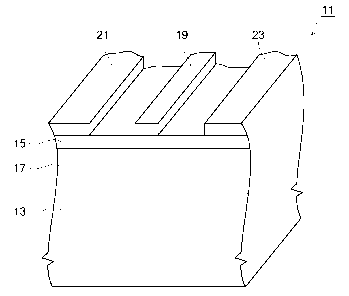
[0022] Fig. 1 is a view representing the high electron mobility transistor
involving Embodiment Mode 1.
Fig. 2A is a view representing the structure of the high electron
mobility transistor (HEMT) in Embodiment Example.
Fig. 2B is a view representing the structure of the HEMT in
Experiment.
Fig. 3 is a view representing a spectrum for (0002) plane XRD in the
surfaces of the AlGaN layers of the epitaxial substrate (sample E~ and the
CA 02564424 2006-10-26
7
epitaxial substrate (sample B) manufactured for the high electron mobility
transistors.
Fig. 4 is a view representing correspondences between leakage current
density and the full width at half maximum for (0002) plane XR,D
characteristic
in the gallium nitride layer.
Fig. 5A is a view representing the manufacture of the epitaxial
substrate involving Embodiment Mode 2.
Fig. 5B is a view representing the manufacture of the epitaxial
substrate involving Embodiment Mode 2.
Fig. 5C is a view representing the manufacture of the epitaxial
substrate involving Embodiment Mode 2.
Fig. 6 is a view representing one example of locations of the high
dislocation regions and the low dislocation regions in the gallium nitride
freestanding substrate for Embodiment Modes 1 and 2.
Fig. 7 is a view representing another example of locations of the high
dislocation areas and the low dislocation areas in the gallium nitride
freestanding substrate for Embodiment Modes 1 and 2.
Fig. 8 is a view representing the high electron mobility transistor
according to one modification of Embodiment Mode 1.
Fig. 9 is a view representing the high electron mobility transistor
according to other modification of Embodiment Mode 1.
Fig. 10 is a view representing the high electron mobility transistor
according to other modification of Embodiment Mode 1.
CA 02564424 2006-10-26
8
Fig. 11 is a view representing the high electron mobility transistor
according to other modification of Embodiment Mode 1.
Explanation ofReferenced Numerals
[0023] 11, 11a, 11b, 11c, 11d: high electron mobility transistor 13:
supporting
substrate 14: additional gallium nitride semiconductor layer 15: AlyGai-yN
epitaxial layer (0< y _<1)~ 16: contact layer 17: GaN epitaxial layer 19, 19a:
Schottky electrode 21, 21a, 21b: source electrode 23, 23a, 23b: drain
electrode
31: gallium nitride substrate 33: gallium nitride film 35: AIGaN film A:
epitaxial substrate 37a: source electrode 37b: drain electrode 39: gate
electrode 41: sapphire substrate 42: seed layer 43: gallium nitride film 45:
AlGaN film B: epitaxial substrate 47a: source electrode 47b: drain electrode
49: gate electrode 80: reactor 83: gallium nitride freestanding substrate 85:
GaN epitaxial film 87: AlGaN epitaxial film 81: epitaxial substrate 82:
gallium nitride freestanding substrate 82c: high dislocation region 82d: low
dislocation region 84: gallium nitride supporting substrate 84c: high
dislocation region 84d: low dislocation region.
Best Mode for Carrying Out the Invention
[0024] Insights into the present invention will be readily understood in
conjunction with the following detailed description with reference to the
accompanying figures for illustration. Hereinafter, referring to the
accompanying figures, embodiments according to Group III nitride
semiconductor devices and epitaxial substrates of the present invention will
be
described. In the embodiments, high electron mobility transistors as a Group
III
CA 02564424 2006-10-26
nitride semiconductor device will be described. Note that where possible
identical components are labeled with the same reference marks.
[0025] Embodiment Mode 1
Fig. 1 is a view representing a high electron mobility transistor
involving Embodiment Mode 1. The high electron mobility transistor 11 is
furnished with a supporting substrate 13, an AlyGai-yN epitaxial layer (0<
y<_1)
15, a GaN epitaxial layer 17, a Schottky electrode 19, a source electrode 21,
and
a drain electrode 23. The supporting substrate 13 is composed of AIRGai-~N (0<
x <1), more specifically, A1N, AlGaN, or GaN. The AlyGai-yN epitaxial layer 15
has a full-width-at-half maximum for (0002) plane XRD of 150 sec or less. The
GaN epitaxial layer 17 is provided between the gallium nitride supporting
substrate 13 and the Als,Gai-yN epitaxial layer 15. The Schottky electrode 19
is
provided on the AlyGai-yN epitaxial layer 15. The source electrode 21 and the
drain electrode 23 are provided on the GaN epitaxial layer 17. As one example
of the present embodiment, the source electrode 21 may be provided on the
AlyGai yN epitaxial layer 15. Moreover, the drain electrode 23 may be provided
on the AI3,Gat-yN epitaxial layer 15. In this example, the source electrode 21
is
in contact with the AIyGaI-yN epitaxial layer 15, and the drain electrode 23
is in
contact with the AlyGal-yN epitaxial layer 15. The Schottky electrode 19
constitutes a gate electrode of the high electron mobility transistor 11.
[0026] According to the inventors' experiments, it has been found that the
leakage current from the Schottky electrode 19 in contact with the AlyGai-yN
epitaxial layer 15 is related to the full-width-at-half maximum for (0002)
plane
CA 02564424 2006-10-26
XRD. Since the full-width-at-half maximum for (0002) plane XRD is 150 sec or
less, the leakage current from the Schottky electrode 19 can reduced.
[0027] Fig. 2A is a view representing structures of a high electron mobility
transistor (HEMT) involving Embodiment Example. Fig. 2B is a view
5 representing structures of an HEMT involving Experiment.
Embodiment Example 1
[0028] A gallium nitride substrate 31 is placed in a reactor of an MOVPE
device. Supplying gases including hydrogen, nitrogen, and ammonia into the
reactor, the gallium nitride substrate 31 undergoes a heat treatment at 1100
10 degrees Celsius for 20 minutes. Next, the temperature of the gallium
nitride
substrate 31 is increased to 1130 degrees Celsius. Ammonia and
trimethylgallium (TMG) are supplied to the reactor to grow a gallium nitride
film 33 having a thickness of 1.5 arm on the gallium nitride substrate 31.
Trimethyl aluminum (TMA), TMG, and ammonia are supplied into the reactor
to grow an AlGaN film 35 of 30 nm on the gallium nitride film 33. By these
processes, an epitaxial substrate A is manufactured. A source electrode 37a
and
a drain electrode 37b of Ti/Al/Ti/Au are formed on a surface of the epitaxial
substrate A, and a gate electrode 39 of Au/Ni is formed on the surface of the
epitaxial substrate A. By these processes, an HEMT-A shown in Fig. 2A is
manufactured.
Experiment 1
[0029] A sapphire substrate 41 is placed in a reactor of the MOVPE device.
Supplying the gases including hydrogen, nitrogen, and ammonia into the
CA 02564424 2006-10-26
11
reactor, the sapphire substrate 41 undergoes a heat treatment at a temperature
of 1170 degrees Celsius for 10 minutes. Next, a seed layer 42 is grown on the
sapphire substrate 41. After this, as in Embodiment Example, a gallium nitride
film 43 and an AlGaN film 45 are grown to manufacture an epitaxial substrate
B. A source electrode 47a and a drain electrode 47b of Ti/Al/Ti/Au are formed
on
the surface of the epitaxial substrate B, and a gate electrode 49 of Au/Ni is
formed on the surface of the epitaxial substrate B. By these processes, an
HEMT-B shown in Fig. 2B is manufactured.
[0030] Fig. 3 is a view representing a spectrum for (0002) plane XRD in the
surfaces of the AlGaN layers of the epitaxial substrate (sample A) and the
epitaxial substrate (sample B) manufactured for the high electron mobility
transistors. The sample A includes a GaN film and an AIGaN film formed on the
gallium nitride substrate in this order. The sample B includes a seed film, a
GaN film and an AlGaN film formed on the sapphire substrate in this order. On
each of the AIGaN films, a Schottky electrode is provided to measure the
leakage current. The Schottky electrode has an area of 7.85x 10⁻⁵ cm2, and the
applied voltage is -5 volts, for example.
Sample A-
FWHM of XRD: 22.4 (sec),
Leakage current density: 1.75x10⁻⁶ (A/cm2)~
Sample B -
FWHM of XRD: 214.4 (sec),
Leakage current density: 1.79U xlp-2 (A/cm2).
CA 02564424 2006-10-26
12
The leakage current in the sample A is largely reduced compared to
the leakage current in the sample B. The reason is that as far as XRD of the
AlGaN layer is concerned, FWHM of the sample A is more acute than that of the
sample B.
[0031) The XRD in the (0002) plane has a wider full-width-at-half maximum
as the number of the screw dislocations included in the AIGaN layer is larger.
Therefore, by making the full-width-at-half maximum small, the leakage
current from the Schottky electrode can be reduced. The forward current
through the gate electrode of the HEMT is about 0.1 A/crri 2, therefore, it is
necessary to limit the leakage current to 1X10⁻⁴ A/cm2, 1/1000 of the forward
current or less. As shown in Fig. 4, since the AlyGai-yN epitaxial layer has a
full-width-at-half maximum for (0002) plane XRD of 150 sec or less, the
leakage
current can be 1X10⁻⁴ A/cm2 or less. Although it is principally possible to
evaluate the crystal quality of the AIGaN layer with XRDs of (0004) plane or
(0006) plane, other than (0002) plane, (0002) plane is preferable for
evaluating
the crystal quality of the AlGaN layer because (0002) plane has the great XRD
strength.
[0032] Fig. 4 is a view representing correspondences between leakage current
density and the full-width-at-half maximum for (0002) plane XRD
characteristic in the gallium nitride layer. Symbols indicated by reference
marks 51a through 51h represent values obtained by measuring structures in
which Schottky electrodes are manufactured on the AIGaN layer fabricated by
utilizing the gallium nitride substrate. Symbols indicated by reference marks
CA 02564424 2006-10-26
13
53a through 53f represent values obtained by measuring structures in which
Schottky electrodes are formed on the AlGaN layers fabricated by utilizing the
sapphire substrates.
Embodiment Example 2
[0033] To present specific examples
Sample indicated by the reference mark 51a-
Full-width-at-half maximum= 22.4 sec,
Leakage current density: 1.75X10-sA/cm2~
Sample indicated by the reference mark 51b-
Full-width-at-half maximum= 70.3 sec,
Leakage current density= 4.37X 10⁻⁵ A/cm2
Sample indicated by the reference mark 51c-
Full-width-at-half maximum= 70.3 sec,
Leakage current density 1.11X10⁻⁵A/cm2~
Sample indicated by the reference mark 51d-
Full-width-at-half maximum: 70.9 sec,
Leakage current density 9.01X10-~ A/cm2
Sample indicated by the reference mark 51e-
Full-width-at-half maximum: 70.9 sec,
Leakage current density: 2.72X10-gA/cm2~
Sample indicated by the reference mark 51f
Full-width-at-half maximum: 110.1 sec,
Leakage current density: 2.45X 10-s A/cm2
CA 02564424 2006-10-26
14
Sample indicated by the reference mark 51g-
Full-width-at-half maximum: 124.8 sec,
Leakage current density: 3.05x10⁻⁵ A/cm2
Sample indicated by the reference mark 51h-
Full-width-at-half maximum: 141.3 sec,
Leakage current density: 9.70X 10⁻⁶ A/cm2.
Experiment 2
[0034] To present a specific example:
Schottky diode structure of the reference mark 53a (with the smallest
full-width-at-half maximum and leakage current density)-
Full-width-at-half maximum: 182.6 sec,
Leakage current density: 2.15X10⁻³ A/cm2.
[0035] In the high electron mobility transistor 11, a supporting substrate 13
of nitride is composed of gallium nitride conductive or semi-insulating. In
this
example, the gallium nitride region is homoepitaxially grown on the gallium
nitride supporting substrate. The gallium nitride supporting substrate has a
carrier concentration of 1X1019 cm 3 or less. The GaN layer 17 has a thickness
between 0.1 arm and 1000 Vim, inclusive. The GaN layer 17 has a carrier
concentration of 1X101 cm 3 or less. The AIGaN layer 15 has a thickness
between 5 nm and 50 nm, inclusive. The AlGaN layer 15 has a carrier
concentration of 1X1019 cm 3 or less.
[0036] In the high electron mobility transistor 11, aluminum composition Y of
the Alf.Gal-yN epitaxial layer 15 is preferably 0.1 or more. If the aluminum
CA 02564424 2006-10-26
composition Y is less than 0.1, the band offset becomes small so that
two-dimensional electron gas having enough density can not be formed at the
AlGaN/GaN interface. Furthermore, the aluminum composition Y is preferably
0.7 or less. If the aluminum composition Y is more than 0.7, it is highly
likely
5 that cracks are generated in the AlGaN layer. The generation of the cracks
prevents the two-dimensional electron gas from being formed at the
AlGaN/GaN interface.
(0037] In the high electron mobility transistor 11, the AlyGal-yN epitaxial
layer 15 preferably has a thickness of 5 nm or more. If the thickness of the
10 Alf.Gai-yN epitaxial layer 15 is less than 5 nm, the distortion at the
AlGaN/GaN
interface becomes small and the two-dimensional electron gas is not formed.
Furthermore, the AlyGai-yN epitaxial layer 15 preferably has a thickness of 50
nm or less. If the thickness of the AlyGal-yN epitaxial layer is more than 50
nm,
it is highly likely that the cracks are generated in the AlGaN layer. The
15 generation of cracks prevents the two-dimensional electron gas from being
formed at the AlGaN/GaN interface.
(0038] The AlxGai-xN supporting substrate for the high electron mobility
transistor 11 is preferably composed of gallium nitride. Accordingly, Group
III
nitride semiconductor devices are provided using a supporting substrate of a
low dislocation density.
[0039] Embodiment Mode 2
Fig. 5A, Fig. 5B, and Fig. 5C are views representing manufacture of
the epitaxial substrate according to Embodiment Mode 2. As shown in Fig. 5A, a
CA 02564424 2006-10-26
16
gallium nitride freestanding substrate 83 having conductivity is placed in a
reactor 80. The following crystal growth is preferably performed by MOVPE
method. The gallium nitride freestanding substrate 83 has a carrier
concentration of 1X1019 cm-3 or less. As shown in Fig. 5B, by supplying TMG
and NHa, a GaN epitaxial film 85 is deposited on a first surface 83a of the
gallium nitride freestanding substrate 83. The GaN epitaxial film 85 is
preferably undoped. The GaN epitaxial film 85 is deposited at a temperature
between 600 degrees Celsius and 1200 degrees Celsius, inclusive. The pressure
in the reactor is between 1 kPa and 120 kPa, inclusive. The gallium nitride
epitaxial film 85 has a thickness between 0.5 7rm and 1000 arm, inclusive. The
GaN epitaxial film 85 has a carrier concentration of 1X101 cm-3 or less. If
necessary, in advance of the growth of the GaN epitaxial film 85, a buffer
layer
can be grown. The buffer layer may be composed of any of A1N, GaN, AlGaN,
InGaN, and AIInGaN. The buffer layer restrains defects or impurities of the
gallium nitride freestanding substrate 83 from affecting the GaN epitaxial
layer 85, so that quality of the GaN epitaxial layer 85 can be improved.
Next, as shown in Fig. 5C, TMA, TMG and NH3 are supplied to deposit
an undoped or n-type AIGaN epitaxial film 87 onto the undoped GaN epitaxial
film 85. The AlGaN epitaxial film 87 is deposited at a temperature between 600
degrees Celsius and 1200 degrees Celsius, inclusive. The pressure in the
reactor
is between 1 kPa and 120 kPa, inclusive. The aluminum composition of the
AIGaN epitaxial film 87 is between 0.1 and 0.7, inclusive. The AlGaN epitaxial
film 87 has a thickness of 5 nm and 50 nm, inclusive. The AIGaN epitaxial film
CA 02564424 2006-10-26
17
87 has a carrier concentration of 1X1019 cm~3 or less. Accordingly, an
epitaxial
substrate 81 is obtained. By making use of this substrate, an HEMT according
to Embodiment Mode 1 can be manufactured.
[0040] The inventors have found that the leakage current from the Schottky
electrode in contact with the AlyGai-yN epitaxial film 87 (0< y __<1) is
related to
the full-width-at-half maximum for (0002) plane XRD. In the epitaxial
substrate, the leakage current from the Schottky electrode formed on the
Alf,Gai-yN epitaxial is small. Accordingly, an epitaxial substrate preferable
for
the high electron mobility transistor can be provided, for example.
Especially, if
the full-width-at-half maximum for (0002) plane XRD is 150 sec or less, as
apparent from Fig. 4, it is possible to reduce the leakage current from the
Schottky electrode compared to a case of 150 sec or more.
[0041] On a surface of the AlGaN epitaxial film 87 of the epitaxial substrate
81, a Schottky electrode film for a gate electrode and ohmic electrode films
for a
source electrode and a drain electrode are deposited. The Schottky electrode
and the ohmic electrode are formed from the Schottky electrode film and the
ohmic electrode film, respectively. After thinning a portion of the AlGaN
epitaxial film 8? immediately under the Schottky electrode, a Schottky
electrode may be formed on the portion. Accordingly, it is possible to reduce
the
source resistance, improve the mutual conductance, and perform normally off:
Furthermore, by adding n-type dopant, an n-type semiconductor region may be
formed immediately under the source electrode and/or the drain electrode.
Furthermore, n-type semiconductor regions to which n-type dopant is added
CA 02564424 2006-10-26
18
may be grown as contact layers on the surface of the AlGaN epitaxial film 87,
and on the contact layers a source electrode and/or a drain electrode may be
formed. Accordingly, the contact resistance can be reduced. Furthermore, after
thinning a portion of the AIGaN layer, a source and/or a drain electrode may
be
formed on the portion. Accordingly, the contact resistance can be reduced.
Alternatively, the source and/or drain electrode may be formed to be in
contact
with the GaN layer having a band gap smaller than that of AlGaN by removing
the AlGaN layer. Accordingly, the contact resistance can be reduced. Since the
full-width-at-half maximum for (0002) plane XRD in the AlGaN region is used
as an indicator of the crystal quality to monitor the quality of the AIGaN
film
with which the Schottky electrode constitutes a Schottky junction, an
epitaxial
substrate can be provided for semiconductor devices in which the backward
leak current flowing through the Schottky junction when a voltage is applied
across the Schottky electrode and the ohmic electrode can be reduced.
[0042) Fig. 6 is a view representing one example of locations of high
dislocation regions and low dislocation regions in a gallium nitride
freestanding
substrate for Embodiment Modes 1 and 2. A first surface 82a of the gallium
nitride freestanding substrate 82 for the epitaxial substrate 81 includes
first
areas where high dislocation regions 82c having a relatively large screw
dislocation density appear, and a second area where a low dislocation region
82d having a relatively small screw dislocation density appears. The high
dislocation regions 82c are surrounded by the low dislocation region 82d, and
the first areas are randomly distributed in a dot-like pattern in the second
area
CA 02564424 2006-10-26
19
on the first surface 82a. As a whole, the screw dislocation density is 1X 10⁸
cm-2
or less, for example. The epitaxial substrate 81 gives an epitaxial layer
having a
lowered dislocation density in the low dislocation region 82d. Consequently,
the
backward leak current is reduced and the backward breakdown voltage is
improved.
(0043] Fig. 7 is a view representing another example of locations of the high
dislocation regions and the low dislocation regions in a gallium nitride
freestanding substrate for Embodiment Modes 1 and 2. A first surface 84a of
the
gallium nitride freestanding substrate 84 for the epitaxial substrate 81
includes
first areas where high dislocation regions 84c having a relatively large screw
dislocation density appear, and second areas where low dislocation regions 84d
having a relatively small screw dislocation density appear. The high
dislocation
regions 84c are surrounded by the low dislocation regions 84d, and the first
areas are distributed in a striped pattern in the second area on the first
surface
84a. As a whole, the screw dislocation density is 1X108 cm 2 or less, for
example.
The epitaxial substrate 81 gives an epitaxial layer having a lowered
dislocation
density in the low dislocation regions 84d. Accordingly, the backward leak
current is decreased, and the backward breakdown voltage is improved.
[0044] In the present embodiment, as in Embodiment Mode 1, as a
freestanding substrate, the Al~Gai-~N (0< x < x <1) substrate can be used.
More
specifically, the freestanding substrate can be composed ofAlN, AlGaN or GaN.
[0045] Fig. 8 is a view representing the high electron mobility transistor
according to one modification of Embodiment Mode 1. Referring to Fig. 8, the
CA 02564424 2006-10-26
high electron mobility transistor 11a can be provided with an additional
gallium
nitride semiconductor layer 14 between the GaN epitaxial layer 17 and the
gallium nitride supporting substrate 13. The gallium nitride semiconductor
layer 14 is composed of A1N, GaN, AlGaN, InGaN, or AlInGaN, for example.
5 The gallium nitride semiconductor layer 14 restrains the affects of defects
of
and impurities on the supporting substrate from propagating to upper layers,
thereby improving the quality of the GaN epitaxial layer 17.
[0046) Fig. 9 is a view representing the high electron mobility transistor
according to other modification of Embodiment Mode 1. The high electron
10 mobility transistor 11b can be provided with an AlGaN layer 15a, in place
of the
AlGaN layer 15 of the high electron mobility transistor 11a. The AlGaN layer
15a includes a first portion 15b, a second portion 15c, and a third portion
15d.
The first portion 15b is positioned between the second portion 15c and the
third
portion 15d. The thickness of the first portion 15b is smaller than that of
the
15 second portion 15c and that of the third portion 15d, thereby forming a
recess
structure in the AlGaN layer 15a. On the first portion 15b, a gate electrode
19a
is provided. The recess structure is formed by thinning the Als.Gai-YN
epitaxial
layer 15 by etching, for example. The recess gate structure makes it possible
to
reduce the source resistance, improve the mutual conductance, and perform the
20 normally off.
[0047) Fig. 10 is a view representing the high electron mobility transistor
according to other modification of Embodiment Mode 1. The high electron
mobility transistor llc may be provided with an AlGaN layer 15e, in place of
the
CA 02564424 2006-10-26
21
AlGaN layer 15 of the high electron mobility transistor 11a. The AlGaN layer
15e includes a first portion 15f, a second portion 15g, and a third portion
15h.
The first portion 15f is positioned between the second portion 15g and the
third
portion 15h. The thickness of the first portion 15f is larger than that of the
second portion 15g and that of the third portion 15h, thereby forming a recess
structure in the AlGaN layer 15e. The recess structure can be formed by
thinning the AlyGai-yN epitaxial layer 15 by etching, for example. The source
electrode 21a is provided on the second portion 15g, and the source electrode
23a is provided on the third portion 15h. This recess ohmic structure can
reduce
the contact resistance.
[0048] Fig. 11 is a view representing the high electron mobility transistor
according to other modification of Embodiment Mode 1. The high electron
mobility transistor lld can be furtherer provided with contact layers 16 for a
source electrode and a drain electrode. The contact layers 16 are provided on
the AlGaN layer 15 of the high electron mobility transistor 11a. The contact
layers 16 may be composed of gallium nitride semiconductors such as GaN,
InN, and InGaN. The band gap of the contact layer 16 is preferably smaller
than that of the AlGaN layer 15. In addition, the carrier concentration of the
contact layer 16 is preferably larger than that of the AIGaN layer 15. The
gate
electrode 19 constitutes a Schottky junction with the AlGaN layer 15, and the
source electrode 21b and the drain electrode 23b constitute ohmic contacts
with
the contact layer. The contact layer added structure can reduce the contact
resistance.
CA 02564424 2006-10-26
22
[0049 In the preferable embodiments, principles of the present invention
were described with illustrations, but it will be recognized by persons
skilled in
the art that the present invention can be changed in locations and in detail
without departing from the principles. The present invention is not limited to
the specific configurations disclosed in the present embodiments. Accordingly,
the rights in the scope of the patent claims, and in all modifications and
changes deriving from the scope of the spirit thereof are claimed.