Note: Descriptions are shown in the official language in which they were submitted.
CA 02566476 2006-11-09
WO 2005/112281 PCT/CA2005/000732
ET D AND YSTEM F SPURIOUS SIGNAL CONTR L 1N R E VER
FIELD OF THE INVENTION
[0001] The present invention relates generally to communications, and to down
conversion of an RF signal to a lower frequency in a radio. More specifically,
the present
invention relates to management of spurious components generated by the radio.
BACKGROUND OF THE INVENTION
[00021 Many communication systems up-convert electromagnetic signals from base
band to higher frequencies for transmission, and subsequently down-convert
those high
frequencies back to their original frequency band when they reach the
receiver, processes
known as up-conversion and down-conversion (or modulation and demodulation)
respectively. The original (or base band) signal, may be, for example, data,
voice or video.
These base band signals may be produced by transducers such as microphones or
video
cameras, be computer generated, or transferred from an electronic storage
device. In
general, the high frequencies provide longer range and higher capacity
channels than base
band signals, and because high frequency radio frequency (RF} signals can
propagate
through the air, they can be used far wireless transmissions as well as hard-
wired or fibre
channels.
[0003] All of these signals are generally referred to as radio frequency (RF}
signals,
which are electromagnetic signals; that is, waveforms with electrical and
magnetic properties
within the electromagnetic spectrum normally associated with radio wave
propagation.
[0004] A typical artefact resulting from the down-conversion process are
blocking
signals, also termed spurious components, generated by the radio which can
desensitize the
receiver. These blocking signals appear at an unwanted radio frequency, and
can
desensitize the receiver by raising the noise floor, causing a reduction in
the overall gain of
the receiver, or a combination of both.
[0005] Many different receiver architectures have been proposed and used for
mitigating the effect of blocking signals. These include super-heterodyne,
image rejection,
direct conversion, near zero-1F conversion and harmonic mixing architectures.
A brief
summary of these architectures follows.
CA 02566476 2006-11-09
WO 2005/112281 PCT/CA2005/000732
[0006] The super-heterodyne receiver uses a two-step frequency translation
method
to convert the signal at RF to a base band signal. First, the incoming signals
and corruptive
noise are passed through a band pass filter that attenuates out of band
signals and passes
the desired signal. At this stage some of the blocking signals that are out of
band are
filtered. The desired signal, plus residual blocking signals, are amplified
and mixed with a
first local oscillator. This causes both a down-conversion and an up-
conversion in the
frequency domain. Usually the down-converted portion is retained at the so-
called
"Intermediate Frequency" (IF). Further filtering is performed on the signal at
the iF frequency
using a discrete device. This filter is a band pass filter and retains the
radio channel required
and further reduces the residual blocking signal. The signal is then mixed
with a second
oscillator that causes frequency translation to base band. The disadvantages
of the super
heterodyne architecture include the requirement for an expensive off chip IF
filter, a
frequency plan fixed in hardware, and locations of spurious signals that are
fixed relative to
the RF wanted signal in hardware, meaning that they cannot be changed using a
software
change.
[0007] There are several image rejection architectures that have been
proposed, and
among these, the two most well known are the Hartley Image Rejection
Architecture and the
Weaver Image Rejection Architecture., Here a spurious signal is created and is
located. at a
fixed location in frequency relative to frequency of the wanted signal. This
spurious signal is
commonly referred to as the imagining frequency. The imagining blocking signal
is removed
using a combination of phase shifters and adders that are applied directly to
the radio signal
itself or/and the local oscillator (LO) signal. Some methods employ poly-phase
filfiers to
cancel the image components. Generally, either accurate phase shifters or
accurate
generation of a quadrature-mixing signal are employed in these architectures
to cancel the
image frequency. The amount of image (or blocker) cancellation is directly
dependent upon
the degree of accuracy in producing the phase shift or in producing the
quadrature mixing
signals. Although the integratability of these architectures is high, their
performance is
relatively poor due to the required accuracy of the phase shifts and
quadrature oscillators.
Another disadvantage here is the location of the blocker signal (or image
frequency) is fixed
relative to the wanted signal and cannot be moved to another location.
_2_
CA 02566476 2006-11-09
WO 2005/112281 PCT/CA2005/000732
[0008] Direct conversion architectures perForm the RF to base band frequency
translation in a single step. The RF signal is mixed with a local oscillator
at the carrier
frequency. There is therefore no image frequency, and no image components to
corrupt the
signal. Direct conversion receivers offer high integration, but also have
several important
problems. Classical direct conversion receivers have thus far proved useful
only for
signalling formats that do not place appreciable signal energy near DC after
conversion to
base band. Though direct conversion does not suffer from blocking signals in
general, there
are several typical problems found in integrated direct conversion receivers.
The noise near
base band (i.e. 1/f noise) corrupts the desired signal, the local oscillator
leaks, which creates
DC offsets and causes desensitization, noise inherent to mixed-signal
integrated circuits
corrupts the desired signal, and large on-chip capacitors are required to
remove unwanted
noise and signal energy near DC.
[0009] The near zero-IF conversion architecture is similar to the direct
conversion
architecture, in that the RF band is brought close to base band in a single
step. The desired
signal is not brought exactly to base-band however, and therefore DC offsets
and 1/f noise
do not contaminate the signal. Image frequencies (i.e. the blocker) are again
a problem as in
the super-heterodyne and image rejection architectures. Specific problems
encountered with
these architectures include a second down conversion being performed in the
digital domain
due to spurious issues, a fixed frequency of the image based on the frequency
planning
which cannot be changed, the need for several balanced signal paths for image
cancellation,
corruption of the desired signal due to noise inherent to mixed-signal
integrated circuits, and
the filters used to finer the IF signal inherently contributes to the
frequency planning, making
them standard specific.
[0010] The harmonic mixing architecture uses a number of mixing signals that
are
phase shifted by some desired amount. If x(t) is the incoming RF signal, and
a,, a2, and a3
are the mixing signals, the output of a harmonic mixing structure equals
x(t)*(al+a2+a3). In
this example, there are assumed to be three mixing signals. Here, a,, a2, and
a3 are
constructed so that when they add they have significant energy at the wanted
carrier
frequency. The frequency of al, a2, and a3 are usually the same. In all cases,
al+a2+a3 will
have other frequency components other than the wanted carrier frequency. This
produces a
_3_
CA 02566476 2006-11-09
WO 2005/112281 PCT/CA2005/000732
fixed spurious response. The disadvantage here is the spurious components are
fixed based
on the frequency planning of the additive signals (for example al, a2, and
a3).
(0011] The virtual local oscillator (VLO) receiver architecture described in
commonly
owned U.S. Patent No. 6,727,764, the contents of which are incorporated herein
by
reference, is directed to the generation of signals used in the conversion
process. The virtual
local oscillator receiver architecture has properties that overcome the image-
rejection
problems associated with heterodyne receivers and transmitters, and the LO-
leakage and 1/f
noise problems associated with direct conversion receivers and transmitters.
Figure 1
generally illustrates the main concepts of the virtual local oscillator
receiver architecture.
[0012] The VLO receiver 10 essentially consists of two mixers 12 and 14 that
are
connected together. Other parts of the receiver are not shown to simplify the
schematic. At
the LO ports of the mixers 12 and 14 the signals ~~ and ~2 are applied such
that the overall
RF signal x(t) is multiplied by a signal having significant power at the RF
carrier frequency.
Figure 2 illustrates example ~~ and ~2 waveforms that can be applied to VLO
receiver 10, and
~ the resulting base band output signal Jeff , which represents the actual
desired local oscillator
frequency. The resulting base band output signal Jeff = ~~*~~ has significant
power at the RF
frequency, but in practice there will be power generated in places other than
the RF carrier
frequency.
(0013] This power is denoted as unwanted power, the amount which is determined
by the timing delay and frequency of signal ~~. Figure 3 shows a possible
~~*~2 spectrum
where the desired signal at c~,~ has good power, but due to timing delay of
~2, additional tones
will appear and are placed at harmonics of ~2 away from wrf . In the present
example, the
tones appear at wrf + 200MHz and wrf -200MHz. Unfortunately, this unwanted
power will
down convert signals located at the unwanted power frequencies. For example,
if there is
unwanted power at w,~ + 200MHz in ~~*~z and there is an out off band blocker
signal 20 at ~rf
+ 200MHz as shown in Figure 4, this blocker 20 will eventually be down
converted on top of
the desired signal 22 if left uncorrected, as shown in Figure 5. Since the two
signals overlap,
filtering will be ineffective for removing the blocker signal 20.
(0014] Accordingly, the VLO receiver receiving such an overlapping signal will
drop
the transmission since the overlapping signals will result in corrupted data
that cannot be
properly processed or simply resolved by the receiver.
-4-
CA 02566476 2006-11-09
WO 2005/112281 PCT/CA2005/000732
[0015] It is, therefore, desirable to provide a method and system for reducing
or
eliminating blocker signals from an RF input signal that can desensitize a VLO
receiver and
potentially cause loss of received data.
SUMMARY OF THE INVENTION
[0016] If is an object of the present invention to obviate or mitigate at
least one
disadvantage of the previous blocker signal mitigation schemes. More
specifically, it is an
object of the present invention to modify the spurious profile by adjusting
one of the mixer
signals of the mixer signals used to generate an effective local oscillator
signal used in a
virtual local oscillator receiver. This results in an unwanted RF tone that
does not overlap
with a wanted signal at the desired frequency.
[0017] In a first aspect, the present invention provides a blocking signal
reduction
system for a virtual local oscillator receiver receiving an RF input signal
and providing a
corresponding base band signal. The system includes a synthesizer circuit,
evaluation
means and a dynamic correction circuit. The synthesizer circuit generates a
first mixer signal
and a second mixer signal. The virtual local oscillator receiver receives the
first mixer signal
and the second mixer signal for down converting the RF input signal to an
effective local
oscillator frequency, the down converted RF input signal being provided as the
corresponding base band signal. The evaluation means receives the RF input
signal and
generates an enable signal when the RF input signal is determined to be
deficient. The
dynamic correction circuit senses a power of the base band signal, and
provides a new
frequency value in response to the enable signal, the synthesizer circuit
adjusting a
frequency of the second mixer signal to correspond with the new frequency
value.
(0018] According to embodiments of the present aspect, the evaluation means
can
include base band processor circuits executing pre-set RF input signal status
algorithms, or
the evaluation means can include a blocker detection circuit coupled to the
virtual local
oscillator receiver for sensing a characteristic corresponding to the RF input
signal, the
blocker detection circuit generating the enable signal in response to the
sensed characteristic
exceeding a predetermined threshold.
-5-
CA 02566476 2006-11-09
WO 2005/112281 PCT/CA2005/000732
[0019] In aspects of the present embodiment, the RF input signal can include
RF
input frames, and the corresponding base band signal can include base band
frames. The
dynamic correction circuit can include a power detector circuit, a comparator
circuit, and a
memory. The power detector circuit receives and senses the power of a first
base band
frame and the power of a second base band frame in response to the enable
signal. The
comparafior circuit compares the power of the second base band frame to the
power of the
first base band frame, the comparator circuit generating a memory access
signal when the
power of the first base band frame is less than or equal to the power of the
second base
band frame. The memory stores a plurality of new frequency values, and
provides one of
said new frequency values to the synthesizer circuit in response to the memory
access
signal. The dynamic correction circuit can include a timer for controlling the
power detector
circuit to measure the power of the second base band frame at a set time after
the power of
the first base band frame is measured. The dynamic correction circuit can
include a counter
responsive to the memory access signal for providing each of the new frequency
values.
[0020] In yet another aspect of the present embodiment, the blocker detection
circuit
can include a power sensing circuit, and the characteristic can include a
signal power level of
the RF input signal. in another aspect of the present invention, the virtual
local oscillator
receiver can include a variable gain amplifier and an automatic gain control
circuit. The
variable gain amplifier provides the base band signal. The variable gain
amplifier receives a
control voltage for maintaining gain of the base band signal at a
predetermined value. The
automatic gain control circuit receives the base band signal for generating
the control
voltage. The blocker detection circuit can include a gain comparison circuit
for measuring a
difference in gain between a first base band frame and a second base band
frame, the gain
comparison circuit generating the enable signal when the difference in gain
exceeds the
predetermined threshold.
[0021] In a second aspect, the present invention provides a blocking signal
reduction
system for a virtual local oscillator receiver receiving an RF input signal
and providing a
corresponding base band signal. The system includes a synthesizer circuit, a
memory, and
configuration logic. The synthesizer circuit generates a first mixer signal
and a second mixer
signal. The virtual local oscillator receiver receives the first mixer signal
and the second
mixer signal for down converting the RF input signal to an effective local
oscillator frequency,
_g_
CA 02566476 2006-11-09
WO 2005/112281 PCT/CA2005/000732
the down converted RF input signal being provided as the corresponding base
band signal.
The memory stores preselected frequency values corresponding to specific
channels and
standards, the memory providing one of said stored preselected frequency
values to the
synthesizer circuit in response to an addressing signal. The configuration
logic receives
information corresponding to a standard and channel, the configuration logic
generating the
addressing signal in response to the standard and channel information. The
synthesizer
circuit adjusts a frequency of the second mixer signal to correspond with the
one of said
stored preselected frequency values.
[0022] In a third aspect, the present invention provides a method for
eliminating a
blocking signal in an RF input signal received by a virtual local oscillator
receiver, the virtual
local osciNatar receiver receiving a first mixer signal and a second mixer
signal for generating
a corresponding base band signal. The method includes a) detecting the
presence of the
blocking signal in the RF input signal; b) changing a value of the second
mixer signal; c)
sensing a power of the corresponding base band signal; and d) repeating steps
b) and c)
until a preset condition is satisfied.
[0023] In embodiments of the present aspect, the RF input signal can include
RF
input frames, and the corresponding base band signal can include base band
frames. The
step of detecting can include measuring a power of the RF input signal and
comparing the
measured power to a predetermined threshold. In another embodiment, the step
of detecting
can include comparing a drop in gain of the base band signal to a
predetermined value, and
the step of detecting can include comparing the gain of a first base band
frame to the gain of
a second base band frame.
(0024] According to further embodiments of the present aspect, the step of
sensing
can include sensing a power of a first base band frame, the step of repeating
can include
sensing a power of a second base band frame and comparing the power of the
second base
band frame to the power of the first base band frame. The preset condition can
be the
second base band frame having a lower power than the first base band frame,
and a table
can store a predetermined number of frequency values. The step of repeating
can include
changing the value of the second mixer signal to correspond with a different
frequency value
stored in the table for each iteration. The preset condition can include
having changed the
value of the second mixer signs( with all the frequency values stored in the
table. A buffer
-7-
CA 02566476 2006-11-09
WO 2005/112281 PCT/CA2005/000732
can be used to store the frequency value of the second mixer signal
corresponding to the
base band frame having the lowest power.
[0025] Other aspects and features of the present invention will become
apparent to
those ordinarily skilled in the art upon review of the following description
of specific
embodiments of the invention in conjunction with the accompanying figures.
BRIEF DESCRIPTION OF THE DRAWINGS
[0026] Embodiments of the present invention will now be described, by way of
example only, with reference to the attached Figures, wherein:
Fig. 1 is a general circuit schematic of a known virtual local oscillator
receiver
1 o circuit;
Fig. 2 is a timing diagram illustrating the virtual local oscillator mixer
waveforms;
Fig. 3 is an approximate power spectrum of ~~*~~ for illustrating the
generation
of unwanted tones due to mixer signal error in the virtual local oscillator
receiver of
Figure 1;
Fig. 4 is a power spectrum plot illustrating corresponding position of a
blocker
signal at the unwanted tone of Figure 3;
Fig. 5 is a power spectrum plot illustrating the result of down conversion of
the
blocker signs( with the desired signal;
Fig. 6 is a power spectrum plot illustrating the effect of adjusting one of
the
mixer signals by a predetermined frequency value, according to an embodiment
of
the present invention;
Fig. 7 is a power spectrum plot illustrating a down-conversion result after
adjusting one of the mixer signals by the predetermined frequency value,
according to
an embodiment of the present invention;
Fig. 8 is a block diagram of a simplified VLO receiver circuit using preset ~2
values to remove spurious signals, according to an embodiment of the present
invention;
Fig. 9 is a flow chart of a method for dynamic spurious correction in a VLO
3o receiver circuit, according to an embodiment of the present invention;
_g_
CA 02566476 2006-11-09
WO 2005/112281 PCT/CA2005/000732
Fig. 70 is a schematic of a VLO receiver with a power sensing enabled
blocking signal reduction system according to an embodiment of the present
invention; and,
Fig. 11 is a schematic of a VLO receiver with a gain difference enabled
blocking signal reduction system according to an embodiment of the present
invention.
DETAILED DESCRIPTION
[0027] Generally, the present invention provides a method and system for
1 o dynamically shifting spurious tones away from the desired frequency in a
virtual local
oscillator receiver, such that any undesired signal residing at such spurious
tones are
effectively delineated from the desired signal and removed from the RF input
signal. The
system detects the presence of potential undesired blocker signals in the RF
input signal,
and initiates an iterative power comparison and mixer signal adjustment loop.
As the virtual
local oscillator uses two mixer signals, the frequency of one of the mixer
signals is adjusted
during the loop until the power of the down-converted signal is minimized to a
predetermined
level. Minimized power in the down-converted signal is indicative of the
absence of the
blocker signal, since the presence of a relatively high power signal is
indicative of a blocker
signal overlapping with a desired signal.
[0028 The embodiments of the present invention take advantage of a property of
virtual local oscillator circuits, such as VLO receiver 10 shown in Figure 1.
In the VLO
receiver 10 shown in Figure 1, the location of the spurious profile of ~z*~Z
in the frequency
domain can be modified by adjusting ~2. The dominate frequency, being the
frequency having
the highest power of ~~*~2 , will be at the RF frequency which is independent
of the frequency
c~2 is set to. Accordingly, by adjusting ~2, the location of the spurious
signal can be shifted as
shown in Figure 6. After down conversion, the spectrum will appear as shown in
Figure 7,
with the unwanted signal 22 being separated from the desired signal 20. With
the two signals
being segregated, a low pass filter function 24 can be applied to filter out
unwanted signal
22.
_g_
CA 02566476 2006-11-09
WO 2005/112281 PCT/CA2005/000732
[0029] Another useful property that the embodiments of the present invention
take
advantage of is the power of the desired signal and the overlapping Mocker
signal. As
previously discussed, unwanted power at the spurious frequency in ~~*~2 will
down convert a
block signal located at the spurious frequency, such that the blocker signal
is down
converted on top of the wanted signal. However, this down converted power of
the unwanted
signal will be attenuated by the difference between the power of the wanted
signal minus the
power of the unwanted Mocker signal, which can be approximately 37dB for
example, If
RFwanted denotes the wanted RF power, and WmU denotes Wanted power minus
Unwanted power, the total amount of power at base band can be expressed as:
[0030] BBpower = RFwanted + 10~(-WmU/10)*RFunwanted
[0031] This combined power typically exceeds expected power of the desired
signal
by an amount of 10"(-WmU/10)*RFunwanted. Therefore, the presence of this
magnitude of
power is indicative of a situation in which an unwanted blocker signal is
overlapping a
desired signal, resulting from ~2 inaccuracy in the VLO receiver. Therefore,
it follows that by
shifting the unwanted blocker signal away from the desired signal in the ~~*~2
frequency
domain, the BBpower will drop by an amount of approximately 10~(-
WmUl10)*RFunwanted.
[0032] Accordingly, the blocker signal overlap with the desired signal can be
eliminated by adjusting the frequency of ~z such that the RFunwanted tone does
not fail on
top of the wanted signal at base band. In addition to adjusting the frequency
of ~2, the time
delay of ~~ can be adjusted to modify the value WmU. In either approach, the
BBpower is
minimized.
(0033] With these properties of the VLO receiver 10, methods for detecting and
correcting for a blocker signal have been developed for VLO receiver 10, or
similar systems
that combine two mixer signals to produce an effective desired local
oscillator signal. Two
schemes can be used for removing a blocking signal from overlapping a desired
signal. The
first is to use preselected ~2 values that are known to remove a blocking
signal based on field
trials or simulations. These values can be stored in memory and selected for a
particular
channel and standard, or a combination of different channels and standards.
The second is
dynamic correction of the spurious profile so that a blocker signal will not
be placed onto the
desired signal in base band.
-10-
CA 02566476 2006-11-09
WO 2005/112281 PCT/CA2005/000732
(0034] The implementation embodiment of the first scheme will be described
with
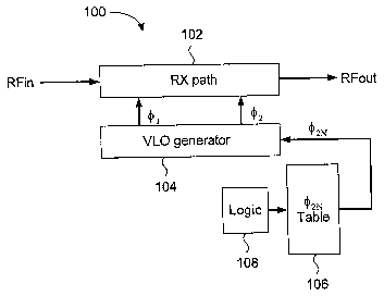
reference to Figure 8. In the simplified VLO receiver system 100 of Figure 8,
a receiver path
102 similar to VLO receiver 10 shown in Figure 1, receives ~~ and ~~ provided
by VLO
generator 104. VLO generator can also be referred to as a synthesizer circuit.
A memory 106
storing the predetermined ~2 values for different channels and different
standards, provides a
selected ~Z value to VLO generator 104. Configuration logic 108 addresses the
appropriate ~Z
value based on the presently used channel and standard. The memory 106 can be
implemented in the radio, in the processor, or in a discrete memory on a
printed circuit board
of the wireless device. The selection of ~z is based on a system understanding
of where
spurious tones can be placed so that they do not significantly degrade the
wanted RF signal.
As an example, ~2 can be selected based on the following criteria: 1 ) No
spurious content is
within the bandwidth of the all the channels; and 2) The first spurious value
is >10MHz from
the edges of the band.
[0035] The corresponding method for operating the simplified VLO receiver
system
100 of Figure 8 is straightforward. The channel/standard logic 108 detects the
standard being
used and the communication channel, and addresses the appropriate ~z value
from memory
106. This selected ~2 value is provided to VLO generator 104, which generates
the new ~2
value. Unfortunately, this scheme would not be effective for standards adopted
after the ~Z
values have been programmed, and the ~Z values are limited by the number of
different test
conditions or simulations that are performed.
[0036] Therefore, the dynamic correction scheme may be the more suitable
method
since it does not require any knowledge of operating standards, or feedback
from
testing/simulation of signals to determine appropriate ~2 values. A method for
dynamic
detection and removal of a blocker signal from an RF input signal will now be
discussed with
reference to Figure 9.
[0037] The method of Figure 9 operates in the wireless communication context,
where data is transmitted in a series of frames, where each frame can be
hundreds of
microseconds in duration and received in succession by a receiver. For
example, the GSM
standard specifies frame durations of 577 microseconds. Once down converted
with the VLO
receiver, each received frame will have an associated base band power which
may include a
blocking signal overlapping the desired signal, as previously noted.
Therefore, according to
-11 -
CA 02566476 2006-11-09
WO 2005/112281 PCT/CA2005/000732
the present embodiment, ~2 can be adjusted for each successive frame until the
base band
power is minimized.
[0033] The method of Figure 9 includes two distinct phases. The first phase
involves
the detection of the presence of an overlapping blocker signal, or some other
suitable trigger,
which will initiate the second phase. While detection of the overlapping
Mocker signal can be
monitored frame to frame, the initiation of the second phase can be automatic
upon power up
reset of the wireless device. Further discussion of blocker signal detection
techniques will be
described later with reference to Figures 10 and 11. The second phase is a ~2
adjustment
loop for shifting the blocker signal away from the desired signal. Generally,
this adjustment
loop will identify the c~2 value yielding the lowest base band power.
[0039] The method of Figure 9 assumes that some entry condition has been met.
The process starts at step 200 where an initial frame i is received and its
power is measured.
It is assumed that i=0 at step 200 for the initial frame i. Buffering can be
used to store the
measured power value. At step 202, ~~ is set to a new value ~~N, where ~2N can
be ~2 plus an
incremented frequency value or simply a preselected frequency value from a
table. For
example, if ~~ can be controlled between 150MHz to 400MHz, the incremental
step size can
be set to 400KHz. The next frame, frame i+1, is received at step 204 with the
new ~2 value
and its power level is measured. The power of frame i+1 is compared to the
power of frame i
at step 206. If the power of frame i+1 is less than the power of the previous
frame i, then the
process proceeds to step 203 where temporary buffer variable ~ZN sesr stores
the present
value of ~2N. The lower power of nevi frame indicates thafi the present value
of ~~N is effective
in shifting the blocker signal away from the desired signal. Otherwise, if the
power of frame
i+1 is not less than the power of the previous frame i, then the value of ~~N
is changed to
another value at step 210. At step 212, integer i is incremented to i=1 to
logically represent
the next successive frame to be received. Thus far, the power of two frames,
frames 0 and 1
have been compared to each other. Continuing at step 202, ~z is set to ~2N and
the process
repeats through steps 204 and 206, but for frames 1 and 2. The loop consisting
of steps 202,
204, 206, 210 and 212 would continue until the power of a new frame
corresponding to a
new ~2~ value is found to be less than the power of the previous frame.
[0040] Resuming from step 2013, the method checks to see if there are any
further ~zN
values to use at step 214, since another value may result in even less power.
If there are
-12-
CA 02566476 2006-11-09
WO 2005/112281 PCT/CA2005/000732
further values to use, then the method loops back to step 210 and the next
frame is received
with the next ~zN value. If this new ~2N value yields even less power, then
this value is stored
as ~2N aesT instead. If at step 214 there are no further values to use, then
the process ends at
step 216 and ~2 is set to ~2N BEST for the remaining frames of the
transmission.
[0041] The presently described method compares a new frame with a previous
frame. In a modification of the method, if the power of the new frame is not
less than the
power of the initial frame, then the power of successive new frames can be
compared to the
initial frame. For example, frames 1, 2, and 3 can be compared to frame 0. The
process can
be simplified to end immediately as soon as a ~2 value resulting in a lower
power is detected.
[0042] Figures 10 and 11 are schematics of a VLO receiver with a dynamic
blocking
signal reduction system for executing the previously described method of
Figure 9. Figures
10 and 11 include the same blocker signal reduction system; with the exception
of the
blocker detection circuit that is implemented differently.
[0043] The VLO receiver with blocking signal reduction system 300 shown in
Figure
10 includes a VLO receiver path 302, a VLO signal generator 304, and a blocker
signal
reduction system consisting of blocks 306, 308, 310 and 312. Block 306
functions as a
blocker detection circuit, while blocks 308, 310 and 312 function as a dynamic
correction
circuit for adjusting the value of mixer signal ~~. VLO receiver path 302
includes a low noise
amplifier 314, a first mixer 316, a second mixer 320, filter 322, and variable
gain amplifier
324. RF input signal RFin is received at an input node of low noise amplifier
314, and is
eventually down converted to a desired local oscillator frequency through the
combination of
~1 and ~Z via mixers 316 and 320. Variable gain amplifier 324 is controlled by
signal VCONT
to adjust the desired gain of output signal RFout.
[0044] VLO generator 304 is responsible for generating ~~ and ~z, the
implementation
details thereof being described in IJ.S. Patent No. 6,727,764. The present
generator is
slightly modified to receive a control signal representing a new ~2 frequency
value that can be
generated by the circuit. VLO generator 304 can include registers for storing
a default ~2
value that can be used at power up or reset of the wireless device.
Configurable frequency
generators are known in the art, and any person of skill in the art would be
able to apply
these standard techniques to implement the VLO generator 304 with for
configurable ~2
generation.
-13-
CA 02566476 2006-11-09
WO 2005/112281 PCT/CA2005/000732
[0045] In the present embodiment, blocker detection circuit 306 is implemented
as a
power sensing circuit for detecting a power characteristic of signal RFin. The
power sensing
circuit is preferably coupled to the output of mixer 316, but can be connected
to any suitable
node of the VLO receiver path 302 where a power of the signal can be measured.
The power
sensing circuit 306 will compare the measured power of the signal to a
predetermined
threshold, and generates an enable signal ENABLE in response to a measured
power that is
at least the threshold power. Generally, this threshold is set with the
knowledge that a power
level exceeding the threshold will indicate the presence of a blocker signal
with the desired
signal.
[0046] The dynamic correction circuit includes a frame power detector 308
coupled to
RFout for sensing a power level, a frame power comparator 310 for comparing
the sensed
power level to a power level of a previous frame, and a memory 312 storing a
table of
different ~aNfrequency values. Although not shown, the dynamic correction
circuit can include
a timer which determines when the next power measurement should be made after
a new ~z
value is loaded in. The timer may have information of which RF frame it is
looking at, or
when the next value of ~a has settled so the next power measurement can be
taken. The
timer can be implemented in frame power detector 308. The frame power
comparator 310
can provide a memory access signal for memory 312, such that memory 312 will
provide a
new ~Z~frequency value to VLO generator 304 if the sensed power of the current
frame is still
2o equal to or greater than that of the previous frame. The memory 312 can
include a counter
for keeping track of the values that have been previously used, and the
counter can be
integrated within the addressing logic of memory 312 to be responsive to the
memory access
signal for selecting the next ~zNfrequency value to use. Hence the memory
access signal can
function as a toggle signal for incrementing the counter. The location of the
described
additional components are exemplary only, and any person of skill in the art
will understand
that they can be implemented separately as distinct circuits, or in other
blocks of the dynamic
correction circuit.
[0047] In operation, when power sensing circuit 306 generates ENABLE, the
process
described in Figure 9 is executed by the dynamic correction circuit of Figure
10. More
specifically, steps 200 and 204 can be executed by frame power detector 308,
step 202 can
be executed by VLO signal generator 304, steps 206, 208 and 214 can be
executed by logic
-14-
CA 02566476 2006-11-09
WO 2005/112281 PCT/CA2005/000732
in frame power comparator 310, and step 210 can be executed by memory 312.
Step 216
can also be executed in VLO signal generator 304. Frame power comparator 310
can
include a buffer for storing a sensed power of a previous frame, for
comparison against the
power of a current frame.
[0048] Figure 11 includes ail the same numbered elements as in Figure 10,
except
that blocker detection circuit 306 is now implemented with an automatic gain
control (AGC)
loop in an on-board microprocessor. More specifically, the AGC loop includes
an analog to
digital converter (ADC) 330 for receiving RFout, and an auto gain control
circuit (AGC) 332
for receiving a digitized output of ADC 330 and providing a control voltage
VCONT back to
variable gain amplifier 324. Those of skill in the art will understand that
the AGC loop is a
standard circuit of the transceiver chip. In the present embodiment, the
blocker detection
circuit includes gain comparison circuit 334 coupled to AGC 332, which
monitors the
difference in gain between a current frame and the previous frame by measuring
the voltage
level of VCONT. This difference is then compared to a predetermined difference
threshold. In
the present example, an acceptable gain difference threshold can be at least
5dB. Signal
ENABLE will be generated when the gain drop exceeds the predetermined value,
to enable
the dynamic correction circuit.
[0049] In principle, the AGC loop will try to maintain the RFout node at a
predetermined value, such as 20mV for example. Since the power of the signal
is high in the
presence of a blocker signal, the node may jump as high as 60mV for example.
Hence the
AGC wi(I signal the variable gain amplifier 324 to reduce the gain. This
reduction in gain can
therefore indicate the presence of a blocker signal. Accordingly, to monitor
the difference in
gain betweeri two successive frames, the gain comparison circuit 334 can
include buffers or
registers to store the gain value of the previous frame for comparison with
the gain value of
the current frame.
[0050] The embodiments of the invention shown in Figures 8 and Figures 10 or
11
can be combined to provide system robustness. The preselected ~2 values scheme
can be
used first to mitigate the effects of blocker signals, and the dynamic
correction scheme can
then be employed should the first scheme fail to remove the blocker signs(
from the RF input,
which can be detected using the blocker detection circuits shown in Figures 10
and 11.
-15-
CA 02566476 2006-11-09
WO 2005/112281 PCT/CA2005/000732
[0051] It should be noted that the dynamic correction scheme described in
Figures 9
to 11 can be initiated through other well known methods. For example, the base
band
processor can be pre-programmed with a variety of conditions that signal a
"bad" frame
which can be corrected using the disclosed dynamic correction scheme.
Therefore, the
blocker detection circuits shown in Figures 10 and 11 are optional circuits,
which can be
used in combination with the base band processor evaluation algorithms to
detect the
presence of a bad frame, corresponding to a deficient RF input signal, in
order to initiate the
disclosed dynamic correction scheme. The deficient status of an RF input
signal can
correspond to any number of preset conditions in the base band processor, or
the presence
of a blocker signal as previously discussed. Alternately, the Mocker detection
circuits can be
omitted, such that initiation of the dynamic correction scheme can be
controlled by the RF
input signal status algorithms and circuits in the base band processor.
Accordingly, the
blocker detection circuits and the algorithms of the base band processor can
be considered
evaluation means for checking the state of the RF input signal or frame.
[0052] Those of skill in the art will understand that the ENABLE signal can be
logically combined with secondary enable signals. For example, if the receiver
circuit is
turned off, then there is no need to activate the dynamic correction scheme
circuits. In
another example, knowing that the amplifier circuit has 20dB to 5dB range,
only signals at
the 20dB level could present a potential blocking signal problem.
[0053] The above-described embodiments of the present invention are intended
to be
examples only. Alterations, modifications and variations may be effected to
the particular
embodiments by those, of skill in the art without departing from the scope of
the invention,
which is defined solely by the claims appended hereto.
-16-