Note: Descriptions are shown in the official language in which they were submitted.
CA 02567048 2009-04-27
WO mogoi214a rCrMS2005A22198
TfLE OF THE INVENTION
COATED AM= RAM ION TRBATED UNDERLAYER AND
CORRESPCdW1NG METROD
[0001 This invention relates to a coated article including a solar cannel
co tag such as aloes E coating. In certain exam¾io etnbodimenta, the law -H
coming
incfiades a layer (c g,, an ~deaaoadt lxya) wbieb is iootseamed. In vutadn
example
s~botgmaocts an mtod aaet layer comprising silicon nitride is ion beam heated
simuirauaously with sputter6tg. Coated articles according to certain example
embodmtents of Ibis invention may be used in to context of vehicle
windshields,
insulating glass (1G) window units, other types of windows, or in any other
sultaNe
application.
BACKGROUND OF THE MENTION
MOM Coated articles are ]mown in the art for use in window applications
such asinsebmmg glaaa 1 window mite, vehicle windows, edtar Ike Hitt.
Example non-limiting low-emissivity (low E) coatings an i lustrated and/or
described
in U.S. Pataat Document Nca. 6,723.211; 6,5 A6349; 46,447.M; 6,461,731;
3.682,528; S,514,476; 5.425,861; and 20031000711.
[0003] rn certain situations, designers of coated articles with low -E
coatings
often strive for a combination of high visible tramsuoission, substantially
neutral color.
low emissivity (or eadttance), low sheet resistance (R.), std good durability.
Fligh
visible tcanam ion for example may permit coated articles to be more desirable
In
appliastioms such as vehicle windshields at the like, whereas low-emisalvity
(ow-E)
and low sbeet7emserac (&) charscteriaties permit such totted articles to block
si MIcsmt amt xf ]R radiation se es to:edoce fee earsmple undeskable h of
vehicle orbwldinginterlors. It is often difficult to obtain high visible
transmission
and adequate solar control proparies, combined with good duaabitity because
materials used to improve durability often cam undesrcable drops in visible
transmission and/or undositsble color shifts of the product upon best
treatment.
1
CA 02567048 2006-11-06
WO 2006/012185 PCT/US2005/022198
[0004] Coated articles used in windows (e.g., vehicle windows, architectural
windows, or the like) often must be heat treated (e.g., thermally tempered,
heat bent
and/or heat strengthened). However, a problem which frequently occurs with
heat
treatment is sodium (Na) migration into the coating from the glass substrate.
For
instance, during heat treatment (HT) sodium tends to migrate from the glass
substrate
into the coating and can severely damage the infrared (IR) reflecting layer(s)
(e.g.,
silver layer or layers) if such migrating sodium reaches the same.
[0005] It has been proposed to use sputter-deposited silicon nitride as a base
layer for coatings in an effort to reduce sodium migration which can occur
during heat
treatment. However, silicon nitride formed only by sputtering is problematic
in
certain respects. Fig. 1 of the instant application, for example, illustrates
that sputter-
deposited silicon nitride layers realize an increase in voids defined therein
as sputter
deposition rate increases (the data in Fig. 1 is from silicon nitride
deposited only via
sputtering in a known manner). A large number of voids in a base layer of
silicon
nitride can be undesirable since sodium can migrate through the layer during
heat
treatment via such voids, and attack the IR reflecting layer(s) leading to
structural
damage and/or coating failure. For example, such sodium attacks can increase
haze in
the heat treated coated article and/or can adversely affect optical
characteristics of the
coated article following heat treatment.
[0006] U.S. Patent No. 5,569,362 discloses a technique for ion beam treating a
coating using at least oxygen in order to densify the same. However, the '362
Patent
is unrelated to nitrogen doping Si3N4, is unrelated to heat treated products
and
problems which may arise upon heat treatment, and is undesirable in that it's
use of
significant amounts of oxygen in the ion beam renders treated layers and
layers
adjacent thereto susceptible to significant undesirable change upon heat
treatment.
[0007] In view of the above, it will be apparent to those skilled in the art
that
there exists a need for a method of making a coated article with an ion beam
treated
layer in a manner suitable to at least one of: (a) improve optical
characteristics of the
coated article such as haze reduction and/or coloration following optional
heat
treatment; (b) improve durability of the coated article; and/or (c) reduce the
potential
2
CA 02567048 2006-11-06
WO 2006/012185 PCTIUS2005/022198
for significant changing of optical characteristics of the coating upon heat
treatment.
There also exists a need for corresponding coated articles.
BRIEF SUMMARY OF EXAMPLE EMBODIMENTS OF THE INVENTION
[0008] In certain example embodiments of this invention, ion treatment of a
layer(s) is used to control and/or modify stoichiometry of the layer(s) in a
coating
(i.e., stoichiometry modification and/or control).
[0009] It has been found that ion beam treatment of a layer (e.g., silicon
nitride inclusive layer) unexpectedly results in reduced sodium (Na) migration
therethrough during heat treatment (HT) of the coated article, thereby
improving
optical characteristics thereof.
[0010] Ion beam treatment of overcoat layers may be used to improve
durability of the coated article, whereas ion beam treatment of other layers
such as
base or underlayers may be used to reduce possible sodium migration during
optional
heat treatment and/or improve durability.
[0011] In different embodiments of this invention, the ion beam treatment
may be performed: (a) after the layer has been sputter-deposited, and/or (b)
while the
layer is being sputter-deposited. The former case may be referred to as
peening, while
the latter case may be referred to as ion beam assisted deposition (IBAD) in
certain
example instances. IBAD type ion beam treatment, performed simultaneously with
sputtering, is often preferred for ion beam treating base layers to reduce
sodium
migration.
[0012] In certain example embodiments of this invention, the ion beam
treatment is performed in a manner so as to cause part or all of a silicon
nitride
inclusive layer to become nitrogen-rich (N-rich). In such embodiments,
dangling Si
bonds are reduced or eliminated, and excess nitrogen is provided in the layer.
This
may in certain instances be referred to as a solid solution of N-doped silicon
nitride.
Thus, in certain example instances, the layer may comprise Si3N4 which is
additionally doped with more nitrogen. In certain example embodiments, the
Si3N4
may be doped with at least 0.1 % (atomic %). more nitrogen, more preferably
from
3
CA 02567048 2006-11-06
WO 2006/012185 PCT/US2005/022198
about 0.5 to 20% more nitrogen, even more preferably from about 1 to 10% more
nitrogen, and most preferably from about 2 to 10% more nitrogen (or excess
nitrogen). Unlike the nitrogen in the Si3N4 of the layer, the excess nitrogen
(or the
doping nitrogen referenced above) is not bonded to Si (but may or may not be
bonded
to other element(s)). This nitrogen doping of Si3N4 may be present in either
the entire
layer comprising silicon nitride, or alternatively in only a part of the layer
comprising
silicon nitride (e.g., proximate an upper surface thereof in peening
embodiments).
[0013] Surprisingly, it has been found that this excess nitrogen in the layer
(i.e., due to the N-doping of Si3N4) is advantageous in that it results in
less structural
defects, reduced sodium migration during optional heat treatment when used in
a
layer under an IR reflecting layer(s), and renders the layer less reactive to
oxygen
thereby improving durability characteristics.
[0014] In certain example embodiments of this invention, at least nitrogen (N)
ions are used to ion treat a layer comprising silicon nitride. In certain
example
embodiments, using an ion beam treatment post-sputtering (i.e., peening), such
an ion
beam treatment may include utilizing an energy of at least about 550 eV per
N2+ ion,
more preferably from about 550 to 1,200 eV per N2+ ion, even more preferably
from
about 600 to 1100 eV per N2+ ion, and most preferably from about 650 to 900 eV
per
N2+ ion (an example is 750 eV per N2+ ion). It has surprisingly been found
that such
ion energies permit excellent nitrogen grading characteristics to be realized
in a
typically sputter-deposited layer of suitable thickness, significantly reduce
the number
of dangling Si bonds at least proximate the surface of the layer comprising
silicon
nitride, provide improved stress characteristics to the coating/layer, provide
excellent
doping characteristics, reduce the potential for sodium migration, and/or
cause part or
all of the layer to become nitrogen-rich (N-rich) which is advantageous with
respect
to durability. Possibly, such post-sputtering ion beam treatment may even
cause the
stress of the layer to change from tensile to compressive in certain example
instances.
[0015] In IBAD embodiments where the ion beam treatment is performed
simultaneously with sputtering of the layer, it has surprisingly been found
that a lower
ion energy of at least about 100 eV per N2+ ion, more preferably of from about
200 to
1,000 eV per N2+ ion, more preferably from about 200 to 600 eV per N2+ ion,
still
4
CA 02567048 2006-11-06
WO 2006/012185 PCT/US2005/022198
more preferably from about 300 to 500 eV per N2+ ion (example of 400 eV per N2
ion) is most suitable at the surface being treated. It has surprisingly been
found that
such ion energies in IBAD embodiments significantly reduce the number of
dangling
Si bonds, provide improved stress characteristics to the coating/layer,
provide
excellent doping characteristics, reduce sodium migration during heat
treatment,
and/or cause part or all of the layer to become nitrogen-rich (N-rich) which
is
advantageous with respect to durability.
[0016] In certain example embodiments, the use of ion treatments herein may
speed up the manufacturing process by permitting faster speeds to be used in
sputter
depositing certain layer(s) of a coating without suffering from significant
durability
problems.
[0017] In certain example embodiments of this invention, there is provided a
method of making a coated article, the method comprising: providing a glass
substrate; forming a layer comprising silicon nitride on the substrate; ion
beam
treating the layer comprising silicon nitride in a manner so as to cause at
least part of
the layer comprising silicon nitride to comprise nitrogen-doped Si3N4; and
forming an
infrared (IR) reflecting layer comprising silver on the substrate over at
least the ion
beam treated layer comprising silicon nitride.
[0018] In other example embodiments of this invention, there is provided a
method of making a coated article, the method comprising: providing a glass
substrate; forming a layer comprising silicon nitride on the substrate; ion
beam
treating the layer comprising silicon nitride in a manner so as to cause the
layer
comprising silicon nitride to have an average hardness of at least 20 GPa; and
forming
an infrared (IR) reflecting layer on the glass substrate over at least the ion
beam
treated layer comprising silicon nitride.
[0019] In other example embodiments of this invention, there is provided a
coated article including a glass substrate which supports a coating thereon,
the coating
comprising at least the following layers: a layer comprising silicon nitride
supported
by the glass substrate; an IR reflecting layer located on and supported by the
substrate, the IR reflecting layer being located over at least the layer
comprising
CA 02567048 2006-11-06
WO 2006/012185 PCT/US2005/022198
silicon nitride; and wherein the layer comprising silicon nitride comprises
nitrogen-
doped Si3N4.
[0020] In still further example embodiments of this invention, there is
provided a coated article including a glass substrate which supports a coating
thereon,
comprising at least the following layers: a layer comprising silicon nitride
which has
an average hardness of at least 20 GPa; an IR reflecting layer located on the
substrate
over at least the layer comprising silicon nitride; and wherein the coated
article has a
visible transmission of at least about 70% and a sheet resistance of less than
or equal
to about 6 ohms/square.
BRIEF DESCRIPTION OF THE DRAWINGS
[0021] FIGURE 1 is a graph illustrating void formation as a function of
sputter-deposition rate for silicon nitride.
[0022] FIGURE 2 is a flowchart illustrating certain steps carried out in
making a coated article according to an example embodiment of this invention.
[0023] FIGURE 3 is a cross sectional view of a coated article according to an
example embodiment of this invention.
[0024] FIGURES 4(a) and 4(b) are cross sectional views illustrating different
techniques for ion beam treating silicon nitride (e.g., in the context of a
base layer
and/or overcoat layer) with at least nitrogen ions according to example
embodiments
of this invention.
[0025] FIGURE 5 is a cross sectional view of a coated article according to
another example embodiment of this invention, where a silicon nitride layer
(e.g.,
overcoat, base layer, or the like) is being ion beam treated with at least
oxygen ions to
form a layer comprising silicon oxynitride which may be oxidation graded in
certain
example instances.
[0026] FIGURE 6 is a cross sectional view of an example ion source that may
be used to ion beam treat layers according to example embodiments of this
invention.
[0027] FIGURE 7 is a perspective view of the ion source of Fig. 6.
6
CA 02567048 2006-11-06
WO 2006/012185 PCT/US2005/022198
(0028] FIGURE 8 is a diagram illustrating ion beam assisted deposition
(IBAD) of a layer according to an example embodiment of this invention; this
may be
used to ion beam treat any layer mentioned herein that can be ion beam
treated.
DETAILED DESCRIPTION OF EXAMPLES OF THE INVENTION
[0029] Referring now to the accompanying drawings in which like reference
numerals indicate like parts throughout the several views.
[0030] Coated articles herein may be used in applications such as vehicle
windshields, monolithic windows, IG window units, and/or any other suitable
application that includes single or multiple glass substrates with at least
one solar
control coating thereon. In vehicle windshield applications, for example, a
pair of
glass substrates may be laminated together with a polymer based layer of a
material
such as PVB, and the solar control coating (e.g., low emissivity or low-E
coating) is
provided on the interior surface of one of the glass substrates adjacent the
polymer
based layer. In certain example embodiments of this invention, the solar
control
coating (e.g., low-E coating) includes a double-silver stack, although this
invention is
not so limited in all instances (e.g., single silver stacks and other layer
stacks may also
be used in accordance with certain embodiments of this invention).
[0031] In certain example instances, it has surprisingly been found that the
ion
treatment, if performed with a particular ion energy for a particular
material, may be
performed in a manner which causes a lower layer to realize improved
resistance to
sodium migration upon optional heat treatment. It has been found that ion beam
treatment of a layer (e.g., silicon nitride inclusive layer) unexpectedly
results in
reduced sodium (Na) migration therethrough during heat treatment (HT) of the
coated
article, thereby improving optical characteristics thereof. IBAD (e.g., see
Fig. 8) is
particularly beneficial in this regard. The ion beam treatment of silicon
nitride with at
least nitrogen ions results in a more stoichiometric layer, and reduces the
layer's
susceptibility to oxidation and sodium migration therethrough.
[0032] In certain example embodiments of this invention, silicon nitride
inclusive base layer(s) and/or overcoat layer(s) may be ion beam treated in
such a
manner (e.g., via IBAD).
7
CA 02567048 2006-11-06
WO 2006/012185 PCT/US2005/022198
[0033] In different embodiments of this invention, the ion beam treatment of a
silicon nitride inclusive base layer, silicon nitride inclusive overcoat
layer, and/or any
other ion beam treatable layer discussed herein, may be performed: (a) while
the
layer is being sputter-deposited, and/or (b) after the layer has been sputter-
deposited.
The latter case (b) may be referred to as peening, while the former case (a)
may be
referred to as ion beam assisted deposition (IBAD) in certain example
instances.
IBAD embodiments (e.g., see Fig. 8) are particularly useful for unexpectedly
causing
a deposited layer to realize anti-migration characteristics regarding sodium
migration .
However, post-sputtering ion beam treatment (or peening) may also be used in
any
ion beam treatment embodiment herein.
[0034] In certain example embodiments of this invention, ion beam treatment
is performed in a manner so as to cause part or all of a silicon nitride
inclusive layer to
become nitrogen-rich (N-rich). In such embodiments, dangling Si bonds are
reduced
or eliminated, and excess nitrogen is provided in the layer (e.g., see layer 3
and/or 25).
This may in certain instances be referred to as a solid solution of N-doped
silicon
nitride. Thus, in certain example instances, the layer(s) may comprise Si3N4
which is
additionally doped with more nitrogen. In certain example embodiments, the
Si3N4
may be doped with at least 0.1% (atomic %) nitrogen, more preferably from
about 0.5
to 20% nitrogen, even more preferably from about 1 to 10% nitrogen, and most
preferably from about 2 to 10% nitrogen (or excess nitrogen). In certain
example
instances, the nitrogen doping may be at least about 2% nitrogen doping.
Unlike the
nitrogen in the Si3N4 of the layer, the excess nitrogen (or the doping
nitrogen
referenced above) is not bonded to Si (but may or may not be bonded to other
element(s)). This nitrogen doping of Si3N4 may be present in either the entire
layer
comprising silicon nitride, or alternatively in only a part of the layer
comprising
silicon nitride (e.g., proximate an upper surface thereof in peening
embodiments).
[0035] Surprisingly, it has been found that this excess nitrogen in the layer
(i.e., due to the N-doping of Si3N4) is advantageous in that it results in
less structural
defects, reduced sodium migration during optional heat treatment when used in
a
layer under an IR reflecting layer(s), and renders the layer less reactive to
oxygen
thereby improving durability characteristics.
8
CA 02567048 2006-11-06
WO 2006/012185 PCT/US2005/022198
[0036] In certain example embodiments of this invention, at least nitrogen (N)
ions are used to ion treat a layer(s) comprising silicon nitride. In certain
example
embodiments, using an ion beam treatment post-sputtering (i.e., peening), such
an ion
beam treatment may include utilizing an energy of at least about 550 eV per
N2+ ion,
more preferably from about 550 to 1,200 eV per N2+ ion, even more preferably
from
about 600 to 1100 eV per N2+ ion, and most preferably from about 650 to 900 eV
per
N2+ ion (an example is 750 eV per N2+ ion). It has surprisingly been found
that such
ion energies permit excellent nitrogen grading characteristics to be realized
in a
typically sputter-deposited layer of suitable thickness, significantly reduce
the number
of dangling Si bonds at least proximate the surface of the layer comprising
silicon
nitride, provide improved stress characteristics to the coating/layer, provide
excellent
doping characteristics, reduce the potential for sodium migration, and/or
cause part or
all of the layer to become nitrogen-rich (N-rich) which is advantageous with
respect
to durability. Possibly, such post-sputtering ion beam treatment may even
cause the
stress of the layer to change from tensile to compressive in certain example
instances.
[0037] In IBAD embodiments where the ion beam treatment is performed
simultaneously with sputtering of the layer (e.g., for layer 3 and/or 25), it
has
surprisingly been found that a lower ion energy of at least about 100 eV per
N2+ ion,
more preferably of from about 200 to 1,000 eV per N2+ ion, more preferably
from
about 200 to 600 eV per N2+ ion, still more preferably from about 300 to 500
eV per
N2+ ion (example of 400 eV per N2+ ion) is most suitable at the surface being
treated.
It has surprisingly been found that such ion energies in IBAD embodiments
significantly reduce the number of dangling Si bonds, provide improved stress
characteristics to the coating/layer, provide excellent doping
characteristics, reduce
sodium migration during heat treatment, and/or cause part or all of the layer
to
become nitrogen-rich (N-rich) which is advantageous with respect to
durability. It
has surprisingly been found that this ion energy range is especially
beneficial in
causing the silicon nitride layer (3 and/or 25) to realize compressive stress
and/or
prevent or reduce sodium migration during optional heat treatment. If the ion
energy
is too low, then the layer will not densify sufficiently. On the other hand,
if the ion
energy is too high, this could cause damage to the layer and/or cause the
stress of the
9
CA 02567048 2006-11-06
WO 2006/012185 PCT/US2005/022198
treated layer to flip to tensile. Thus, this ion energy range provides for
unexpected
and advantageous results.
(0038] In certain IBAD embodiments, if the appropriate ion energy is used for
a given material, the compressive stress of the IBAD-deposited layer may be
from
about 50 MPa to 2 GPa, more preferably from about 50 MPa to 1 GPA, and most
preferably from about 100 MPa to 800 MPa. Such IBAD techniques may be used in
conjunction with base layer(s), overcoat layer(s) or any other layer herein
which may
be ion beam treated.
[0039] Meanwhile, when post-sputtering ion beam treatment (peening) is used
after a layer has been sputter-deposited, and when the originally deposited
layer
realizes tensile stress, this may cause the tensile stress of a layer to drop
significantly,
or alternatively to switch to compressive. Moreover, in certain example
embodiments
of this invention, ion beam treatment (e.g., post-sputtering peening) may be
used to
cause the tensile stress of a sputter-deposited layer to drop to a value less
than 100
MPa, more preferably to a value less than 75 MPa, even more preferably to a
value
less than 50 MPa, and most preferably to a value of from 0-25 MPa. Stress as
close to
zero as reasonably possible is desirable in certain instances. Such peening
techniques
may be used in conjunction with base layer(s), overcoat layer(s) or any other
layer
herein which may be ion beam treated.
[0040] In certain example embodiments of this invention, ion beam treatment
is used to control and/or modify stoichiometry of a layer(s) in a coating
(i.e.,
stoichiometry modification and/or control). The ion beam performs nanoscale
film
modifications using inert and/or reactive gas(es), so that depending on the
circumstances it is possible to nano-engineer the kinetics of film surface
arrangement
or rearrangement to as to obtain phases away from thermodynamic equilibrium.
The
layer(s) to be ion beam treated may be deposited on a substrate such as a
glass
substrate, and other layer(s) may or may not be located between the glass
substrate
and the layer(s) to be modified by ion beam treatment. In certain example
embodiments, the ion beam treatment may utilize at least nitrogen ions. During
the
ion beam treating of the layer, ions used in the treating may or may not
penetrate the
CA 02567048 2006-11-06
WO 2006/012185 PCT/US2005/022198
entire layer; the layer is ion treated even if only an upper portion (e.g.,
upper half,
upper third, etc.) of the layer is so treated.
[0041] In certain example instances, it has surprisingly been found that the
ion
treatment may improve durability, heat treatability and/or coloration
characteristics of
the coated article by at least one of: (i) creating nitrogen-doped Si3N4 in at
least part
of the layer, thereby reducing Si dangling bonds and susceptibility to sodium
migration upon heat treatment; (ii) creating a nitrogen graded layer in which
the
nitrogen content is greater in an outer portion of the layer closer to the
layer's outer
surface than in a portion of the layer further from the layer's outer surface;
(iii)
increasing the density of the layer which has been ion beam treated, (iv)
using an ion
energy suitable for causing the stress characteristics of the layer to be
improved; (v)
improving stoichiometry control of the layer, (vi) causing the layer to be
less
chemically reactive following ion treatment thereof, (vii) causing the layer
to be less
prone to significant amounts of oxidation following the ion treatment, and/or
(viii)
reducing the amount and/or size of voids in the layer which is ion treated. In
certain
example embodiments of this invention, the ion treatment is treatment using an
ion
beam from at least one ion source.
[0042] In certain example embodiments of this invention, an anode-cathode
voltage may be used in an ion beam source (e.g., see Figs. 6-8) of from about
600 to
4,000 V, more preferably from about 800 to 2,000 V, and most preferably from
about
1,000 to 1,700 V (e.g., 1,500 V) for the ion beam treatment.
[0043] In certain example embodiments, the use of ion treatments herein may
speed up the manufacturing process by permitting faster speeds to be used in
sputter
depositing certain layer(s) of a coating without significant concern about
suffering
from significant durability problems. In other words, fast sputtering
processing which
tends to result in voids in silicon nitride layers may be used since the ion
beam
treatment reduces the size and/or amount of such voids, and may prevent such
voids
from occurring.
[0044] The ion beam may be a focused ion beam, a collimated ion beam, or a
diffused ion beam in different embodiments of this invention.
11
CA 02567048 2006-11-06
WO 2006/012185 PCT/US2005/022198
[0045) Coated articles according to different embodiments of this invention
may or may not be heat treated (HT) in different instances. The terms "heat
treatment" and "heat treating" as used herein mean heating the article to a
temperature
sufficient to achieve thermal tempering, heat bending, and/or heat
strengthening of the
glass inclusive article. This definition includes, for example, heating a
coated article
in an oven or furnace at a temperature of least about 580 degrees C, more
preferably
at least about 600 degrees C, for a sufficient period to allow tempering,
bending,
and/or heat strengthening.- In certain instances, the HT may be for at least
about 4 or
minutes. In certain example embodiments of this invention, ion beam treated
silicon nitride undercoat and/or overcoat layers are advantageous in that they
change
less with regard to color and/or transmission during optional heat treatment;
this can
improve interlayer adhesion and thus durability of the final product; and ion
beam
treated lower silicon nitride inclusive layers aid in reduction of sodium
migration
during HT.
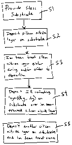
[0046] Fig. 2 is a flowchart illustrating certain steps carried out according
to
an example embodiment of this invention. Initially, a glass substrate is
provided (S1).
At least a layer of or including silicon nitride is then formed on the glass
substrate
(S2). This silicon nitride layer formed in S2 (step 2) may be formed either
directly on
and in contact with the glass substrate, or alternatively on the glass
substrate with
other layer(s) therebetween. The silicon nitride layer is ion beam treated
according to
any suitable ion beam treatment technique discussed herein (S3). For instance,
the
silicon nitride layer in S3 may be ion beam treated while the layer is being
sputter-
deposited (e.g., IBAD) and/or after the layer has been sputter-deposited
(e.g.,
peening). Following the ion beam treatment of the silicon nitride layer,
optionally a
contact layer comprising zinc oxide may be formed on the substrate. Then, an
IR
reflecting layer of a material such as silver is then formed (e.g., via
sputtering) on the
substrate over at least the ion beam treated silicon nitride layer (S4). Since
an ion
beam treated silicon nitride layer is located between at least the glass
substrate and the
IR reflecting layer, sodium migration from the glass substrate can be blocked
or
reduced during heat treatment thereby protecting the 1R reflecting layer from
the
same. After formation of the IR reflecting layer(s) on the glass substrate in
S4, it is
possible to form another layer of or including silicon nitride on the glass
substrate as
12
CA 02567048 2009-04-27
WO 20M M12189 pCTMgy rya
an overcoat or the lilts (S5). This additional silicon nitride layer (c.&,
wifetcoat) may
also be Ion beam treated in any auit ble manner discussed herein im ceder m
improve
durability Of the coated artincle, it is noted that these layers may be fanned
via
magnetron sputtering, IHAD, sputtering plus subsequent ice beam treattnent, or
in any
other suitable msaner f n different embodlmeata of this invention.
(00473 It is noted that any of the silicon nitride layers to be ion beam
treated
herein may be initially spatter deposited in any suitable atnichiometric form
including
but not limited to Si3N4 or a Si-rich type of silicon nitride. Example Si-rich
types of
silicon nitride are discussed in U.S. 200210064662 .
and any Si-rich layer discussed therein may be initially sputter-deposited
herein for
any suitable silicon nitride layer. Also, silicon nitride layers herein may of
course be
doped with ahmrinum (e.g., 1-10%) or the like in certain example embodiments
of
this invention.
(0048] Sputtering used for sputter-depositing silicon nitride in a
conventional
manner (e.g., via magnetron mttehng) is a relatively low energy process. As a
result, sputter-deposited silicon nitride layers are not pattkmlarly dense.
Moreover,
bnxxuae of the relatively low energy Involved in spa r-depositing silicon
nitride,
sputter-deposited silicon nitride layers typically suffer from weak Si-N bonds
since at
least certain amounts of nitrogen and up trapped In the layer in it macucr not
won-
bonded to silicon, and dangling Si bonds are present Unfoanmately, this
results in a
rather paaus layer which is prone to oxidation and/or sodium migration which
can
erase optical properties (n aa&or k) of trine layer and thus the coating to
significantly
change For example, oavIronmentai elements such ae water, humiditty, oxygen,
cemextt, and/orthe Pike tend to parse the optical properties of sputter-
deposited silicon
nitride to vary in an unpredictable mama thereby resulting in possible color
and/or
h'namiaaion changes. In certain example embodiments of this invention, the
afasessid problems with conventional sputter-deposited ate nitride layers are
addressed and remedied by ion treating the silicon nitride layer. Silicon
nitride
growth from ions has been found to be betas/ than growth ft m neutrals such as
in
sputtering, In paticular, the inc raasedktaetic energy obtained in ion
treating the
silicon nitride layer helps the layer to grow and/or form in a more dense
mariner
13
CA 02567048 2006-11-06
WO 2006/012185 PCT/US2005/022198
and/or with improved stoichiometry (e.g., with better Si-N bonding). The
higher
density and stronger bonds following ion treatment of the silicon nitride are
advantageous with regard to durability, sodium migration, and the like.
Moreover, it
has surprisingly been found that the excess nitrogen in the layer 3 as a
result of the
doping tends to reduce sodium migration during heat treatment.
[0049] It has also been found that ion beam treating of a layer comprising
silicon nitride increases the hardness of such a layer according to certain
example
embodiments of this invention (e.g., via IBAD or peening). A layer comprising
silicon nitride when conventionally sputtered typically has a hardness of from
10-14
GPa. In certain example embodiments of this invention however, when ion beam
treated, the silicon nitride layer realizes a hardness of at least 20 GPa,
more preferably
of at least 22 GPa, and most preferably of at least 24 GPa.
[0050] Figure 3 is a side cross sectional view of a coated article according
to
an example non-limiting embodiment of this invention. The coated article
includes
substrate 1 (e.g., clear, green, bronze, or blue-green glass substrate from
about 1.0 to
10.0 mm thick, more preferably from about 1.0 mm to 3.5 mm thick), and a low-E
coating (or layer system) 2 provided on the substrate 1 either directly or
indirectly.
The coating (or layer system) 2 includes, in this example embodiment:
dielectric
silicon nitride layer 3 (which may be ion beam treated) which may be of Si3N4,
nitrogen doped type, or of any other suitable stoichiometry of silicon nitride
in
different embodiments of this invention, first lower contact layer 7 (which
contacts IR
reflecting layer 9), first conductive and preferably metallic or substantially
metallic
infrared (IR) reflecting layer 9, first upper contact layer 11 (which contacts
layer 9),
dielectric layer 13 (which may be deposited in one or multiple steps in
different
embodiments of this invention), another silicon nitride layer 14, second lower
contact
layer 17 (which contacts 1R reflecting layer 19), second conductive and
preferably
metallic IR reflecting layer 19, second upper contact layer 21 (which contacts
layer
19), dielectric layer 23, and finally dielectric silicon nitride overcoat
layer 25 (which
may be ion beam treated). The "contact" layers 7, 11, 17 and 21 each contact
at least
one IR reflecting layer (e.g., layer based on Ag). The aforesaid layers 3-25
make up
low-E (i.e., low emissivity) coating 2 which is provided on glass or plastic
substrate 1.
14
CA 02567048 2010-01-15
WO 2SO"121 PCTM83wsbvm
$1Hiooo nude ieypr 25 i= tin oatermoetlayar d tts coo n 2. lawbe*a ttaam to
4.- - s 4 ietakh am dimcrdbwaed.9or aedsao !' etlLcas oi~dsideeWeivr lsYels 3
aod25.
In a coonbia humsoea, the aid wrists asckda ady ii. -
mbsinow I w IlTi tied In ft 3. Bows er, madoliddc coded aetkIce hawk owl be
wed is ds iom soot m famtowadieiide wtadebdeir 113 wkido ui , and Ike t6a.
A lsadasled vebiCie window awk m a ndndtfd &d iac "doe bw add second dlw
msiettt+lee knekeemed b ana ddnatho via a pollmn bamedIA U%W (e.1,. ado US
d,616.0l0}. ore of diets
mtlbeoatet of the istltiwee my atippctt eosbS 2 no in imedor =do= dosed in
coeds eeoemple ambodmentm. As fbdr I+C3 window m>ik so M window exit may
iodide tiro rpeced apart xianetees 1. Aaexsmpie IG window sit is tlwtta nd Md
daaibed, fareodaad ile. inlLS. PatiesttNo. 6,632.491.
AnuuvkK3 WhddetwdvaaMade.
farem;dshtpb. t e tweed gkaw obelnts 1 gamin ft 3 coupled to sadist yes
iubttuloe viaspsoai(s). me - ts) m' lire floe with a M bsieg ddku d
tQvbetwben.
Iii pp between the subumeas ie U3 acct o bmimoetamay ie omnsie rode ,esbe
Sfled with a pee mach u atp u (At). An sxemple 10 unit may oentpdse a pair of
mpedvd spat cow g1^s mTnstisees esdld shoat 4 =tbiet one of which ie cared
with
a eetab basic b ceete3a totsagii bmaadoes. wbeon t e g bsdwss tie wlstddaees
msybEdom tibeaE S m 3d dam, modepete/etmbly fmae mbtadt 10 b 20 aem, soda"
preaenibly shoat 16 am ltd aomtmin 4ugAs beeW cee, tie dos n 2 mq be provided
en the bmtdsr ardAhcs of Biker ao6rlteie fsaR Ws gap. .
NIa21 Ti catsb aodanapie embodbaethts of tics iavstioq, vets oar both ai nppds
soseora [e311 aotef w 21 n*y'be ev<i0edioe gds8edt 7>doa, at 1eea ar oflrBL?
iacineiin )awn 11 mdkr 11 maybe been ien bseen v ated with attest
oxypea ioam iR adder b oxldrioa peeled d-s acres in catatm ex emgle awbodl
meats of
chid kwaNfon.
(x163] lf+d^epie drupe elfetiidp 1o iigesm 3. ?.9.11.13,14, I?.19, 21.23 and
25 of the Fig. 3 coating ears dirceced In U.S. Patent No. 7,34,762.
CA 02567048 2006-11-06
WO 2006/012185 PCT/US2005/022198
example, dielectric layers 3 and 14 may be of or include silicon nitride in
certain
embodiments of this invention. Silicon nitride layers 3 and 14 may, among
other
things, improve heat-treatability of the coated articles, e.g., such as
thermal tempering
or the like. The silicon nitride of layers 3 and/or 14 may be of the
stoichiometric type
(Si3N4) type, nitrogen doped type as discussed herein, or alternatively of the
Si-rich
type in different embodiments of this invention. Any and/or all of the silicon
nitride
layers discussed herein may be doped with other materials such as stainless
steel or
aluminum in certain example embodiments of this invention. For example, any
and/or all silicon nitride layers discussed herein may optionally include from
about 0-
15% aluminum, more preferably from about 1 to 10% aluminum, most preferably
from 1-4% aluminum, in certain example embodiments of this invention. The
silicon
nitride may be deposited by sputtering a target of Si or SiAI in certain
embodiments
of this invention. Moreover, silicon nitride layer 3 may be ion beam treated
in any
manner discussed herein (e.g., with at least nitrogen ions via IBAD) in order
to reduce
sodium migration from the glass substrate toward the IR reflecting layer(s)
during
HT.
[0054] Infrared (IR) reflecting layers 9 and 19 are preferably substantially
or
entirely metallic and/or conductive, and may comprise or consist essentially
of silver
(Ag), gold, or any other suitable IR reflecting material. IR reflecting layers
9 and 19
help allow the coating to have low-E and/or good solar control
characteristics. The IR
reflecting layers may, however, be slightly oxidized in certain embodiments of
this
invention. Dielectric layer 13 may be of or include tin oxide in certain
example
embodiments of this invention. However, as with other layers herein, other
materials
may be used in different instances. Lower contact layers 7 and/or 17 in
certain
embodiments of this invention are of or include zinc oxide (e.g., ZnO). The
zinc
oxide of layer(s) 7, 17 may contain other materials as well such as Al (e.g.,
to form
ZnAlO,,). For example, in certain example embodiments of this invention, one
or
more of zinc oxide layers 7, 17 may be doped with from about 1 to 10% Al, more
preferably from about 1 to 5% Al, and most preferably about 2 to 4% Al. The
use of
zinc oxide 7, 17 under the silver 9, 19 allows for an excellent quality of
silver to be
achieved. Upper contact layers 11 and/or 21 may be of or include NiCr, NiCrOX
and/or the like in different example embodiments of this invention.
16
CA 02567048 2006-11-06
WO 2006/012185 PCT/US2005/022198
[0055] Dielectric layer 23 may be of or include tin oxide in certain example
embodiments of this invention. However, layer 23 is optional and need not be
provided in certain example embodiments of this invention. Silicon nitride
overcoat
layer 25 may be initially deposited by sputtering or IBAD, and may be ion beam
treated in any manner discussed herein.
[0056] Other layer(s) below or above the illustrated coating may also be
provided. Thus, while the layer system or coating is "on" or "supported by"
substrate
1 (directly or indirectly), other layer(s) may be provided therebetween. Thus,
for
example, the coating of Fig. 3 may be considered "on" and "supported by" the
substrate 1 even if other layer(s) are provided between layer 3 and substrate
1.
Moreover, certain layers of the illustrated coating may be removed in certain
embodiments, while others may be added between the various layers or the
various
layer(s) may be split with other layer(s) added between the split sections in
other
embodiments of this invention without departing from the overall spirit of
certain
embodiments of this invention.
[0057] While various thicknesses and materials may be used in layers in
different embodiments of this invention, example thicknesses and materials for
the
respective layers on the glass substrate 1 in the Fig. 3 embodiment are as
follows,
from the glass substrate 1 outwardly:
Example Materials/Thicknesses; Fig. 3 Embodiment
Layer Preferred Range (A) More Preferred (A) Example (A)
Glass (1-10 mm thick)
N-doped Si3N4 (layer 3) 40-450 A 70-250 A 100
ZnO,, (layer 7) 10-300 A 40-150 A 100
Ag (layer 9) 50-250 A 80-120 A 98
NiCrO,, (layer 11) 10-100 A 30-45 A 35
SnO2 (layer 13) 0-1,000 A 350-630 A 570
SiXNy (layer 14) 50-450 A 90-150 A 120
ZnO,
(layer 17) 10-300 A 40-150 A 95
Ag (layer 19) 50-250 A 80-220 A 96
NiCrO,, (layer 21) 10-100 A 30-45 A 35
17
CA 02567048 2006-11-06
WO 2006/012185 PCT/US2005/022198
Sn02 (layer 23) 0-750 A 150-300 A 200
N-doped Si3N4 (layer 25) 10-750 A 100-320 A 180
[0058] An example advantage of certain embodiments of this invention is that
ion beam treatment of silicon nitride layer 3 may permit a lesser thickness
layer 3 to
be used while still providing sufficient sodium migration barrier and/or
antireflection
properties. This may be advantageous in that a lesser thickness for layer 3
may permit
visible transmission to be increased in certain example instances which is
sometimes
desirable.
(0059] Referring to Figs. 2-4 and 6-8, an example method for making a coated
article according to an example embodiment of this invention will now be
described.
Initially, a glass substrate 1 is provided. Silicon nitride layer 3 is then
formed on the
substrate either via magnetron sputtering or via a combination of sputtering
and ion
beam treatment (e.g., via IBAD). As discussed above, the ion beam treatment of
silicon nitride layer 3 may be performed via IBAD and/or peening in different
embodiments of this invention. Fig. 4(a) illustrates an example of ion beam
treatment
via peening, whereas Figs. 4(b) and 8 illustrate an example of ion beam
treatment via
IBAD where the ion beam treatment occurs simultaneously with sputtering and
the
sputtered material from the target (e.g., Si or SiAl inclusive sputtering
target) and the
ion beam intersect proximate the surface where the layer is being formed.
[0060] Following formation of silicon nitride inclusive layer 3, underlying
layers 7, 9, 11, 13, 14, 17, 19, 21 and 23 are sputter deposited on the glass
substrate 1
in this order as shown in Fig. 3. Then, overcoat silicon nitride layer 25 is
deposited
on the substrate 1 over the underlying layers. As discussed above, the ion
beam
treatment of layer 25 may be performed via IBAD and/or peening in different
embodiments of this invention. Fig. 4(a) illustrates an example of ion beam
treatment
via peening, whereas Figs. 4(b) and 8 illustrate an example of ion beam
treatment via
IBAD where the ion beam treatment occurs simultaneously with sputtering and
the
sputtered material from the target (e.g., Si or SiAl inclusive sputtering
target) and the
ion beam intersect proximate the surface where the layer is being formed.
18
CA 02567048 2006-11-06
WO 2006/012185 PCT/1JS2005/022198
(0061] In post-sputter deposited peening embodiments, referring to Fig. 4(a)
for example, after a silicon nitride layer (3 and/or 25) has originally been
sputter
deposited, the originally deposited layer is ion beam treated with an ion beam
B as
shown in Fig. 4(a) to form ion beam treated layer. The ion beam B includes
injecting
at least nitrogen ions into the silicon nitride layer so as to cause at least
one of the
following to occur in the layer due to the ion beam treatment: (a) formation
of
nitrogen-doped Si3N4 in at least part of the layer, thereby reducing Si
dangling bonds
and susceptibility to oxidation; (b) creating a nitrogen graded layer in which
the
nitrogen content is greater in an outer portion of the layer closer to the
layer's outer
surface than in a portion of the layer further from the layer's outer surface;
(c)
improving anti-migration characteristics of the layer so that the layer is a
better
inhibitor of sodium migration during HT; (d) increasing the density of the
layer which
has been ion beam treated, (e) stress characteristics of the layer to be
improved, and/or
(f) reducing the amount and/or size of voids in the layer.
[0062] In certain post-sputtering peening embodiments (e.g., see Fig. 4(a)),
it
is desirable to sputter-deposit the silicon nitride layer in Si-rich form
prior to ion beam
treating so as to be characterized by SiN,,, where xis no greater than 1.30
(more
preferably no greater than 1.20, even more preferably no greater than 1.10,
still more
preferably no greater than 1.00). Then, after ion beam treatment with nitrogen
ions
during peening as shown in Fig. 4(a), the silicon nitride becomes more
stoichiometric
(i.e., x moves toward 1.33). Stoichiometric silicon nitride is characterized
by Si3N4
(i.e., x is 4/3 = 1.33). In certain example embodiments, following ion beam
treatment
the silicon nitride layer(s) (e.g., 3 and/or 25) may comprise Si3N4 which is
additionally doped with more nitrogen (i.e., N-doped Si3N4). In certain
example
embodiments, the Si3N4 may be doped with at least 0.1% (atomic %) nitrogen,
more
preferably from about 0.5 to 20% nitrogen, even more preferably from about 1
to 10%
nitrogen, and most preferably from about 2 to 10% nitrogen (or excess
nitrogen). In
certain example instances, the nitrogen doping may be at least about 2%
nitrogen
doping. Unlike the nitrogen in the Si3N4 of the layer, the excess nitrogen (or
the
doping nitrogen referenced above) is not bonded to Si (but may or may not be
bonded
to other element(s)). This nitrogen doping of Si3N4 may be present in either
the entire
19
CA 02567048 2009-04-27
WO 2MM12333 PCT(RS2tM2219a
layereompaiaing icon nitride, or alternatively in only a part of the
layereemprising
silicon nitride (e.g., proximate an upper enders thezeof in peeQnug
tm5odmeatn)
Imo) In IBAD ambodiaxnta, Figs. 4(b) and 8 illustr e t the loebeam
treanaem Is performed simult naoasty with s sm ing of Ilya 3 andhx 25.
Refezdng
to Pig. 8 In particular, this example embodiment of IBAD urea ion beam
assisted
apuu=g where the deposition device includes both a liner ion bum come(s) 26
and at feast one sputtering cathode (e g., magnodna cathode) 50 in a vactarm
chamber
at deposition chamber where the ion beam heated layer is deptmted by a
combination
of sputtering and ion beam The ice be= B (including c ions)
from the ion source 26 and the particles from the sputtering target(s) impinge
upon the
substrate err layer being famed in a common area. Preferably. the iae beam B
is
angled re3ative to a serrate of the mbatzmc at an aegis of from nba* 40 to 'TO
degrees
so as to Intersect the sputtered particles proximate the: substrate aotface.
While to
e hekaCe support in Fig. 8 is ilostrmed a WAS a rotating auppoee, s lineatr-
moving
eotveying support may be mow spproopciate in certain example a bodimuta of
this
invention. Again, the fan beemntremment uainglBABiraulta in at least nit ogcn
ions
being injected into the silicon nimde layer so an to cause at least one of the
following
to occur in the layer (3 and/or 25) due to the nom beam Weatomt: (a) formation
of
nitrogen-doped Si in at learnt pet of doe hirer (pat:i+et Ny mrcgghow the
layer,
thereby reducing SI dangling bonds and susceptibility to orrlioe; (b)
Improving
anti-n, ation characteristics of the layer so that the layer is a better
iainbitor of
sodium migration doing 13T; (c) imxeaaiag the duty of the layer which has been
ism beam treated, (d) strew cheracteriadca of the layer to be improved, and/or
(o)
reducing the amount and/or size of voids in the layer.
10064] In oesWn example embodrmemta of this invention, cue arboth of I~TICr
or13iCrO1 layers 11 andta 21 may be ion beam treatedaateg at last mygen Wain
order to oxidation grade a desatibed in U.S. Patent Application No.
2005!0258029,
I0 6J Referring to Pigs. 2.4 and 6.8, the ion beam B is generated by ism
aounx 26, and introduces at least nitrogen lens into the silicon nitride layer
(3 andfar
25) As explained above, an anode-cathode energy at the source is utilized
which
CA 02567048 2009-04-27
WO 20061012186 PCT1US2055/022198
trandadea luau an ion energy suit" to cause the stags of the silicon nitride
layer to
tad upcw yeaezwn, at to amen teaosilo aaresm to be teduced cratethe ion bairn
treatment in certain ewnple embodiments of this invention (whether peening or
MAD is wed)õ the ion beam tteatmenitmay be fen n about 1-30 seconds, more
prrably firm about 1.20 seconds, to achieve dashed tesalta.
(0966] Figures 6-7 illustrate an exemplary linear or direct ion beam source 26
which may be used to ion beam treat layer(s) 3 andlor 25 with at imt nitrogen
ions in
eeatsin example embodiments (peening or l$AD). Loa basal aamoe (cc for aerate)
26
includes gaslpower inlet 31, aacatrack-shaped nods 27, gxoutrded cathode
magnet
portion 28, magnet poles, and Insulators 30. An electric gap is defined
between the
anode 27 and the cathode 29. A 3kV or any other actable DC power supply may be
used for source 26 in some embodiments. The gei(a) dWoossed ha:dn far 9se in
the
ion aowce during the ion bean, treatment maybe introduced into the source via
gee
inlet 31, or via any other suitable location. Ion beam source 26 is bated upon
a
known gridlams ion solace design. The linear source may include a linear shell
(which
is the cathode and grounded) inside of which has a cocixattic anode (which is
at a
positive puteatial). T is geometry of cathode-anode and magnetic field 33 may
give
rise to a close drift condition. Feedstock guises (e.g., nit ogee, argon.
oxygen, a
mixture of nitrogen and argon, etc) maybe fed through the cavity 41 between
the
anode 27 and cathode 29. The electrical energy between the anode and cathode
cracks the gato produce a plasma within the source. The ions 34 (&S, nitrogen
ions)
am expelled out (e.g., due to the nitrogs gas in the source) and directed
toward the
layer to be ion" erme traamd in the form of an ion beam. The ion beam maybe
dift'used, collimated, or focused. Example ions 34 in bear, (B) are shown in
Figure 6.
[00i7) A r source as long as O.5 to 4 maters maybe made sad usedin
certain example mAsacee, although aouroes of different lengths are anticipated
in
different its of this intention. Flom, layer 33 is shown in Pigare 6 and
completes the circuit thereby permitting the ion beam source to itmcdm
properly.
Example but non-lmimhg ion bean sources that maybe used to that layers herein
as
diaciosed in U.S. Patent Document Nos. 6,303.226, 6,359,3$8, mdln2004i(V67363,
21
CA 02567048 2006-11-06
WO 2006/012185 PCT/US2005/022198
[0068] In certain example embodiments of this invention, coated articles
herein may have the following optical and solar characteristics when measured
monolithically (before any optional HT). The sheet resistances (RS) herein
take into
account all IR reflecting layers (e.g., silver layers 9, 19).
Optical/Solar Characteristics (Monolithic; pre-HT)
Characteristic General More Preferred Most Preferred
RS (ohms/sq.): <= 6.0 <= 3.0 <= 2.8
En: <= 0.09 <= 0.04 <= 0.03
T,,15 (Ill. C 2 ): >= 70% >= 75% >= 75.5%
[0069] In certain example embodiments, coated articles herein may have the
following characteristics, measured monolithically for example, after heat
treatment
(HT):
Optical/Solar Characteristics (Monolithic; post-HT)
Characteristic General More Preferred Most Preferred
R. (ohms/sq.): <= 5.5 <= 2.5 <= 2.1
En: <= 0.08 <= 0.04 <= 0.03
T,,i5 (Ill. C 2 ): >= 70% >= 75% >= 80%
Haze: <= 0.40 <= 0.35 <= 0.30
[0070] Moreover, in certain example laminated embodiments of this
invention, coated articles herein which have been heat treated to an extent
sufficient
for tempering and/or heat bending, and which have been laminated to another
glass
substrate, may have the following optical/solar characteristics:
Optical/Solar Characteristics (Laminated; post-HT)
Characteristic General More Preferred Most Preferred
Rs (ohms/sq.): .<= 5.5 <= 2.5 <= 2.1
En: <= 0.08 <= 0.04 <= 0.03
Tõ;5 (Ill. D65 10 ): >= 70% >= 75% >= 77%
Haze: <= 0.45 <= 0.40 <= 0.36
[0071] Moreover, coated articles including coatings according to certain
example embodiments of this invention have the following optical
characteristics
22
CA 02567048 2006-11-06
WO 2006/012185 PCT/US2005/022198
(e.g., when the coating(s) is provided on a clear soda lime silica glass
substrate 1 from
I to 10 mm thick; e.g., 2.1 mm may be used for a glass substrate reference
thickness
in certain example non-limiting instances) (laminated).
Example Optical Characteristics (Laminated: post-HT)
Characteristic General More Preferred
T,i, (or TY)(Ill. D65 10 ): >= 75% >= 77%
a*t (Ill. D65 10 ): -6 to +1.0 -4 to 0.0
b*t (Ill. D65 10 ): -2.0 to +8.0 0.0 to 4.0
L* (Ill. D65 10 ): 88-95 90-95
RfY (Ill. C, 2 deg.): 1 to 12% 1 to 10%
a*f (Ill. C, 2 ): -5.0 to +2.0 -3.5 to +0.5
b*f (Ill. C, 2 ): -14.0 to +10.0 -10.0 to 0
L* (Ill. C 2 ): 30-40 33-38
RgY(I11.C,2deg.): 1to12% 1to10%
a*g (Ill. C, 2 ): -5.0 to +2.0 -2 to +2.0
b*g (Ill. C, 2 ): -14.0 to +10.0 -11.0 to 0
L* (Ill. C 2 ): 30-40 33-38
[0072] The following examples are provided for purposes of example only
and are not intended to be limiting.
EXAMPLES 1-3
[0073] Examples 1-3 illustrate example techniques for forming layers 3 and/or
25, or any other suitable layer according to example embodiments of this
invention.
Examples 1-3 utilized 1BAD type of ion beam treatment, and were made and
tested as
follows. A silicon nitride layer was deposited on a quartz wafer (used for
ease of
stress testing) using 113AD (e.g., see Fig. 8) under the following conditions
in the
deposition chamber: pressure of 2.3 mTorr; anode/cathode ion beam source
voltage
of about 800 V; Ar gas flow in the ion source of 15 sccm; N2 gas flow in the
ion
source 26 of 15 sccm; sputtering target of Si doped with about 1% boron; 460 V
applied to sputtering cathode; 5.4 sputtering amps used; 60 sccm Ar and 40
sccm N2
gas flow used for sputtering gas flow; linear line speed of 50 inches/minute;
where the
23
CA 02567048 2006-11-06
WO 2006/012185 PCT/US2005/022198
quartz wafer substrate was circular in shape and about 0.1 to 0.15 mm thick.
The ion
beam treatment time for a given area was about 3 seconds.
[0074] Example 2 was the same as Example 1, except that the anode/cathode
voltage in the ion source was increased to 1,500 V.
[0075] Example 3 was the same as Example 1, except that the anode/cathode
voltage in the ion source was increased to 3,000 V.
[0076] The stress results of Examples 1-3 were as follows, and all realized
compressive stress:
Example Compressive Stress Ion Source Anode/Cathode Volts
1 750 MPa 800 V
2 1.9 GPa 1,500 V
3 1 GPa 3,000 V
[0077] It can be seen from Examples 1-3 that the compressive stress of the
silicon nitride layer realized due to IBAD deposition is a function of ion
energy (i.e.,
which is a function of voltage applied across the anode/cathode of the ion
source 26).
In particular, 1,500 anode-cathode volts caused the highest compressive stress
to be
realized, whereas when too much voltage was applied the stress value began
moving
back toward tensile.
EXAMPLE 4
[0078] Example 4 used post-sputtering peening type of ion beam treatment,
and was made and tested as follows. A silicon nitride layer about 425 A thick
was
deposited by conventional magnetron-type sputtering using a Si target doped
with Al
on a substrate. After being sputter-deposited, the silicon nitride layer had a
tensile
stress of 400 MPa as tested on the quartz wafer. After being sputter-deposited
and
stress tested, the silicon nitride layer was ion beam treated using an ion
source 26 as
shown in Figs. 6-7 under the following conditions: ion energy of 750 eV per N
ion;
treatment time of about 18 seconds (3 passes at 6 seconds per pass); and N2
gas used
in the ion source. After being ion beam treated, the silicon nitride layer was
again
tested for stress, and had a tensile stress of only 50 MPa. Thus, the post-
sputtering
24
CA 02567048 2006-11-06
WO 2006/012185 PCT/US2005/022198
ion beam treatment caused the tensile stress of the silicon nitride layer to
drop from
400 MPa down to 50 MPa (a drop of 87.5%).
EXAMPLE 5
[0079] The following hypothetical Example 5 is provided for purposes of
example only and without limitation, and uses a 2.1 mm thick clear glass
substrates so
as to have approximately the layer stack set forth below and shown in Fig. 3.
The
layer thicknesses are approximations, and are in units of angstroms (A).
Layer Stack for Example 5
Layer Thickness (A)
Glass Substrate
N-doped Si3N4 100
ZnAlO.1109
Ag 96
NiCrO2, 25
Sn02 535
Si,,Ny 126
ZnAlO1115
Ag 95
NiCrO,, 25
Sn02 127
N-doped Si3N4 237
[0080] The processes used in forming the coated article of Example 5 are set
forth below. The sputtering gas flows (argon (Ar), oxygen (0), and nitrogen
(N)) in
the below table are in units of sccm (gas correction factor of about 1.39 may
be
applicable for argon gas flows herein), and include both tuning gas and gas
introduced
through the main. The line speed was about 5 m/min. The pressures are in units
of
mbar x 10"3. The silicon (Si) targets, and thus the silicon nitride layers,
were doped
with aluminum (Al). The Zn targets in a similar manner were doped with about
2%
Al.
CA 02567048 2006-11-06
WO 2006/012185 PCT/US2005/022198
Sputtering Process Used in Example 5
Cathode Target Power(kW) Ar 0 N Volts Pressure
IBAD N-doped Si3N4 layer 3 formed using any of Examples 1-4
C14 Zn 19.5 250 350 0 276 2.24
C15 Zn 27.8 250 350 0 220 1.88
C24 Ag. 9.2 250 0 0 541 1.69
C25 NiCr 16.5 350 0 0 510 2.33
C28 Sn 27.3 250 454 350 258 2.30
C29 Sn 27.3 250 504 350 246 1.97
C39 Sn' 30 250 548 350 257 2.29
C40 Sn 28.5 250 458 350 245 2.20
C41 Sn 30.8 250 518 350 267 2.45
C43 Si 59.7 350 0 376 285 2.47
C45 Zn 26.9 250 345 0 209 3.78
C46 Zn 26.8 250 345 0 206 1.81
C49 Ag 9.8 150 0 0 465 1.81
C50 NiCr 16.6 250 75 0 575 1.81
C54 Sn 47.3 250 673 350 314 1.92
IBAD N-doped Si3N4 layer 25 formed using any of Examples 1-4
[0081] It can be seen that in the aforesaid Example 5 both of silicon nitride
layers 3 and 25 were ion beam treated in a manner so as to cause N-doping of N-
doped Si3N4 to occur in each of the layers. However, although only one (either
one)
of such layers needs to be ion beam treated in certain other embodiments of
thins
invention.
[0082] After being sputter deposited onto the glass substrates, the Example 5
coated article was heat treated in a manner sufficient for tempering and heat
bending,
and following this heat treatment had the following characteristics as
measured in
monolithic form.
Characteristics of Example 5 (Monolithic; post - HT)
Characteristic Example 5
26
CA 02567048 2006-11-06
WO 2006/012185 PCT/US2005/022198
Visible Trans. (Ti,, or TY)(Ill. C 2 deg.): 80.0%
a* -4.8
b* 10.7
Glass Side Reflectance (RY)(Ill C, 2 deg.): 8.3%
a* -3.5
b* 7.8
Film Side Reflective (FY)(Ill. C, 2 deg.): 7.5%
a* -5.8
b* 14.2
RS (ohms/square) (pre-HT): 2.74
R5 (ohms/square) (post-HT): 2.07
Haze: 0.28
[0083] The coated article of Example 5 was then laminated to another
corresponding heat treated and bent glass substrate to form a laminated
vehicle
windshield product. Following the lamination, the resulting coated article
laminate
(or windshield) had the following characteristics.
Characteristics of Example 5 (Laminated; post - HT)
Characteristic Example 5
Visible Trans. (T,,1 or TY)(Ill. D65 10 ): 77.8%
a* -3.1
b* 3.5
Glass Side Reflectance (RY)(Ill C, 2 deg.): 9.0%
a* 1.5
b* -9.1
Film Side Reflective (FY)(Ill. C, 2 deg.): 8.9%
a* -1.1
b* -7.8
RS (ohms/square) see above
Haze: 0.32
27
CA 02567048 2006-11-06
WO 2006/012185 PCT/US2005/022198
[00841 While the aforesaid Examples ion beam treat layers comprising silicon
nitride, this invention is not so limited. Other layers may be ion beam
treated for
grading or otherwise ion beam treated in a similar manner.
[0085] Additionally, while the aforesaid embodiments use at least nitrogen
ions to ion beam treat layers of or including silicon nitride, this invention
is not so
limited. In this regard, for example, Fig. 5 illustrates another example
embodiment of
this invention. The Fig. 5 embodiment is the same as any peening embodiment
described above, except that oxygen ions are used to ion beam treat any
suitable
silicon nitride layer (e.g., for any of layers 3 and/or 25). In this
embodiment, the ion
beam treating of the silicon nitride overcoat or other suitable layer
transforms the
layer into a silicon oxynitride layer. This may be advantageous in certain
example
instances, because this could result in a coated article having higher visible
transmission and/or less reflectance. In Fig. 5, the "o" elements in the
silicon
oxynitride layer represent oxygen, whereas the "N" elements in the layer
represent
nitrogen. In Fig. 5, the silicon oxynitride layer is oxidation graded due to
the ion
beam treatment so that the layer is less oxided at a location closer to the
underlying
layer(s) than at a position further from the underlying layer(s). In other
words, in
oxidation graded embodiments, there is more oxygen in the layer provided
closer to
the exterior surface of the coated article than at a location at an inwardly
located
portion of the silicon oxynitride layer; this is because the ion energy used
in the ion
beam treatment causes many of the oxygen ions to penetrate the layer but not
go all
the way therethrough with many of the oxygen ions ending up near the outer
portion
of half of the layer. In certain example embodiments, only oxygen gas is fed
through
the ion source in this embodiment, whereas it is also possible to use other
gases in
addition to oxygen in certain alternative embodiments.
[0086] Thus, in the Fig. 5 embodiment where the silicon oxynitride layer is
oxidation graded, the ion energy is chosen so that the oxygen ions do not all
penetrate
the entire thickness of the layer being treated. In other words, an ion energy
is chosen
so that a portion of the layer is more oxidized further from the substrate
than is a
portion of the layer closer to the substrate. In still further embodiments of
this
invention, a combination of both oxygen and nitrogen gas may be used in IBAD
28
CA 02567048 2009-04-27
WO 200610121" t tasnosazusa
embodimens disomsed above for ton beam ti m l It of eertan layers sock as
Isyecs
spume cd from Si inclusive targets (this could also be used to fain, at
silicon oxynitride
layer).
(008; In certain other embodinsa' of thin tnvendpn, any of the aforesaid
embodiments may be applied to other coatings. For example and without
limitation,
any of the aforesaid ambodhaents may also be applied to coated Articles and
that solar
coottol coatfnge of one of mom of U.S. FalentDocument Noe. 200310150711.
2003/0194570, 6,723,211, 6,576,349, 5,514,476, 5,425,861.
In other worth, the aver oat layers snd/or lower
silicon mutts layers of any of 200310150711.200310194370, 6,723,211, 6376349,
3,514,476, and/or 5.425,861, or any other suitable caadn& may be ion beam
treated
acceding to any of the aforesaid a nbodbne its of this invention.
I0058] While many of the above-hand etabodi eta acs used in the coolant of
coated articles with solar control coatings, this invention is not so limited
Far
example. ion beam treWag of l*ye s as diacoesad bar in may also be used in the
context of other types of product and waft p relating thereto.
(0089] While the invention bas been described in connection with what is
pcaendy canddered to be the mad pm c" and prdeaed erobodiimeat, it is to be
understood that'the invention is not to be limited to the disclosed embodtmeot
but on
the contrary, is intended to cover various modi&adona and equivalent ants
included within the spirit and scope d the appended claims.
29