Note: Descriptions are shown in the official language in which they were submitted.
CA 02568315 2006-11-24
WO 2005/122376 PCT/KR2005/001768
Description
METHOD FOR SWITCHING LOW-POWER USING AC AND
SYSTEM FOR PERFORMING THE SAME AND POWER
SUPPLY FOR USING THE SYSTEM
Technical Field
[1] The present invention relates to a power control method using alternating
current
power, a system for performing the method and a power supply using the system,
which can stably control alternating current power to 0%-100% of the power
level
thereof when supplying low voltage alternating current power directly from
commercial alternating current power, thus having optimal efficiency, and
which
enable the integration of component circuits.
Background Art
[2] Generally, power control using Alternating Current AC power employs a zero-
crossing control method and a phase control method. In the zero-crossing
control
method, when voltage is zero, that is, when AC power advancing while forming a
sine
wave advances by one cycle and reaches point A having zero voltage, as
illustrated in
FIG. 1A, On/Off control is performed. In order to supply 50% of supplied AC
power,
power is controlled in such a way as to repeat an On/Off operation every cycle
in the
zero-crossing control method.
[3] Such a zero-crossing method is superior from the point of view of power
noise.
However, the zero-crossing method requires a circuit for finding the zero
point of AC
power, that is, the point where voltage is zero after a cycle has completed,
so that
economical efficiency is low. Accordingly, the zero-crossing method can be
utilized
for expensive equipment, but has a disadvantage in that uniform power is not
supplied
in power control in which a control rate is low compared to the amount of AC
power.
[4] The phase control method controls power, which is supplied to a load, by
varying
the phase of supplied AC power as shown in FIG. 1B, so that the method is
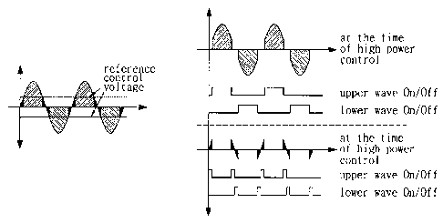
simple and,
thus, may be used throughout all of industry. However, the phase control
method has
disadvantages in that noise is high and the method is not stable for power
control for
less than 50% of supplied AC power because switching on and off is performed
at high
voltage positions, and uniform power is not supplied.
[5] That is, the conventional zero-crossing method and phase control method
perform
the On/Off control of power based on phase according to time, whereas a novel
method proposed by the present invention performs the On/Off control of power
based
on the amount of voltage.
Disclosure of Invention
1
CA 02568315 2006-11-24
WO 2005/122376 PCT/KR2005/001768
Technical Problem
[6] The present invention has been invented so as to overcome the
disadvantages of the
zero-crossing method and the phase control method, and a first object of the
present
invention is to provide a power control method, which can uniformly and stably
control supplied AC power, and enables a super-small size circuit to be
implemented
so as to achieve optimal technical efficiency and economic efficiency at the
time of
supplying required power while controlling AC power.
[7] Furthermore, a second object of the present invention is to provide a
power control
system that is composed of integrated circuits that prevents excessive current
from
being applied to loads by frequently supplying low level voltage.
[8] Furthermore, a second object of the present invention is to provide a
power supply
using the power control system that is composed of integrated circuits.
Technical Solution
[9] In order to achieve the first object, the present invention provides a
power control
method using Alternating Current (AC) power, the method being capable of
performing: low power control that passes only two portions of (+) positive
direction
waves of each one-cycle sine wave of the AC power and only two portions of (-)
negative direction waves of each one-cycle sine wave of the AC power, which
have
voltage levels lower than a set reference voltage level, through a system; and
high
power control that does not pass only two portions of (+) positive direction
waves of
each one-cycle sine wave of the AC power and only two portions of (-) negative
direction waves of each one-cycle sine wave of the AC power, which have
voltage
levels lower than a set reference voltage level, through the system.
[10] In order to achieve the second object, the present invention provides a
power
control system using AC power, including:
[11] a rectifier unit configured to full-wave-rectify input AC power and
composed of
bridge diodes;
[12] a voltage level detection unit connected to the rectifier unit, and
configured to set
reference control voltage and output a signal according to a set control
criterion;
[13] a phase determination unit configured to control the switching operation
of the
input AC power according to the amount of the reference control voltage set by
the
voltage level detection unit;
[14] a power control unit connected to the voltage level detection unit and
the phase de-
termination unit, and configured to switch on and output parts of the power,
which
have voltage levels lower than the reference control voltage, at the time of
low power
control, and switch on and output parts of the power, which have voltage
levels higher
than the reference control voltage, at the time of high power control; and
2
CA 02568315 2006-11-24
WO 2005/122376 PCT/KR2005/001768
[15] an excessive current detection unit connected to the output side of the
power control
unit, and configured to serve as a protection circuit for cutting off supply
of power
when excessive current is included in the output power.
[16] Furthermore, in order to achieve the third object, the present invention
provides a
power supply constructed by connecting a transformer to output terminals of
the power
control system and connecting a known rectifying and smoothing circuit or
constant
voltage circuit to output terminals of the transformer, wherein the power
supply
operates to vary the voltage of AC power, which is detected through the power
control
system, using the transformer, and to convert the varied voltage into direct
current
voltage using the rectifying and smoothing circuit or constant voltage
circuit.
[17] The present invention is connected between the loads of power supply
terminals
and supplies power through direct switching operation, so that it has minimal
loss and
a simple construction.
Brief Description of the Drawings
[18] FIGS. 1A and 1B are waveform diagrams illustrating a zero-crossing method
and a
phase control method that are used for general power control;
[19] FIG. 2 is a waveform diagram illustrating a power control method
according to the
present invention;
[20] FIG. 3 is a block diagram illustrating the construction of a power
control system
according to the present invention;
[21] FIG. 4 is an embodiment of a circuit that implements the power control
system
according to the present invention;
[22] FIG. 5 is a waveform diagram in the case where the power control system
according
to the present invention outputs low power having low voltage levels;
[23] FIG. 6 is a waveform diagram in the case where the power control system
according
to the present invention outputs high power having high voltage levels;
[24] FIG. 7 is a waveform diagram illustrating the various waveforms of
voltages output
from the power control system of the present invention at the time of low
power
control;
[25] FIG. 8 is a waveform diagram illustrating the various waveforms of
voltages output
from the power control system of the present invention at the time of high
power
control; and.
[26] FIG. 9 is a block diagram illustrating an embodiment in which a power
supply is
implemented using the power control system of the present invention.
Best Mode for Carrying Out the Invention
[27] With reference to the accompanying drawings, preferred embodiments of the
present invention are described in detail below.
3
CA 02568315 2006-11-24
WO 2005/122376 PCT/KR2005/001768
[28] FIG. 2 is a waveform diagram illustrating a power control method
according to the
present invention, FIG. 3 is a block diagram illustrating the construction of
a power
control system according to the present invention, FIG. 4 is an embodiment of
a circuit
that implements the power control system according to the present invention,
FIG. 5 is
a waveform diagram in the case where the power control system according to the
present invention outputs low power having low voltage levels, FIG. 6 is a
waveform
diagram in the case where the power control system according to the present
invention
outputs high power having high voltage levels, and FIG. 7 is a block diagram
il-
lustrating an embodiment in which a power supply is implemented using the
power
control system of the present invention.
[29] The power control method according to the present invention, as shown in
FIG. 2,
sets a power level for the sine waveform of input AC power, and, in high power
control in which a power level required at output terminals is below 50% of
the power
level of input AC power, switches on only the portions of (+) positive
direction waves
and (-) negative direction waves having power levels lower than a set power
level and
passes the portions through the system.
[30] Furthermore, in high power control in which a power level required at
output
terminals is above 50% of the power level of the input AC power, control is
performed
such that only the portions of (+) positive direction waves and (-) negative
direction
waves having power levels higher than the set power level are switched on and
passed
through the system.
[31] Accordingly, in the entire power control, control is performed such that
the On/Off
control of AC power is performed at low power level portions, so that
switching noise
is low compared to the phase control method in which On/Off control is
performed at
high power level portions, and four switching operations are performed in each
one-
cycle waveform of AC power, that is, (+) positive direction waves and (-)
negative
direction waves, so that output having even voltage levels are performed
compared to
the zero-crossing method.
[32] As shown in FIG. 3, in the power control system according to the present
invention,
a rectifier unit 100 for full-wave-rectifying commercial AC power is connected
to
output terminals for commercial AC power, and a voltage level detection unit
110 for
detecting the voltage level of a sine waveform is connected to the output
terminal of
the rectifier unit 100. A phase determination unit 120 for performing
switching on/off
according to the detected voltage level is connected to the output terminal of
the
detection unit 120. The phase determination unit 120 prevents the output of
low power
when the phase of the input AC power is higher than the voltage level set by
the
voltage level detection unit 110, and prevents the output of high power when
the phase
of the input AC power is lower than the voltage level set by the voltage level
detection
4
CA 02568315 2006-11-24
WO 2005/122376 PCT/KR2005/001768
unit 110, thus operating such that power control is achieved at a low voltage
level.
[33] A power control unit 130 for performing switching so as to pass part of
input AC
power, which has power levels necessary at an output side, therethrough is
connected
to the output side of the voltage level detection unit 110. An excessive
current
detection unit 140 serving as a protection circuit for cutting off supply when
excessive
current flows is connected to the power control unit 130, and the excessive
current
detection unit 140 is connected to a second rectifier unit 150 for full-wave-
rectifying
AC power.
[34] Assuming that only 10% of input AC power is required (for example, input
AC
power is 100V and required power is lOV), the present invention constructed as
described above employs a method of repeating a time period in which the power
control unit 110 passes voltage in the above range through the system and a
time
period in which the power control unit 110 does not pass voltage above the
above
range through the system until the voltage level detection unit 120 detects
low voltage
power level below 20% of the input AC power, thus supplying 10% of the input
power, not the conventional power control method in which 100% of the power is
passed through the system and a non-conduction time period ten times a
conduction
time period is provided, thus reducing the evenness of output power.
Accordingly, the
present invention is a method of supplying power having considerably improved
evenness in power supply, and a method capable of replacing transformers in
many ap-
plications.
[35] The power control system according to the present invention may be
implemented
using a circuit as shown in FIG. 4, and the circuit of FIG. 4 is composed of a
switching
circuit that is composed of a simple circuit without a holding circuit, which
operates
like a triac or SCR.
[36] The rectifier unit 100 is composed of bridge diodes D1-D4, which are
connected to
an output terminal for commercial AC power, and full-wave-rectifies the
commercial
AC power.
[37] In the construction of the voltage level detection unit 110, smoothing
resistors R2
and R3 are connected to both ends of a variable resistor R1 connected to the
output
side of the bridge diodes D1-D4 of the rectifier unit 100. A variable resistor
VR 1 is
constructed to output signals between a pair of resistors R3 and R4 connected
in series
and between another pair of resistors R5 and R6 connected in series. The base
terminal
of a PNP-type second transistor Q2 is connected between a pair of resistors R3
and R4,
and the base terminal of an NPN-type first transistor Q1 is connected between
another
pair of resistors R5 and R6.
[38] In the construction of the power control unit 130, the base terminal of a
PNP-type
third transistor Q3 is connected to the emitter terminal of the second
transistor Q2 of
CA 02568315 2006-11-24
WO 2005/122376 PCT/KR2005/001768
the voltage level detection unit 110, the emitter terminal of the third
transistor Q3 is
connected to an first side output terminal of the bridge diodes D 1-D4, and
the
collector terminal of the third transistor Q3 is connected to an second side
output
terminal of the bridge diodes D1-D4 through a plurality of resistors R9, R10
and R11.
The base terminal of a PNP-type fifth transistor Q5 is connected to the
collector
terminal of the first transistor Q1 of the voltage level detection unit 110
through a
resistor R8, the emitter terminal of the fifth transistor Q5 is connected to a
first side
output terminal of the bridge diodes D 1-D4, and the collector terminal of the
fifth
transistor Q5 is connected to a second side output terminal of the bridge
diodes D 1-D4
through a plurality of resistors R13 and R16. The base terminal of the fourth
transistor
Q4 is connected between the appropriate ones R9 and R10 of resistors R9, R10
and
R11 connected to the collector terminal of the third transistor Q3, the
emitter terminal
of the fourth transistor Q4 is connected to a first side output terminal of
the bridge
diodes D 1-D4, and the collector terminal of the fourth transistor Q4 is
connected to an
second side output terminal of the bridge diodes D 1-D4 through a plurality of
resistors
R14 and R15. The base terminal of the sixth transistor Q6 is connected between
resistors R13 and R16 connected to the collector terminal of the fifth
transistor Q5, the
emitter terminal of the sixth transistor Q6 is connected to a first side
output terminal of
the bridge diodes D 1-D4, and the collector terminal of the sixth transistor
Q6 is
connected to an second side output terminal of the bridge diodes D1-D4 through
a
plurality of resistors R17 and R18. The base terminal of a ninth transistor Q9
is
connected between resistors R17 and R18, which are connected to the collector
terminal of the sixth transistor Q6, through the diode D14, and between
resistors R14
and R15, which are connected to the collector terminal of the fourth
transistor Q4,
through a diode D13. The emitter terminal of the ninth transistor Q9 is
connected to a
first side terminal of the bridge diodes D 1-D4. The collector terminal of the
ninth
transistor Q9 is constructed to provide input to the base terminal of a tenth
transistor
Q10 so as to switch on and off power to load terminals AC3 and AC4 through a
resistor R25.
[39] In this case, the phase determination unit 120 is constructed such that
the base
terminal of a seventh transistor Q7 is connected to a diode D11, which is
connected to
the variable resistor VR 1 of the voltage level detection unit 110, through
resistors R20
and R21, the collector terminal of the seventh transistor Q7 is connected to
the base
terminals of the fourth transistor Q4 and the eighth transistor Q8 through the
diode
D 12 and the resistor R8, and the collector terminal of the eighth transistor
Q8 is
connected to the base terminal of the sixth transistor Q6.
[40] In the power control circuit constructed as described above, in
accordance with the
present invention, when commercial AC power is applied through terminals AC1
and
6
CA 02568315 2006-11-24
WO 2005/122376 PCT/KR2005/001768
AC2, AC power advancing while forming a sine wave is converted into a full-
wave-rectified waveform through the bridge diodes D 1-D4 of the rectifier unit
100.
For the waveform full-wave-rectified by the bridge diodes D 1-D4, the voltage
level
for the switching on and off of the AC power waveform is set according to the
value of
the variable resistor VR1 of the voltage level detection unit 110.
[41] When a full-wave-rectified waveform having power levels higher than a
value set
through the variable resistor VR1 is input, the first transistor Q1 connected
to the
output side of the variable resistor VR1 of the voltage level detection 110 is
turned on
and, thus, the fifth transistor Q5 of the power control unit 130 is turned on
and the
sixth transistor Q6 connected to the collector terminal of the transistor Q5
is also
turned on. As the sixth transistor Q6 is turned on, the sixth transistor Q6
connected to
the collector terminal of the transistor Q5 is turned on. As the sixth
transistor Q6 is
turned on, power maintained at the resistor R19 of the power control unit 130
is
applied to the base terminal of the switching transistor Q9 through the diode
D14 and,
thus, the ninth transistor Q9 is turned on. Accordingly, the tenth transistor
Q10 is
turned on, so that only power having voltage levels higher than the value
(reference
control voltage) set through the variable resistor VR1 is output through
output
terminals AC3 and AC4. That is, as shown in FIG. 2, high power having voltage
levels
higher than the reference control voltage set by the variable resistor VR1 is
output. At
this time, when the first transistor Q1 of the voltage level detection unit
110 operates,
the second transistor Q1 is also turned on and, thus, turns off the third
transistor Q3 of
the power control unit 130.
[42] In the above case, when a voltage level required at the load terminals is
below 50%
of the voltage level of input power, that is, the value of the variable
resistor VR1 of the
voltage level detection unit 110 is set so as to pass only low power, which is
below
50% of the power level of input AC power, through the variable resistor VR1,
power
applied to resistors R3-R6 through the variable resistor VR1 is relatively
low, so that
the first transistor Q1 of the voltage level detection unit 110 does not
operate and the
second transistor Q2 also does not operate. Accordingly, the third transistor
Q3 of the
power control unit 130 is turned on. As the third transistor Q3 is turned on,
the fourth
transistor Q4 is turned on. As the fourth transistor Q4 is turned on, power
maintained
at the resistor R19 of the power control unit 130 is applied to the base
terminal of the
ninth transistor Q9 through a diode D13 and, thus, the ninth transistor Q9 is
turned on.
Accordingly, the tenth transistor Q10 is turned on and, thus, only low power
having
voltage levels lower than the value (reference control voltage) set through
the variable
resistor VR1 is output through the output terminals AC3 and AC4.
[43] In the case where the voltage level set by the voltage level detection
unit 110 is high
(in the case of high power output) as shown in FIG. 6, a signal is applied to
the base
7
CA 02568315 2006-11-24
WO 2005/122376 PCT/KR2005/001768
terminal of the seventh transistor Q7 of the determination unit 120 through
the variable
resistor VR1 and diode D11 of the voltage level detection unit 110 and, thus,
the
seventh transistor Q7 is turned on. Accordingly, the power applied to the base
terminal
of the fourth transistor Q4 of the power control unit 130 is cut off and,
thus, the fourth
transistor Q4 is turned off, thus preventing power having voltage levels lower
than the
value (reference control value) set by the variable resistor VR1 from being
output. At
this time, the eighth transistor Q8 of the phase determination unit 120 is
turned off.
[44] Furthermore, in the case where the voltage level set by the voltage level
detection
unit 110 is low (in the case of low power output) as shown in FIG. 6, a signal
is not
applied to the base terminal of the seventh transistor Q7 of the phase
determination
unit 120 through the variable resistor VR1 and diode D11 of the voltage level
detection
unit 110, so that the seventh transistor Q7 is turned off and the eighth
transistor Q8 is
turned on. As a result, the power applied to the base terminal of the sixth
transistor Q6
of the power control unit 130 is cut off and the sixth transistor Q6 is turned
off, thus
preventing power higher than the value (reference control voltage) set by the
variable
resistor VR1 from being output.
[45] In accordance with the present invention, as shown in FIG. 6, in the
control of high
power that switches on only power having voltage levels higher than the
reference
control voltage set through the variable resistor VR1 of the voltage level
detection unit
110, the first, fifth and sixth transistors Q1, Q5, Q6 of the power control
unit 130
operate, so that only the (+) positive direction waves of the AC power, that
is, the
center portions of upper waves, and only the (-) negative direction waves
thereof, that
is, the center portions of lower waves, are switched on.
[46] In contrast, in the control of low power that switches on only power
having voltage
levels lower than the reference control voltage set through the variable
resistor VR1 of
the voltage level detection unit 110, the third and fourth transistors Q3 and
Q4 of the
power control unit 130 operate, so that the (+) positive direction waves of AC
power,
that is, the center portions of upper waves, and only the (-) negative
direction waves
thereof, that is, the side portions of lower waves, are switched on.
[47] That is, in the control of low power, power having voltage levels lower
than the
reference control voltage set through the variable resistor VR1 is input, so
that the first
transistor Q1 is turned off, the third transistor Q3 is turned on through the
resistor R7
and, thus, the fourth transistor Q4 is turned on through the resistors R11 and
R9,
thereby turning on the ninth transistor Q9 through the resistor R14 and the
diode D13.
As a result, output is controlled in the range from 0% to 100% according to
the control
value of the variable resistor VR1 for every AC half waveform as shown in the
waveform diagram of FIG. 7. This mode is appropriate for the case of requiring
low
voltage or low voltage-centric control.
8
CA 02568315 2006-11-24
WO 2005/122376 PCT/KR2005/001768
[48] In the output mode of FIG. 7, switching is performed at high voltage, so
that the
output mode is appropriate for the case mainly requiring low voltage or
requiring low
voltage-centric control.
[49] In contrast, when power having voltage levels higher than the reference
control
voltage set through the variable resistor VR1 is input, the first transistor
Q1 is turned
on and the fifth transistor Q5 is turned on through the resistor R8, the sixth
transistor
Q6 is turned on through the resistor R13 and, thus, the ninth transistor Q9 is
turned on
through the resistor R17 and the diode D14. As a result, output is controlled
according
to the control value of the variable resistor VR1 for every AC half waveform
as shown
in the waveform diagram of FIG. 8, so that power is controlled in the range
from 0% to
100%. The output mode of FIG. 8 performs excellent control for high power
control,
and is not desirable for low power control as shown in FIG. 7 due to a high
pulse form
switching operation.
[50] In conclusion, the output control of FIG. 7 has excellent low voltage
control charac-
teristics while the output control of FIG. 8 has excellent high voltage
control charac-
teristics. In the case where control from 0% to 100% is required, the phase de-
termination unit 120 detects the control value of the variable resistor VR1
through the
diode D11, control the operation of the seventh transistor Q7 and the eighth
transistor
Q8 through the resistor R20, and performs a desired one of the output modes of
FIG. 7
and FIG. 8 according to the set value of the variable resistor VR1.
[51] That is, according to the value of the variable resistor VR1, the phase
determination
unit 120 controls the seventh and eighth transistors Q7 and Q8 so as to output
the
waveform of FIG. 7 in the case of low power control, and so as to output the
waveform
of FIG. 8 in the case of high power control so that any one of the fourth and
fifth
transistors Q4 and Q5 operates. The resistor R21 constituting part of the
phase de-
termination unit 120 may have a fixed value so as to adjust the on/off cycles
of the
output control of FIG. 7 and FIG. 8.
[52] Furthermore, in the power control system according to the present
invention, the
excessive current detection unit 140 operates to protect the circuit from
excessive
current by limiting current output in such a way that, when current flowing
through an
eleventh transistor Q11 connected to the output terminals is excessive, a
twelfth
transistor Q12 is turned on by the excessive current and, thus, turns off the
ninth
transistor Q9 of the power control unit 130.
[53] The above-described advantages of the present invention are prominent
when
compared with the conventional power control methods, as shown in FIGS. 1 and
2.
The zero-crossing control shown in FIG. 1 causes low switching noise because
On/Off
operations are performed when the voltage level of input AC voltage is zero,
but has
the widest range of variation in voltage because, in order to output 50% of
the voltage
9
CA 02568315 2006-11-24
WO 2005/122376 PCT/KR2005/001768
level of the AC power, one cycle is transmitted and one remaining cycle is not
transmitted.
[54] Furthermore, the phase control has the highest switching noise because a
switching-
on operation is performed when the voltage level is at a peak, but has the
advantage of
outputting a voltage level four times as even as the zero-crossing control
because, in
order to output 50% of the voltage level of input AC power, half of the
positive (+)
direction wave of one cycle and half of the negative (-) direction wave are
evenly
transmitted.
[55] As shown in FIG. 2, in order to output low output lower than 50% of input
AC
power, the present invention passes two (+) positive direction ones of a one-
cycle sine
wave constituting part of the input AC power and two wave portions of (-)
negative
direction waves having voltage levels lower than the reference voltage level
set
through the detection unit 110, through the system. In contrast, in the case
where high
power above 50% is required at the output terminals, the present invention
does not
pass two (+) direction waves of a one-cycle sine wave constituting part of the
AC
power and two wave portions of the (-) negative direction waves lower than the
reference voltage level set by the level detection unit 110 through the
system. Ac-
cordingly, the present invention may have high switching noise, but is
advantageous in
that the output power level can be transmitted two times as even as the phase
control,
the system can be implemented using simple circuits, thus having economic
efficiency,
and it is further excellent in the case where an output power level is low.
[56] The present invention has advantages that increase in inverse proportion
to a
voltage level as described above. Accordingly, in the case where the present
invention
is used as a low voltage DC power supply that rectifies output controlled to
low
voltage, the present invention is the most efficient of the conventional
methods of
converting AC voltage down to DC voltage and, accordingly, has a strong
possibility
of being used as a super-small power supply. That is, when the low voltage
control
systems of FIGS. 4 and 5 are implemented using ICs, an output of 3V - 12V and
several tens of watts can be achieved using a 10 mm cubic body.
[57] The present invention is a method that implements component parts in IC
form, is
composed only of On/Off control operations and has infrequent switching
operations,
so that a maximum efficiency can be achieved. The present invention can be
used as a
voltage step-down transformer or power controller element in various fields.
[58] Furthermore, as shown in FIG. 8, a power supply may be constructed by
connecting
a small transformer 310 to the output terminals of the power control system
according
to the present invention and connecting a known rectifying and smoothing
circuit or
constant voltage circuit 320 to the output terminals of the transformer 310.
In this case,
the power supply that has a reduced number of component parts and improved
CA 02568315 2006-11-24
WO 2005/122376 PCT/KR2005/001768
economic efficiency can be constructed.
[59] For power supplies that perform operations of conducting and supplying
only
voltage lower than a predetermined power level through the detection and
switching of
a power level in the power control system, varying the voltage using the small
transformer 310 and converting the varied voltage into direct current voltage
using the
known rectifying and smoothing circuit or constant voltage circuit 320, the
number of
parts is reduced and economic efficiency is improved.
Industrial Applicability
[60] As described above, the present invention employs the switching method
that
performs voltage level control on the voltage waveform of AC voltage, so that
the
present invention can efficiently and stably perform low voltage control, can
overcome
the disadvantages of phase control, which is unstable when control is
performed for
50% or less of the voltage level of AC power, and zero-crossing control, in
which
uniform control is not formed, and can implement a power supply for producing
low
DC voltage directly from commercial AC voltage in a super-small size. The
present
invention can be implemented using a circuit composed of only resistors and
transistors, so that the present invention can be implemented using a small
IC, thus
allowing a highly efficient and safe circuit to be designed because the
circuit has high
efficiency and, therefore, enabling a power control device having economical
efficiency to be implemented.
[61] Although the preferred embodiments of the present invention have been
described
in detail with reference to the accompanying drawings as described above, the
present
invention is not limited to the embodiments, but modifications and variations
can be
made by those skilled in the art without departing from the scope of the
technical spirit
of the present invention.
11