Note: Descriptions are shown in the official language in which they were submitted.
CA 02569863 2006-12-07
WO 2006/076040 1 PCT/US2005/020245
SYSTEMS AND METHOD FOR FABRICATING SUBSTRATE
SURFACES FOR SERS AND APPARATUSES UTILIZING SAME
CROSS-REFERENCE TO RELATED APPLICATIONS
[0001] This application claims priority under 37 C.F.R. 1.19(e) to
provisional application
Serial No. 60/557,753 filed June 7, 2004, entitled "SYSTEM AND METHOD FOR
FABRICATING SUBSTRATE SURFACES FOR SURFACE ENHANCED RAMAN
SPECTROSCOPY", the entire contents of which are hereby expressly incorporated
herein
by reference in their entirety as if set forth explicitly herein.
BACKROUND OF THE INVENTION
1. Field of the Invention
[0002] The present invention is related in general to chemical and biological
detection and
identification and, more particularly, to systems and methods for the rapid
detection and
identification of low concentrations of chemicals and biomaterials using
surface enhanced
Raman spectroscopy.
2. Description of the Related Art
[0003] Poorly performing substrates have plagued Surface Enhanced Raman
Spectroscopy
(SERS) as an analytical technique since its discovery in 1977 and have
effectively prevented
its acceptance by the scientific community as a reliable method for chemical
analysis.
Despite the discovery of single molecule sensitivity for SERS in 1997 and the
subsequent
explosion in interest in SERS, little progress has been made toward the
development of
useful substrates suitable for commercial manufacturing. One aspect of the
innovation
embodied in the presently disclosed and claimed inventive concepts is the
implementation of
a systematic approach to substrate design, complete with theoretical and
experimental
aspects. This unique approach or method optimizes the substrate production
process by
quantifying the effect of manufacturing process parameters on the performance
of the
enhancement factors of the substrates produced. Concurrently, a theoretical
approach is
applied to analyze how the design of the substrate affects the enhancement
mechanism.
This process provides the capability to produce substrates tuned to
predetermined
specifications i.e. specifically desired wavelengths. These substrates are
useful in a wide
CA 02569863 2006-12-07
WO 2006/076040 2 PCT/US2005/020245
variety of applications ranging from benchtop SERS instruments, to handheld
chemical
detectors, to inexpensive chemical/biological warfare agent sensors.
[0004] Due to the wide ranging applicability of Raman spectroscopy to chemical
and
biological materials, the system is effective for a wide spectrum of chemical
and biological
analytes. The detector has an intrinsic sensitivity to potentially detect and
identify single
spores, molecules, viruses, and bacteria. Thus, an entire range of chemical
and biological
analytes can be detected with a single instrument.
[0005] As a vibrational spectroscopic technique, Raman spectroscopy produces
signatures
rich in chemical structure information that is useful for identifying analyte
molecules. There
are impressive examples in the literature of Raman spectra collected from
biological
materials.[1,2] Naumann has tabulated vibrational assignments of the prominent
spectral
features typically observed in Raman spectra of biological materials.[1]
[0006] Raman spectroscopy is a chemical analysis method in which monochromatic
radiation interacts with molecules and is shifted in frequency through a
process known as
scattering. The frequency shift of the scattered radiation is equal to the
vibrational frequency
of the bonds between atoms in the molecule. Thus, molecules with many bonds
produce
scattered radiation of many frequencies. Since the vibrational frequencies of
most bonds
are known and constant, measuring the spectrum of scattered radiation allows
the frequency
shifts to be determined and the identification of bonds in the analyte
molecules to be
deduced. The intensity of the scattered radiation is proportional to the
number of molecules
irradiated so a Raman spectrum may be used to measure the amount of analyte
present and
the frequency shifts allow the identification of the analyte. Raman scattering
is an extremely
inefficient process where only one in 10$ incident photons is Raman scattered.
To be useful
as a sensor, the scattering process must be greatly amplified. As is discussed
and claimed
hereinafter, the presently disclosed and claimed substrates have greatly
amplified scattering
and thus enable, for the first time, the use of surface enhanced Raman
spectroscopy in a
commercially efficient and desirous manner.
[0007] Historically, a number of challenges have existed prohibiting the
successful
development and commercialization of SERS substrates. Useful SERS substrates
producing enhancement factors 10' for a wide range of analyte molecules do
not exist
and current substrates show large enhancements for an extremely limited range
of highly
conjugated organic molecules such as dyes. Fabrication methods are typically
complex
multi-step laboratory processes that are not suitable for scale up to
production
manufacturing levels. Finally, substrate morphology on the nanoscale is
difficult to
reproduce and the relationship between substrate nanoscale morphology and SERS
enhancement factor is poorly understood.
CA 02569863 2006-12-07
WO 2006/076040 3 PCT/US2005/020245
[0008] Surface Enhanced Raman Spectroscopy is a vibrational spectroscopic
technique that
may offer the ultimate in analytical methodology, namely extraordinarily high
sensitivity and
simultaneous analyte identification capability. Submonolayer detection of
adsorbates using
SERS was achieved in the 1980's.[3-5] In 1997, Nie and Emory[6] and Kneipp
et.al.[7]
independently reported extraordinarily high SERS enhancement factors (_1014
for rhodamine
6G) and, for the first time, achieved the detection of single molecules using
this technique.
Sample preparation in the single molecule experiments involved adding the
analyte to a
dilute silver colloid solution such that the number of analyte molecules
approximated the
number of metal particles in the colloidal solution. The silver particles were
then transferred
to a surface for analysis. Other groups have since successfully utilized this
method for
sample preparation.[8-10]. Recently, Aroca et.al. [11,12] achieved single
molecule detection
by surface enhanced resonance Raman spectroscopy (SERRS) on dry silver island
films
produced by thermal vapor deposition of silver on glass microscope slides.
Samples were
prepared by applying Langmuir-Blodgett monolayers of fatty acids impregnated
with organic
dyes onto silver films. The dye concentration in the resulting fatty acid film
was at sufficiently
low concentrations so that only one dye molecule was present in the probed
volume during
the measurement.
[0009] These extraordinary advancements in sensitivity have produced a high
level of
interest in SERS worldwide, driven in part to understanding the mechanism
underlying the
exponential enhancement factors. To date, many of the details regarding the
enhancement
mechanism remain elusive. Some, however, are known. For example, a condition
necessary, though not sufficient, to achieve a significant enhancement in the
Raman
scattered radiation intensity is an overlap of the incident radiation
wavelength, scattered
radiation wavelength, and the surface plasmon resonance wavelength (SPRW) of
the
substrate[13-17]. Most of the work to date involves varying the incident laser
wavelength to
achieve this condition. It would be highly desirable to be able to "tune" the
substrate surface
plasmon resonance wavelength. This would allow for the substrate surface
plasmon
resonance to be matched to the fixed wavelengths of economical and readily
available
lasers.
[0010] The recent scientific advancements in SERS cited above stem from the
current
widespread interest in metal nanomaterials, which is driven largely by their
unique optical
properties.[18-27] A large number of potential applications exist for nano-
optical materials
including ultrafast optical switches, optical tweezers, labels for
biomolecules, optical filters,
biosensors, surface enhanced spectroscopies, plasmonics, and chemical
sensors.[28-30]
Many of these applications require the nanoparticles to be in metal island
film form
supported on a substrate. These applications exploit the size-dependent
optical properties
of nanoparticles. For example, optical absorption and scattering by metal
nanoparticles
CA 02569863 2006-12-07
WO 2006/076040 4 PCT/US2005/020245
result from the collective oscillation of surface electrons, known as surface
plasmons, which
are excited by incident electromagnetic radiation. For noble metal particles
in the 10 nm to
100 nm dimension range, surface plasmon resonance occurs at wavelengths in the
visible
and near infrared regions of the electromagnetic spectrum. Greatly enhanced
optical
absorption and scattering occurs at these surface plasmon resonance
wavelengths. The
result of the extreme sensitivity of these optical properties on the metal
nanoparticle
geometry and environment form the basis for the applications listed above.
[0011] In order for SERS substrates or any of the other commercial
applications for metal
nanoparticle materials to be realized, economical fabrication processes must
be developed
and evaluated. A large number of laboratory methods for the preparation of
metal
nanoparticle films have been developed including vapor deposition,[31-34]
electrochemistry,[35] laser ablation,[36,37] citric reduction,[38] wet
chemical synthesis,[39-
40] gold cluster formation,[41] self-assembly of nanoparticle arrays,[42-45]
electron beam
lithography,[17] STM assisted nanostructure formation,[46-48] and nanosphere
lithography.[49-53]
[0012] Unfortunately, none of the methods for fabricating SERS substrates
mentioned
above have been developed into a process for large scale manufacture. Of the
wide array of
techniques available for the mass production of nanoscale metal particles,
thermal
evaporation is one of the oldest and most inexpensive methods known. Also, the
equipment
involved in thermal evaporation is commonly available in most materials
research and
production facilities.[54] However, concerns have existed about the capability
of this method
for precise deposition process control and the reproducibility of deposited
material
properties.[55] The present invention overcomes these barriers.
[0013] An enormous body of literature exists describing a wide variety of SERS
substrate
materials and designs. Numerous nanoscale structures have been evaluated for
SERS
activity including gratings, colloidal particles on surfaces, and colloidal
particles embedded in
polymers and transparent inorganic materials. Most are SERS active, but have
not achieved
enhancement factors greater than 105, nor a high degree of control over SPRW
tunability.
There exists an equally large body of literature regarding the theory of SERS.
Despite this, a
generally applicable model, proven by experiment, has yet to emerge. The
status of SERS
has been documented in several reviews.[56-60] Here, the more promising
designs are
highlighted.
[0014] Natan developed several clever methods, including self assembly, to
manipulate gold
and silver colloidal particles on surfaces to affect control of the surface
plasmon resonance
wavelengths.[61-64] This work resulted in a marked improvement in the
reproducibility of
the SERS spectra collected from these substrates. Natan also demonstrated the
use of
SERS for the detection of bi6molecules by developing a gold/Cytochrome-C
conjugate for
CA 02569863 2006-12-07
WO 2006/076040 5 PCT/US2005/020245
use in a colloidal silver sol.[65,66] Mirkin reported the use of gold
nanoparticles attached to
organic dyes for use as SERS markers for DNA. [67] Van Duyne has developed an
elegant
method for producing tunable silver film substrates called nanosphere
lithography, in which a
monolayer of close-packed spheres is used as a vapor deposition mask. Since
metal is
deposited only beneath the open spaces between the spheres, precise control of
island
geometry, and thus surface plasmon resonance wavelength, is
achieved.[28,68,69]
Noteworthy advancements have also been reported by several other groups on the
ability to
adjust or tune the surface plasmon resonance wavelength of metal
films.[17,34,45,70-74]
[0015] Progress toward the development of SERS as an analytical technique has
also been
reported recently. Smith has developed analytical applications for surface
enhanced
resonance Raman spectroscopy (SERRS), detected DNA at extremely low
concentrations, [75] developed dyes specifically for SERRS,[76] and
demonstrated the
analytical utility of silver colloids for SERRS.[77-79] Viets and Hill have
shown that the laser
power at the surface of silver island films must be <4.5 kW/cm2 to maintain
both SERS
enhancement and a linear relationship between the SERS signal and laser
power.[80] The
signal enhancement effect in SERS has been shown to decrease to 50% of its
value at the
metal surface at a distance of between 7 A and 25 A, [81-84] bringing into
question the
viability of functionalizing SERS surfaces with large molecules.
[0016] A very common problem with SERS is carbon contamination of silver.[85-
88] The
actual source of carbon, such as vacuum pump oil backstreaming, spontaneous
decomposition of atmospheric organics, photodegradation of organics during
SERS
measurement, or source metal contamination, is not entirely clear since silver
substrates are
prepared using a variety of methods. Silver is the most commonly used metal
for SERS
substrates since it thought to provide the highest enhancement. The SERS
signal for carbon
is strongly enhanced by silver. In fact, the enhanced signal of carbon has
been used to
demonstrate high sensitivity SERS measurements.[34,89] However, the presence
of large
carbon features in SERS spectra creates enormous (possibly insurmountable)
difficulties in
establishing a reliable spectral baseline. The lack of a stable baseline
severely limits the
utility of SERS for quantitative measurements. The strength and variability of
this carbon
feature precludes the quantitation of any analyte at low concentrations. This
problem is
probably ubiquitous and will likely limit the applicability of SERS where
quantitative
ultrasensitivity is required. Considering that single molecule detection of
R6G had been
achieved on gold particies,[90] gold may be preferable over silver for SERS
substrates
generally. Frequently, recognizable carbon features in published SERS spectra
are
observed. Several SERS spectral interpretations have been questioned recently
because of
possible carbon features in the spectra.[88]
CA 02569863 2006-12-07
WO 2006/076040 6 PCT/US2005/020245
[0017] SERS enhancement factors are determined by comparing the measured SERS
signal intensity to the measured intensity of a fluorescent molecule of known
fluorescence
cross section such as Rhodamine 6G (R6G) excited at 514.5 nm and applying
Equation 1.
In this embodiment of the present invention, the SERS and fluorescence
measurements are
made under identical experimental conditions except that the fluorescence
measurements
are performed on a nonenhancing substrate. Thus, the enhancement factor Ef is
defined
as:
E f _6F klEx =10'4kIER 1
6R IF IF
[0018] where a-F is the R6G fluorescence cross section (6F=10-16 cm2),[91] 6R
is the analyte
unenhanced Raman cross section (6R=10-30 cm2),[6,91] IER is the measured
analyte SERS
intensity in cps, IF is the intensity of R6G fluorescence using 514.5 nm
excitation in cps, and
k is a factor to correct for instrumental spectral response and excitation
laser intensity
between the Raman and fluorescence measurements. Thus, the SERS cross section
can
be unambiguously calculated in a straightforward fashion and is traceable to
the accurately
known cross section of a fluorescent molecule. Other fluorophores may be
substituted for
R6G and used in Equation 1, provided that their fluorescence cross sections
are known at
sufficient accuracy.
CA 02569863 2006-12-07
WO 2006/076040 7 PCT/US2005/020245
SUMMARY OF INVENTION
[0019] The present invention exploits the fact that- the intensity of the
Raman spectrum
produced by molecuies and/or biomaterials in contact with a roughened metal
surface can
be enhanced by many orders of magnitude compared to the intensity of the Raman
spectrum produced by the same molecules in the absence of the roughened metal.
This
method is known as Surface Enhanced Raman Spectroscopy ("SERS"). The present
invention is a method and system for economically producing SERS surfaces that
enhance
the intensity of Raman spectra by greater than 10 orders of magnitude. In
addition to the
high enhancement of the Raman spectra, the surfaces described herein exhibit
reproducible
enhancements for a wide range of analyte molecules and biomaterials.
[0020] The present invention is directed to a system and method that analyzes
molecules
utilizing surface enhanced Raman spectroscopy. In embodiments of the present
invention,
substrates are utilized that are preferably fabricated to produce an optimum
level of Raman
signal that is sufficient for detection of low concentrations of chemicals and
biomaterials and
simultaneously sufficient for unambiguously identifying same. Embodiments of
the present
invention further make use of on demand inkjet droplet dispensers to optimally
place known
amounts of liquid analyte solutions onto the substrate surface for detection
by surface
enhanced Raman spectroscopy. Precise control of the droplet placement onto the
substrate
allows for the efficient solvent evaporation and physisorption of the analytes
onto the surface
resulting in the generation of extremely large enhancements in the Raman
signal.
Embodiments of the present invention further make use of a spectral database
and software
algorithms for the purpose of comparing measured spectra to spectra contained
in the
database for identification and quantitative determination of the analyte
concentration.
[0021] Embodiments of the present invention may advantageously control the
nanoscale
morphology of the substrates for optimal detection and identification of
chemical and
biological substances. Precise control of the nanoscale morphology allows
molecular
specificity to be incorporated into the substrate, allowing detection of
chemical and biological
substances in the presence of background substances and clutter. For example
specific
biological analytes may be detected in body fluids without a predetection
separation process.
Embodiments of the present invention enable such control of the substrate's
ability to
enhance the Raman signal reproducibly by use of a perimeter shadow mask and
controlling
a deposition process (e.g., a thermal evaporation process, sputter deposition,
or chemical
vapor deposition) utilized to create the substrate. For instance, a particular
deposition
process reduces to an acceptable level or eliminates deleterious edge effects
(inhomogeneous films caused by exposed substrate edges during deposition) by
use of an
optimally designed perimeter shadow mask. Thus, various sample substrates may
be
obtained with each substrate produced optimized for a specific analyte or
group of analytes
CA 02569863 2006-12-07
WO 2006/076040 8 PCT/US2005/020245
according to the respective deposition parameter value(s). The sample
substrate that
produces the largest surface-enhanced Raman spectroscopy enhancement may be
utilized
as the selected substrate for a suitable detection system. The sample
substrate that
produces the largest surface-enhanced Raman spectroscopy enhancement may be
determined utilizing either empirical or computational methods.
[0022] The foregoing has outlined rather broadiy the features and technical
advantages of
the present invention in order that the detailed description of the invention
that follows may
be better understood. Additional features and advantages of the invention will
be described
hereinafter which form the subject of the claims of the invention. It should
be appreciated by
those skilled in the art that the conception and specific embodiments
disclosed may be
readily utilized as a basis for modifying or designing other structures for
carrying out the
same purposes of the present invention. It should also be realized by those
skilled in the art
that such equivalent constructions do not depart from the spirit and scope of
the invention as
set forth in the appended claims. The novel features which are believed to be
characteristic
of the invention, both as to its organization and method of operation,
together with further
objects and advantages will be better understood from the following
description when
considered in connection with the accompanying figures. It is to be expressly
understood,
however, that each of the figures is provided for the purpose of illustration
and description
only and is not intended as a definition of the limits of the present
invention.
CA 02569863 2006-12-07
WO 2006/076040 9 PCT/US2005/020245
BRIEF DESCRIPTION OF THE DRAWINGS
[0023] For a more complete understanding of the present invention, reference
is now made
to the following descriptions taken in conjunction with the accompanying
drawing, in which:
[0024] FIGURE 1 depicts measured Raman spectra demonstrating single
spore/virus signal
enhancement for pollen (Live Oak), Bacillus thuringiensis, Bacillus cereus,
Bacillus subtilis,
and human enteric coronavirus.
[0025] FIGURE 2 depicts SERS spectra of live and heat killed Bacillus
thuringiensis spores.
Spore samples were heated to temperatures listed for 8 minutes. The Raman
spectral peak
heights decrease with increasing temperature. At 300 C, the spores were
denatured as
shown by the carbon dominated Raman spectrum.
[0026] FIGURE 3 depicts SERS spectra of whole urine and whole blood samples.
[0027] FIGURE 4 depicts SERS spectra of Rhodamine 6G collected at various
positions
showing the extremely high enhancement and reproducibility of the SERS
substrate.
[0028] FIGURE 5 depicts SERS spectra derived by exposing a SERS substrate to
the
saturated vapor of trinitrotoluene (TNT) for various times.
[0029] FIGURE 6A shows extinction spectra for gold films listed in Table A.
FIGURE 6B
shows extinction spectra for films 1, 2, and 15 listed in Table A.
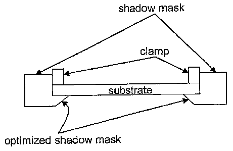
[0030] FIGURE 7 depicts a cross sectional view of one embodiment of an
optimized
perimeter shadow mask.
[0031] FIGURE 8 depicts a photograph illustrating non-uniform film properties
due to edge
effects.
[0032] FIGURE 9 depicts a SERS based detection concept schematic.
[0033] FIGURE 10 depicts a liquid sample dispensing for SERS measurement.
[0034] FIGURE 11 depicts a block diagram of sensor component subsystems.
[0035] FIGURE 12 depicts a timing diagram for proposed chemical and biological
agent
detection system where the complete detection cycle time is 1 minute.
[0036] FIGURE 13 depicts the calculated surface enhanced Raman signal for (a)
toxin and
(b) spore airborne concentrations at various SERS enhancement factors where
the vertical
dotted lines show realistic limit of detection (LOD) requirements and the
stepwise curve in
(b) reflects detection of 1, 2, and 3 spores.
[0037] FIGURE 14 depicts the calculated probability of error.
CA 02569863 2006-12-07
WO 2006/076040 10 PCT/US2005/020245
DETAILED DESCRIPTION OF THE INVENTION
[0038] Before explaining at least one embodiment of the invention in detail,
it is to be
understood that the invention is not limited in its application to the details
of construction and
the arrangement of the components set forth in the following description or
illustrated in the
drawings. The invention is capable of other embodiments or of being practiced
or carried
out in various ways. Also, it is to be understood that the phraseology and
terminology
employed herein is for purpose of description and should not be regarded as
limiting.
[0039] The present invention is useful for many chemical or biological
detection and sensor
applications that require rapid detection. The present invention is a chemical
and biological
detection platform based upon surface enhanced Raman spectroscopy (SERS), a
molecular
detection technique that has been made ultrasensitive. The technological
breakthrough that
has enabled the realization of SERS as an ultrasensitive chemical and
biological detection
method for the presently disclosed and claimed applications has been the
development of
SERS substrates exhibiting extremely high enhancement-factors as described
herein. The
system incorporates SERS substrates that amplify the Raman signal by at least
8 orders of
magnitude and, in some instances, 11 orders of magnitude. These substrates
allow the
system to produce vibrational spectra of analytes, enabling detection and
identification at the
single spore or attogram (10-1$ g) level for toxins and chemical agents.
[0040] The fabrication methodology of the presently disclosed and claimed
invention yields
SERS substrates that produce highly reproducible spectra both at various
positions on a
single substrate and for same samples on different identically prepared
substrates. By
controlling the morphology of the substrates on the nanoscale level, molecular
specificity can
be incorporated into the system, allowing for the selective amplification of
targeted analytes.
Controllable molecular specificity allows the detection of and identification
of target chemical
and biological agents in the presence of high concentrations of interferents
and background
clutter. Since the enhancement of the signal is so great, use of relatively
inexpensive low
performance optical components in the system is feasible, making the system
affordable.
[0041] The performance of the present invention for biological warfare agent
stimulant
samples is shown in Figure 1. For comparison, spectra collected from Live Oak
pollen
single spore, Bacillus thuringiensis single spore, Bacillus cereus single
spore, Bacillus
subtilis single spore, and a single human enteric coronavirus[92] are shown.
The samples
were suspended in water and drop cast onto the substrates prior to analysis.
The spectra
were digitally filtered and the fluorescent background was subtracted. The
spectra show the
high level of information contained in Raman spectra of biological materials
that is essential
for differentiation and identification. Peak heights of up to 1000 cps were
achieved and
signals were integrated for 100 seconds. A low incident laser power of 2.5 mW
at 632.8 nm
CA 02569863 2006-12-07
WO 2006/076040 11 PCT/US2005/020245
was used. The spectral signal to noise ratio (SNR) values range from 10 in the
"fingerprint"
region (800-1750 cm"') to over 39 at the major peaks.
[0042] Since the spectral features in the spectra in Figure 1 are broad, a low
spectral
resolution, high optical throughput miniature spectrometer can be used to
collect the SERS
spectra. An examination of the spectral region of 1500 to 1750 cm-' shows that
this region is
unique to all 5 spectra. Although the peaks in this region for Bacillus
subtilis and the
coronavirus are quite similar, the peak shapes at 2800 to 3100 cm-' are quite
different.
Thus, the overall shape of the spectrum will be used to identify the presence
of bacteria in
the sample and features unique to individual species can be used to identify a
particular
chemical or biological agent. For example, a robust pattern recognition
processing algorithm
incorporating Ward's algorithm for cluster analysis[2] can easily deconvolute
the traces
shown in Figure 1, compare the deconvoluted spectra to a spectral library
database, and
identify bacteria present in the sample. Cluster analysis of vibrational
spectra has not only
been shown to be capable of differentiating between different bacteria in
samples, but has
also been shown to be capable of differentiating between individual strains of
a single
bacteria. This capability is described in detail below.
[0043] A serious and current limitation of many biological agent detection
systems is the
inabiliy to discriminate between live and dead biomaterials. Encouraging SERS
results
regarding this limitation are shown in Figure 2. Spectra were collected on
live Bacillus
thuringiensis spore samples following heating to 100 C, 150 C, 200 C, and
300 C. The
spectra show that compared to the live spore spectrum, both the fluorescent
and Raman
signals decreases upon heating to 100 C. Additional heating to 150 C further
reduces the
fluorescence and Raman intensity. Heating to 200 C decreases the fluorescence
further
and the Raman spectrum is no longer observed. Finally, heating to 300 C
decomposes the
biomaterial and a spectrum characteristic of carbon is observed.
[0044] In Figure 3, the versatility of the presently disclosed and claimed
invention is shown
by producing strong spectra for highly complex biological samples, whole urine
and whole
blood. These spectra were collected similarly to those in Figure 1,
integrating over 40
seconds. No sample preparation was performed on these materials except for
drop casting
them onto the substrates. The samples were allowed to dry at room temperature.
These
samples demonstrate that for even highly complex mixtures of biological
samples, a large
amount of spectral information may be obtained to allow the post measurement
processing
algorithms to effectively extract out component spectra. These component
spectra can then
be used to quantify and identify numerous materials in the sample mixture.
[0045] A major advance in performance achieved with the present invention is
reproducibility in both enhancement factor and sample application to the
substrate. In Figure
4, SERS spectra are shown demonstrating this reproducibility. The spectra were
collected
CA 02569863 2006-12-07
WO 2006/076040 12 PCT/US2005/020245
from a drop cast sample of 1.Ox10-6 molar R6G where half of the sample was on
the SERS
surface and half was not, as illustrated in Figure 4. Spectra were collected
at equally spaced
positions as the R6G was sampled over a 2.0 mm distance (see sample line in
Figure 4)
from a region where the sample was not on the SERS surface, to a region where
the sample
was on the SERS surface. Clearly, spectra collected off the SERS surface show
no Raman
features whereas the spectra collected on the SERS surface are highly enhanced
and
exhibit excellent constancy in intensity, i.e. reproducibility. Each spectrum
was collected
using only 2.5 mW of incident laser power at 632.8 nm and was integrated for
only I second.
In addition to this demonstration of reproducibility at different positions on
a single substrate,
similar levels of reproducibility have also been demonstrated on different
substrates.
[0046] The substrates resulting from the present invention are not only
fabricated by an
inexpensive process that is scaleable to high volume production levels, but
their
performance demonstrates unprecedented levels of signal reproducibility and
high SERS
enhancement. The data in Figures 1-4 show the wide versatility of the present
invention to
reproducibly amplify the Raman signal of a diverse range of analytes, both
biological and
chemical.
[0047] The extreme sensitivity of the present invention is depicted in Figure
5, where SERS
spectra are shown from substrates exposed to the vapor of trinitrotoluene
(TNT), a common
explosive material. A 2 ml vial with cap removed containing a 10 microgram
piece of TNT
was placed in a polycarbonate 4 inch by 4 inch petri dish together with a
SERS'substrate.
The SERS substrate consisted of a SERS film deposited onto the surface of a
standard
glass microscope slide. The petri dish was closed, allowing the TNT to
saturate the
enclosed air inside the petri dish. The spectra in Figure 5 show that
measurable SERS
signals were obtained for exposures to the TNT vapor in 1 hour and larger
signals were
obtained in 3 hours. The only source of TNT available to the SERS substrate
was exposure
to the TNT vapor released from the TNT piece. It is noteworthy that a small
SERS signal
was observed in 5 minutes by merely handling a SERS substrate in the vicinity
of the work
area near the open vial of TNT. These spectra show the potential of the SERS
substrates in
an explosive vapor sensor application.
SERS SUBSTRATE PRODUCTION
[0048] The fabrication of SERS substrates in one embodiment of the presently
disclosed
and claimed invention involves preparing a underlying substrate material,
performing the
deposition, possibly performing a post deposition treatment, and verifying the
substrate
performance. The single most important parameter of performance for SERS
substrates is
reproducibility of high signal amplification both at all points on the surface
and on different
substrates prepared similarly.
SERS Substrate Design
CA 02569863 2006-12-07
WO 2006/076040 13 PCT/US2005/020245
[0049] Initially, a material must be chosen on which to deposit the SERS
amplifying surface.
The role of the substrate material is primarily to provide a support for the
film, although the
optical properties of the material will affect so some extent the recipe for
optimizing the
amplifying SERS film.
[0050] A design of experiments (DOE) is then constructed and executed to
define the
deposition parameter space and quantify the effect of each parameter on the
SERS
amplification and reproducibility of the film. Experimental designs are
statistically robust
methods for quantifying the effects of process parameters on a product with
the minimum
number of experimental runs.[93] Deposition parameters such as mask design,
substrate
temperature, deposition rate, SERS film thickness, post deposition annealing
time and
temperature, etc. can be included in the film deposition parameters to be
optimized in the
DOE. Optimization of the deposition parameters for a given analyte is achieved
by
performing SERS measurements on identically prepared samples applied to each
of the
SERS films produced in the DOE.
[0051] Thus, an effective approach to evaluating thermal evaporation for
producing SERS
tunable films is to perform a DOE whereby a specific number of depositions are
performed at
prescribed parameter value combinations to yield the most information about
the process
with the minimum number of experimental runs. This approach is commonly used
in the
industry to efficiently evaluate the effect of control parameters on a
process. As a result of
this optimization effort, the thermal evaporation process is capable of
producing metal island
films whereby the SERS of the film could be tuned throughout the visible and
into the near
infrared regions of the electromagnetic spectrum. For example, films can be
produced with
surface plasmon resonance wavelengths within 1 nm of design desired
wavelengths.
[0052] As an example of the DOE process, we used a 3-factor Box-Behnken DOE as
a
thermal evaporator that prescribed 15 depositions at specific parameter
setting combinations
(see e.g. R. Gupta, M.J. Dyer, and W.A. Weimer, J. Appi. Phys., 92, 5264
(2002)). The '
three DOE factors (or deposition parameters) we chose to evaluate were
substrate
temperature (Ts), deposition rate (Rd), and film thickness (Tf ) and their
ranges were 31-
120 C, 0.3-1.2 A/s, and 10-30 A respectively. The DOE called for 3 of the 15
runs to be
replicate runs with parameters set at their mid points, Ts = 75.5 C, Rd =
0.75 A/s, and Tf =
30 A. The exact sequence of 15 depositions to produce the gold films
prescribed by the
DOE is shown in Table A. Each film was deposited over a 11.4 mm diameter on
18.0 mm
diameter 0.15 mm thick circular borosilicate glass cover slips (from Fisher
Scientific). Also
shown in Table A are measured SPRW values for each film derived from
extinction spectra
shown in Figure 6A. For each spectrum an SPRW value was assigned to the
wavelength
corresponding to the extinction maximum. The calculated SPRW values in Table A
were
CA 02569863 2006-12-07
WO 2006/076040 14 PCT/US2005/020245
obtained from an empirical equation generated from the DOE statistical
analysis as
described herein below.
Table A. Gold Film Deposition Matrix.
Substrate Film SPRW SPRW
Temperature Deposition Thickness Calculated Measured Difference
Sample ( C) Rate (A/s) (A) (nm) (nm) (nm)
1 75.5 0.75 30 615 616 -0.59
2 75.5 0.75 30 615 620 -4.59
3 75.5 1.2 10 563 569 -5.87
4 75.5 1.2 50 650 650 -0.15
31 0.75 50 710 707 2.60
6 120 0.3 30 588 586 2.08
7 31 0.75 10 582 574 7.88
8 75.5 0.3 10 564 564 0.38
9 120 0.75 50 599 607 -7.65
31 1.2 30 656 658 -1.92
11 31 0.3 30 666 674 -8.17
12 75.5 0.3 50 650 644 6.10
13 120 0.75 10 555 557 -2.37
14 120 1.2 30 596 588 8.33
75.5 0.75 30 615 610 5.41
[0053] The tunability in extinction maxima and corresponding SPRW values is
clearly
illustrated in the spectra shown in Figure 6A. An examination of the
extinction spectra in
Figure 6B indicates that the useful range of tunability for these films is
limited to values
greater than 475 nm. Below this limit, absorption due to d electron
transitions dominates the
optical properties of gold. Figure 6B shows that nearly identical spectra were
obtained from
the three identical runs producing films 1, 2, and 15 in Table A. The
reproducibility of the
process in Figure 6B is excellent.
CA 02569863 2006-12-07
WO 2006/076040 15 PCT/US2005/020245
ASp~ =575-0.839TS -43.32Rd +5.68Tf +0.00396T2 +0.225TsRd -0.0233TSTf +16.5Rd
(2)
+0.0278RdTf -0.0297Tf
[0054] The greatest process design challenge to produce SPRW tunable films is
demonstrating an ability to produce films with reproducibility and
predetermined SPRW
values. Therefore, one of the most important results obtained from the DOE
analysis is the
empirical predictive equation produced by fitting Equation 2 to the measured
SPRW values
listed in Table A. In order to demonstrate the predictive capability of
Equation 2 and the
level of control of the process, a target SPRW for a gold film was chosen to
be 640 nm.
According to Equation 2, the appropriate deposition parameters to obtain this
target SPRW
are TS 35 C, Rd=0.7 A/s, and Tf =26 A. The actual SPRW obtained from a gold
film grown
using these deposition parameters was 641 nm, a difference of only 1 nm. The
predictive
ability of Equation 2 and the control of the process were, therefore,
demonstrated to be
excellent.
SERS Substrate Fabrication
[0055] SERS substrates are fabricated by coating a substrate material with a
film prescribed
by the results obtained from the DOE substrate design process. The deposition
process
involves cleaning the substrate material, mounting the substrate materials
into a vapor
deposition apparatus such as a thermal evaporator, performing the deposition,
performing
post deposition processes such as annealing, and characterization of the SERS
substrate.
[0056] Cleaning. Regardless of the substrate material chosen upon which to
deposit the
SERS amplifying film, the surfaces of the materials must be free of
contaminants to ensure
uniform deposition and adequate adhesion of the SERS film. Cleaning typically
involves
soaking or sonicating the substrate material in a series of cleaning
solutions. In one
embodiment of the cleaning procedure, glass substrate materials are sonicated
for 10
minutes in order in each of the following solutions, dilute detergent in
distilled water, distilled
water, and acetone with drying under flowing nitrogen between each sonication.
Many other
cleaning solutions (such as aqua regia, various organic solvents, acids,
bases, etc.) and
procedures (such as heated sonication, irradiation, and soaking in caustic
media, etc.) can
be envisioned by one skilled in the art depending upon the substrate material
and the
condition of the material's surface.
[0057] Mounting. The cleaned substrate materials are next mounted in an
apparatus
designed to control deposition parameters sufficiently to follow the
prescribed by the design
DOE. The presently disclosed and claimed invention includes a mounting method
to ensure
uniform deposition and maximize the useful area of a substrate by prearranging
a perimeter
CA 02569863 2006-12-07
WO 2006/076040 16 PCT/US2005/020245
shadow mask onto the surface of the substrate during deposition. The mask will
minimize
edge effects that result in non-uniform film properties that occur in vapor
deposition in the
absence of a perimeter mask. Such a mask, similar to that illustrated in
Figure 7, would
ensure uniform deposition conditions (such as vapor flux, temperature,
exposure angle, etc.)
over the entire exposed area of the substrate to produce a uniform film over a
large area.
[0058] Figure 8 illustrates the non-uniformity of film properties that results
from edge effects.
The substrate is a 1 inch by 3 inch glass microscope slide coated with a gold
island film that
was clamped in place on both ends. The end clamps also served as shadow masks.
No
constraints or masking was used along the long edge of the slide.
[0059] Figure 8 shows that the film is blue-green in color near the edges of
the film while it is
pink in color near the center of the film. Clearly, this film is not uniform.
The central region is
pink in color due to larger island sizes and larger inter-island spacing. The
outer regions are
blue-green because the islands are smaller in diameter and spaced closer
together. The
primary causes of the non-uniform film are due to non-uniform local deposition
conditions
very near the substrate across the substrate surface. The film near the edges
of either
clamped end is pink nearly up to the clamp position, particularly on the left
edge of the film.
The blue-green film region at the clamped edges is quite narrow and could be
eliminated
with an optimized mask geometry. Along the long edges of the film where no
mask was
employed, the blue-green region of the film extends from the substrate edge to
nearly a
fourth of the width of the film. Clearly, where no shadow mask is used,
significantly non-
uniform films can be expected and that non-uniformity can extend into the area
of the film a
significant distance. The edge effects illustrated in Figure 8 are even more
significant (i.e.
extend farther into the film area) when larger area films are deposited on
larger area
substrate materials. The edge effects are also worse for unmasked films when
deposition
cycle times are reduced in order to mass produce large area films.
[0060] For large area films, it is absolutely essential that the films are
uniform to ensure a
constant SERS enhancement factor for an analyte placed at any position on the
film. For a
SERS based sensor, therefore, extremely high uniformity of the film and
maximal film
coverage are critical. Both of these requirements necessitate the use of an
optimized
perimeter shadow mask. Variations in the island geometry and spacing produce
variations
in SERS signal strength. Such variations produce, therefore, non-quantifiable
measurements. Quantitative measurements, traceable to reliable standards, are
absolutely
necessary for the films to be used in a SERS based sensor.
[0061] Incorporation of a perimeter shadow mask of high thermal mass and
conductivity that
is suitable for high vacuum service, such as stainless steel, uniform heating
of the substrate
during deposition is achieved by integrating the mask into the substrate
heating design.
Actively heating at the edge of the substrate ensures uniform temperature of
the substrate
CA 02569863 2006-12-07
WO 2006/076040 17 PCT/US2005/020245
during deposition and post deposition annealing processing by counteracting
thermal energy
losses due to convection, conduction, and emission. In order to be effective,
optimal thermal
contact between the mask and substrate must be achieved so the mask is
attached to and in
physical contact with the exposed surface of the substrate to ensure efficient
thermal energy
flow between the mask and the substrate.
[0062] A perimeter shadow mask enables the formation of registration marks
onto the
substrate that may subsequently be used to ensure optimal optical alignment
and substrate
positioning during use in an autonomous SERS sensor application or device.
[0063] Deposition. The presently disclosed and claimed invention also includes
a method
for the formation of the film onto the surface of the substrate material. The
film formation
must be controlled so that the deposition parameters called for from the
design DOE are
maintained within acceptable tolerances. In one embodiment of the presently
disclosed and
claimed invention, the design DOE calls for precise control of deposition
rate, substrate
temperature, and SERS film thickness to constant values in a thermal
evaporator. The
deposition rate and film thickness are monitored using an oscillating crystal
sensor and the
substrate temperature is monitored using a thermocouple in contact with the
substrate
material or other suitable device such as an infrared radiation thermometer.
[0064] The deposition apparatus may be a thermal evaporator. In this case,
metal vapor is
formed in a vacuum chamber by heating a refractory metal, such as tungsten,
vessel
containing the metal to be deposited such as gold. Electrical current is
passed through the
boat, causing the boat to heat to high temperatures by resistive heating.
Deposition
parameters may be held constant or varied in a controlled manner during
deposition. When
the metal in the boat reaches a high enough temperature, the metal emits vapor
consisting
of the metal in the gas phase. If the vapor is allowed to contact a substrate,
held at a much
lower temperature, the vapor condenses on the substrate surface, allowing the
accumulation
of a film of the metal on the substrate surface. Numerous other methods for
vapor
depositing metal films are commercially available, such as laser ablation,
electron beam
evaporation, plasma assisted chemical vapor deposition, etc. and could be used
in another
embodiment of the presently disclosed and claimed invention.
[0065] Measurement Method. The presently disclosed and claimed invention
further
includes a method for optimal production of surface enhanced Raman spectra
from
biological materials. This invention incorporates the counterintuitive process
of avoiding
tuning the local surface plasmon resonance wavelength to between the laser and
Raman
shifted wavelengths since doing so produces deleterious effects for biological
samples.
Tuning the surface plasmon to between the laser and Raman shifted wavelengths
to
produce the maximum electric field adjacent to the outer surface of the
substrate acts to
denature biological material and results in the observation of enormous Raman
signals due
CA 02569863 2006-12-07
WO 2006/076040 18 PCT/US2005/020245
to carbon. These carbon signals result from the denaturation process. The
electric fields
associated with optimal surface plasmon resonance, therefore, are not desired
for biological
samples. In fact, for biological and other fragile materials, there does not
exist a "desired"
wavelength for the local surface plasmon resonance.
[0066] The presently disclosed and claimed invention includes a method to tune
the surface
plasmon resonance to any of a range of wavelengths significantly longer than
that
conventionally considered "optimal." In other words, a suitable substrate for
biological
samples is one where the local surface plasmon resonance is tuned to any
number of
wavelengths that are longer than the Raman shifted wavelengths. So the
generally
accepted prior art "rule" for optimal tuning that prescribes to place the
local surface plasmon
resonance between the laser and Raman scattered wavelengths does not
universally apply
to biological materials.
[0067] Apparatus. Another embodiment of the presently disclosed and claimed
invention
uses a high volume air sampling system. This system is designed to collect and
concentrate
a measurable amount of analyte in a liquid and deliver an aliquot of the
solution onto a
SERS substrate surface, preferably in less than one minute. In one embodiment
of the
presently disclosed and claimed invention, the air sampling system permits the
sampling of
an air steam from a heating, ventilation, and air conditioning (HVAC) duct,
and subsequent
collection of aspirated particles. The air sampling system may include the
installation of an
in-line fluorescence sensor in the sampling conduit to permit detection of the
presence of
biological species and possible automated triggering of liquid sample transfer
to a'detection
system. The system may be optimized with respect to the response time of air
sampler by
minimizing the time from initial introduction of sample to the registration of
a detection
response. The system may be further optimized with respect to minimizing the
time
necessary for concentration of analytes in the liquid phase which in effect
minimizes the
overall sampling collection time.
[0068] The present invention may incorporate a liquid handling system
consisting of
computer-controlled valves, a peristaltic pump, and a syringe/dispensing
apparatus that may
be configured to deliver highly-reproducible aliquots of extracted liquid
phase onto the SERS
substrate. In addition, the system may incorporate compact micro-positioning
hardware that
is able to facilitate precise movement of the sample dispenser and substrate
turntable to
optimize sample positioning with respect to the incident laser beam during
sample
deposition, evaporation, and SERS measurement processes. The air sampling and
liquid
delivery components may, in an alternate embodiment, be integrated to perform
fully
automated under computer control using process software that will allow
autonomous
operation of the SERS based sensor. Particularly, control of micro-positioning
hardware and
CA 02569863 2006-12-07
WO 2006/076040 19 PCT/US2005/020245
timing of individual actions may be achieved that include the duration of air
sampling prior to
liquid sample transfer, and the deposition of the sample droplets.
[0069] Self testing, optimization and calibration may be incorporated into the
sensor to
ensure accurate and reproducible measurements over long periods of time.
Predeposited
calibration samples may be place onto the surface of the SERS surface which
may be
periodically measured to achieve this elaborate self test. The system can be
programmed to
report its condition or adjust itself by taking corrective action such as
undergoing an *
automated realignment process. Corrective action may be taken to maintain
optimal
performance with respect to sample reproducibility and execution within the
timeframe
allowable within the prescribed collection and measurement cycle. Contingent
upon
successful self testing of the entire sensor system, the operation of each
individual
component may be optimized to achieve maximum time efficiency, and sampling
repeatability.
[0070] Various commercial designs for wetted-wall cyclone air sampling systems
may be
used in the SERS based sensor to optimize the collection efficiency, ease of
operation, and
compatibility with the specific requirements of the intended application.
[0071] The SERS substrates may be further enhanced by optimizing the process
for
fabrication of SERS substrates for the detection of specific analytes. Such
optimization may
include modification of the SERS film itself, modification of the composition,
shape, and
function of the substrate material supporting the SERS film. Optimization of
the SERS
substrate material function and other sensor functions may include turntable
rotation speed
and pause duration, solvent evaporation processing, heating and SERS laser
powers,
optical alignment, and spectrometer operation.
[0072] The software used for spectral analysis and analyte identification may
be optimized
by providing a model of the SERS sensor system that will enable the prediction
of
performance and perform post-measurement analysis on data generated by the
SERS
detector to identify and quantify the concentration of analytes very rapidly.
Further
optimization of the system software may include the incorporation of an
analyte fingerprint
algorithm to statistically match the measured SERS spectrum to the a spectrum
in an
analyte database. Also, clustering algorithms can be implemented, such as the
well-tested
Ward's algorithm.
[0073] A schematic representation of one embodiment of the apparatus of the
presently
disclosed and claimed invention is shown in Figures 9 and 10. Briefly,
airborne material is
captured in a liquid to form a sample solution that is representative of the
air concentration.
An aliquot of this solution is applied to the surface of a turntable coated
with a SERS film
produced according to the methods disclosed herein. The turntable is then
rotated to
translate the sample to the measurement beam for detection and identification
of the
CA 02569863 2006-12-07
WO 2006/076040 20 PCT/US2005/020245
sample. This controlled application of the liquid sample concentrates the
analyte to a small
spot suitable for SERS measurement.
[0074] A novel aspect of the sensor system concept is the concentration of
microliter scale
liquid sample volumes onto extremely small (<100Nm) spots on the SERS
substrate prior to
detection. Ink-jet technology is used to dispense sub nanoliter droplets onto
the SERS
substrate. For example, . The individual
droplets, nominally 50Nm in diameter, will wet out to nominally 100pm spots on
the SERS
substrate. The combination of very high surface area to volume of the small
droplets, plus
the heating of the substrate, causes the droplets to evaporate in a fraction
second. Using
the inherent digital control of the ink-jet processes, subsequent droplets are
applied after
most of the previous drop has evaporated. Extending this process to hundreds
or thousands
of drops, the nonvolatile solids in the microliter scale liquid sample volume
are concentrated
onto a roughly 100Nm spot.
[0075] Below, a performance model for the present invention is described and
the function is
quantified for each of the subsystems in the design: air sampler, sample
applicator, SERS
detection system, and post detection analysis. A block diagram of these
subsystems is
shown in Figure 11 and a timing diagram for the complete detection cycle is
shown in Figure
12.
[0076] Sample "clean-up" can be achieved during fluidic transfer between a
wetted-wall
cyclone sampler and the SERS module by a sequential series of rapid, on-line
processes
that may include separation of particles by size exclusion, selective
partitioning of particles
between aqueous and non-aqueous liquid phases, and mechanical agitation
(sonic). Finally,
a computer-controlled syringe dispenser can be used to inject a microliter
volume of water
into the liquid sample line, upstream from the deposition capillary, to
displace an equal
volume of "cleaned-up" liquid sample into the inkjet dispenser, or
alternatively, a dispensing
capillary. Provisions are to be made for automated purge/flushing of the
sample transfer line
following sample deposition. Following detection, the contents of the liquid
phase could be
automatically transferred to an appropriate receptacle for archiving purposes.
[0077] In order to verify the performance and reliability of the detection
system on a day-to-
day basis, an automated quality assurance (QA) scheme may be implemented. One
such
QA scheme requires the detector to examine a pre-deposited sample or samples
containing
an appropriate reference analyte in a mixture including typical background and
particulate
interferents. The objective is to confirm that the detection signal-to-noise
ratio meets
minimum specifications and that absolute identification can be achieved under
challenging
conditions. Pending the outcome of the QA procedure, the system can proceed
with
autonomous monitoring, or necessary corrective measures can be taken including
modem or
CA 02569863 2006-12-07
WO 2006/076040 21 PCT/US2005/020245
wireless or any other manual, automated or semi-automated communication means
to
initiate remote diagnosis.
[0078] During routine operation of this embodiment of the present invention, 5-
8 ml of liquid
phase containing accumulated aerosols will reside in the wetted-wall cyclone
sampler during
SERS identification of the most recently deposited sample. In the event of a
positive
identification of an analyte such as a biological pathogen, this volume, or
some
representative portion thereof, will be readily available for automated
transfer to an
appropriate receptacle for archiving purposes. In such an instance, the liquid
phase is likely
to contain a sufficient amount of analyte to enable confirmatory and forensic
analyses at a
later date.
[0079] A high velocity virtual impactor is incorporated into the first stage
of the air sampling
system. For example, the MSP Corporation Model 340 HWI high volume virtual
impactor
samples air at 1130 Umin with a cut point of 2.5 m. The second stage of the
air sampler
may also incorporate a wetted-wall cyclone. The wetted-wall cyclone sampler
provides
suction to extract sample stream air from the virtual impactor. Upon
introduction of the
extracted air stream into the wetted-wall cyclone, entrained particles collide
with the thin
liquid film coating the walls of the cyclone and are effectively removed from
the sample air
stream. A small volume (5-8 ml) of liquid continuously circulates through the
cyclone
chamber and accumulates particles from the sample air stream. Following a
remote
command, the liquid phase is transferred to the SERS detection module and the
cyclone cup
is recharged with fresh liquid.
[0080] Ink-jet printing technology can reproducibly dispense spheres of fluid
with diameters
of 15 to 100 m (2 pl to 5 ni) at rates of 0 - 25,000 per second from a single
drop-on-demand
printhead. The deposition is non-contact, data-driven and can dispense a wide
range of
fluids. In a drop-on-demand ink-jet printer, the fluid is maintained at
ambient pressure and a
transducer is used to create a drop only when needed (see Figure 9). The
transducer
creates a volumetric change in the fluid which creates pressure waves. The
pressure waves
travel to the orifice, are converted to fluid velocity, which results in a
drop. being ejected from
the orifice.
[0081] The transducer in demand mode ink-jet systems can be either a structure
that
incorporates piezoelectric materials or a thin film resistor. In the later, a
current is passed
through this resistor, causing the temperature to rise rapidly. The ink in
contact with it is
vaporized, forming a vapor bubble over the resistor. This vapor bubble creates
a volume
displacement in the fluid in a similar manner as the electromechanical action
of a
piezoelectric transducer. Demand mode ink-jet printing systems produce
droplets that are
approximately equal in diameter to the orifice diameter of the droplet
generator. Droplet
generation rates for commercially available demand mode ink-jet systems are
usually in the
CA 02569863 2006-12-07
WO 2006/076040 22 PCT/US2005/020245
4-12 kHz range. Droplets less than 20 pm are used in photographic quality
printers, and
drop diameters up to 120 pm have been demonstrated.
[0082] As a non-contact printing process, the volumetric accuracy of ink-jet
dispensing is not
affected by how the fluid wets a substrate, as is the case when positive
displacement or pin
transfer systems "touch ofP" the fluid onto the substrate during the
dispensing event. In
addition, the fluid source cannot be contaminated by the substrate, as is the
potential during
pin transfer touching. Finally, the ability to free-fly the droplets of fluid
over a millimeter or
more allows fluids to be dispensed into wells or other substrate features
(e.g., features that
are created to control wetting and spreading).
[0083] In general, piezoelectric demand mode technology can be more readily
adapted to
fluid microdispensing applications and it is easier to achieve lower drop
velocities with
piezoelectric demand mode. Piezoelectric demand mode does not create thermal
stress on
the fluid, which decreases the life of both the printhead and fluid.
Piezoelectric demand
mode does not depend on the thermal properties of the fluid to impart acoustic
energy to the
working fluid, adding an additional fluid property consideration to the
problem.
[0084] As shown in Figures 9 and 10, the present detection system will
interface the
microdispenser to the wet walled cyclone air sampler to generate reproducible
sample
deposits on the SERS surface. The sample deposition parameters are optimized
to produce
the highest enhancement of the SERS signal. Laboratory results using
micropipets have
shown that a 5 l drop yields acceptable deposits for SERS measurements,
although the
process is cumbersome. Therefore a 5 l of sample can be deposited with the
microdispenser using multiple (500-1000) drops.
[0085] Fundamental to the detection system, the signal (molecular signature
amplitude)
produced, S(e) (in e), for 180 backscattering geometry and low f number
optics used for
both excitation laser focusing and Raman scatter collection:[94]
S(e ) = (1'D/3 NS, XAD 0 D 7'wrQ) t, (3)
[0086] where PD is the incident laser power density (in photons s'' cm 2), #
is the differential
Raman cross section (in cm2 molecule' sr'), NS, is the number of scatterers
per unit area (in
molecule cm"2) on the SERS surface, AD is the sample area monitored by the
spectrometer
(in cm2), Do is the collection solid angle of the spectrometer at the sample
(in steradians),
T,o, is the transmission of the collection optics (unitiess), Q is the quantum
efficiency of the
detector (in e" per photon), and t is the observation time (in seconds). In
Equation 3, the first
terms in parentheses, PD ,fi, and Ns , are related to the generation of Raman
scattered
photons and the remaining terms describe the detection of those photons.
[0087] Assuming an airborne concentration of Bacillus subtilis spores of 100
spores per liter
ofair,Ca=100L-'.
CA 02569863 2006-12-07
WO 2006/076040 23 PCT/US2005/020245
[0088] The wet walled cyclone sampler is capable of sampling air at a nominal
rate of As =
260 L/min with an efficiency for 1.0 m diameter particles of 50%. Thus, the
spore collection
rate, R, for the cyclone air sampler is given in Equation 4 and is simply the
product of the air
concentration Ca, sampling rate As, and collection efficiency E,,
R, =CQASE, (100j4.33L)0.5=216.5s-1. (4)
[0089] The concentration of captured spores in the recirculating liquid, CS,
is given by
Equation 5. The volume of recirculating liquid in the sampler is VS = 10 ml.
Assuming a
collection time of Ts = 30 s, the concentration in the cyclone liquid is
CS = R,Ts l VS =~ 216.5 ) 30 s I 1 J=649500L* (5)
s 10.01L[0090] The volume of recirculating liquid deposited onto the SERS
surface is Vd =
5.0 l. Therefore, the number of spores collected from the recirculating
liquid and delivered
to the SERS surface in one drop, Ns, is
NS = C.sVdEt [6495oo)(5.OX1O6 L)1.0 = 3.25 spores, (6)
[0091] where Et is the transfer efficiency of the 5.0 l sample from the air
sampler, through
the transfer plumbing, to the SERS surface; a value of 1.0 is assumed.
[0092] Combining formulas 3-5, the number of spores, NS, delivered to the SERS
surface
per sampling event is
Ns = CaAsE,TsEtVd IVS, (7)
where all terms are defined above.
[0093] The shape of a Bacillus subtilis spore may be approximated to be a
prolate spheroid
with a minor axis of 0.75 m and a major axis of 1.25 m.[95] The cross
sectional area of a
single spore, therefore, is A sp =7u(r,r2) = 7.4x10⁻⁹ cmZ. The collected
spores, if close packed
and a fill factor of Ff = 80%, would occupy about ASP = NAsplFf = 3(7.4x10'9
cm2)/0.8 =
2.8x10"$ cm2, nearly filling the 3.14x10"$ cm2 excitation laser beam.
[0094] Here, it is assumed that the 3 spores dropped and evaporated onto the
SERS
surface are close-packed under the Raman laser beam. The 3 spores combine to
an area of
2.2x10"e cmZ. Since the laser beam area is 3.1x10⁻⁸ cm2, perfectly placed
spores will be fully
illuminated by the laser.
[0095] The intensity of stokes shifted Raman scattered radiation, /R, in all
directions is[94]
IR = PD,8 Ns~ , (8)
CA 02569863 2006-12-07
WO 2006/076040 24 PCT/US2005/020245
[0096] where Po is the incident laser power density (in photons s-' cm"z) at
the sample, ~8 is
the differential Raman cross section (in cm2 molecule-' sr'), and Ns, is the
number of
scatterers per unit area (in molecules cm-2). The incident laser power, Po,
for the system is
70 W, and the energy of each photon at 632.8 nm is EP = hc/~, where h is
Planck's
constant (6.626x10⁻³⁴ J s), c is the speed of light (3.0x10⁸ m/s), and ~ is
the laser
wavelength (632.8x10⁻⁹ m). It is assumed that the incident laser radiation
will excite Raman
scattering over 20 bands. Therefore, the power density available for any given
band will be
5% of the overall incident power:
0.05P 0.05 (70x10'6 J/ s) zo i -2
PD = _ =3.5x10 photons s' cm . (9)
ALEp 3.14x10⁻⁸cmz 3.14x10'19J/ photon
[0097] The Bacillus subtilis spore surface is composed of about 27
proteins.[96] Since they
are weak scatterers, a typical value for the Raman cross section, fl, of amino
acids is j6 = 10"
30 cm 2 sr' molecule'. From above, the area occupied by Ns = 3 spores is A'sP
= NAsP =
3(7.4x10⁻⁹ cmz) = 2.2x10"e cm2. Assuming the area of a single amino acid is
Aaa = 200 A 2 (or
2.0x10⁻¹⁴ cmz), the number of amino acids contained in the area of the 3
spores is Naa =
A"splAaa = 2.2x10;8 cmz/2.0x10-14 cm2 = 1.1x10⁶. It is further assumed that
100% of the
1.1x10⁶ surface amino acids are in contact with the SERS surface. The laser
beam diameter
AL at the surface is used to calculate surface density of scatterers NS,, thus
6
N_ NQa _ 1.1x10 = 3.5x10¹³ molecule cm-z,
S AL 3.14x10-g cm z
(10)
[0098] Combining results from Equations 9 and 10 and the value for,l3 into
Equation 8 yields
In - PD,8 Ns 3.5x10²⁰ Photons 10'30 cm2 3.5x10¹³ molecule 12,250Photons
s cm2 sr molecule cmz s sr cm2
(11)
[0099] Recalling from Equation 3 that S(e) = IR(Ao.rloTc,,iQ)t, the remaining
terms related to
the collection of Raman scattered light are evaluated, where Ao = 3.1x10-e
cm2, ,flo = 0.4 sr,
T,o, = 50%, Q = 80%:[94]
12'250photons 0.8 e6.1x105 eS(e) (3.1x1o8cm2Xo.4srXo.5 t= t.(12
s sr cm photon s
z
)
The signal to noise ratio is calculated as follows:[94]
s Nsc vz
SNR = liz (PDADS2TC tlQt) ,
(~scNsc +~BDB)
(13)
CA 02569863 2006-12-07
WO 2006/076040 25 PCT/US2005/020245
[0100] where 6S,NS, is the cross section density product for the signal and
PBN8 is the cross
section density product for the detector background. OL3NB includes
contributions to the
detector background signal from all sources such as shot noise, Johnson noise,
dark count,
flicker noise, and readout noise. For state-of-the-art CCD detectors, j8BNB is
roughly 1 e per
second.
[0101] Figure 13 shows Raman signals calculated for various airborne spore and
toxin
concentrations using performance values typical for a commercial cyclone wet
walled
sampler and a well designed Raman spectrometer. These results show that if a
SERS
enhancement factor of 1010 or greater is achieved, the system will have
sufficient sensitivity
to meet and exceed limits of detection requirements for bacteria and toxins of
100 spores
per liter of air and 0.05 ng per liter of air, respectively. The results also
show that a 1010
SERS enhancement factor produces a signal strong enough to allow for the
detection cycle
time of 1 minute or less to be achieved for both spores and toxins.
[0102] The false alarm rate for the system can be estimated using the well
known threshold
effect, a statistical analysis method developed in the communications industry
for
determining the error rate of digital signals.[97] The analogy of this effect
to this analysis is
straightforward, since it is desirable to establish the statistical
significance of the detector
producing a signal above or below a predetermined threshold (set to the threat
level). Thus,
determining a negative alarm condition (signal below threat level) or positive
alarm condition
(signal above threat level) is identical for binary digital signals
representing a zero (below
threshold) or a one (above threshold) respectively.
[0103] For signals containing Gaussian distributed noise, the probability of
error in above or
below threshold signals is:
P. =1 2 1- erf 2~6 , where erf (x) _2 f xe-vZ dy
(14)
[0104] and where Pe is the probability of error, A is the maximum signal
amplitude, Q is the
signal standard deviation, and erf is the error function. It is assumed in
Equation 14 that the
threshold is set to A12. For a prescribed false alarm rate of 10"2, Equation
14 requires a
signal to noise ratio, SNR = A/Q= 4.8, as shown in Figure 14. Clearly, the
data in Figure 1
exceeds this signal to noise ratio. The standard deviation term, or, in
Equation 14 contains
contributions from all subsystems, including the air sampler, sample
applicator, SERS
detector, and post detection identification analyzer.
[0105] A complete propagation of error analysis of the subsystems can be
performed to fully
quantify contributions to the system uncertainty due to the subsystems with
particular focus
on the contribution due to uncertainty in analyte identification. In addition,
a model can be
CA 02569863 2006-12-07
WO 2006/076040 26 PCT/US2005/020245
derived to calculate the contribution to a due to spectral clutter. Finally, a
model to calculate
the probability of detection in the form of a Receiver Operating
Characteristic (ROC) curve
can be developed. Similar ROC curves can also be generated using experimental
data to
verify the model.
[0106] Following air sampling and spectral acquisition, the rapid and reliable
interpretation of
the collected Raman signal is the final and perhaps the most crucial step in
detecting a
potential threat from an aerosol contagion. The interpretation of Raman
spectra from
complex media is challenging due to the high density of states from the
immense number of
individual oscillators in the sample, which coalesce into a spectrum composed
of relatively
few bands. A simple group frequency/structural class analysis is not
applicable to such
systems. In the presently disclosed and claimed invention, the interpretation
of the Raman
signal involves a three stage strategy following acquisition of the spectral
data: (1)
fingerprinting, (2) cluster analysis and, (3) threat evaluation.
[0107] To reduce the data set to a manageable size and in order to identify
key aspects, the
Raman spectra can be processed into characteristic fingerprints of equal or
lower
dimensionality, without loss of critical information. The primary fingerprint
may be defined by
the input spectral data, typically consisting of approximately 2000 data
points over the
spectral region 150 to 4000 cm-'. The raw data can be normalized and the first-
and second-
derivative spectra are computed using a 9-pt technique, to allow the
extraction of precise
wavenumbers and integrated band intensities, minimizing concern for
unavoidable baseline
shifts. Secondary fingerprints, which are substantially more compact than the
primary, can
be derived from band analysis (frequency and intensity), region analysis
(number of bands
and total integrated intensity), local mode assignment (key vibration
identification), statistical
correlation analysis (PCA) and/or a combination of these.
[0108] A critical requirement for reliable correlation of analyte signal with
known warfare
agents is the development of a spectral library or database. Creation of a
database,
containing the fingerprints of analytes of interest is the first priority in
working to develop the
presence of analyte assessment algorithms.
Table B. Raman Spectral Wavenumber Region Assignments.
Region (cm-') Assignment
400 - 900 True "Fingerprint Region" (variable, highly specific)
900 -1200 Polysaccharide Region (cell surface markers)
1200 - 1550 Proteins, Fatty Acids and Phosphates
1550-1800 Mixed Region
CA 02569863 2006-12-07
WO 2006/076040 27 PCT/US2005/020245
1800 - 3600 Double, Triple Bonds and Hydrogen Stretches
[0109] Cluster analysis is the automated categorization of data into
algorithmically defined
"clusters" based on similarity metrics. In the current context, it refers to
the systematic
comparison of the analyte fingerprint to entries in the database for the
purpose of
determining the presence of an analyte of interest. The analysis relies on the
defined
measures of closeness in comparing fingerprint signatures. Analysis is carried
out on the
fingerprints considering five spectral regions 400 to 900, 900 to 1200, 1200
to 1550, 1550 to
1800 and 1800 to 3600 cm-'. These regions naturally suggest themselves since
they
correspond to scattering due to vibrational modes associated as indicated in
Table B.
[0110] Similarity between fingerprints can be evaluated through a number of
descriptors,
including: Euclidian distance, maximum difference and projected length; along
with an
agglomerative clustering approach. Several clustering algorithms will be
assessed, starting
with the well-established Ward's algorithm, which seeks to minimize the total
sum of squared
deviations between analyte and database spectra.
[0111] The presently disclosed and claimed invention relates to a method to
optimize
deposition parameters to produce the highest SERS enhancement factor for
specific Raman
lines of a specific target molecule. This method involves producing a series
of films
according to a design of experiments (DOE) protocol whereby vapor deposition
fabrication
parameters (such as substrate temperature, deposition rate, film mass
thickness, chamber
pressure, and post deposition annealing) are set within predetermined
parameter ranges
and with specific combinations specified by the DOE. The SERS enhancement
factor of
each film is measured and a DOE statistical analysis is thereafter performed
to quantify the
effect of each deposition parameter on enhancement factor. This analysis
quantifies the
sensitivity and magnitude of the effect from which the optimum deposition
parameters are
obtained. An empirical predictive equation is produced from such a DOE
statistical analysis
that allows the deposition parameters to be set to produce a predetermined
enhancement
factor for a specific molecule.
[0112] In an alternative embodiment, the presently disclosed and claimed
invention includes
a method to produce a metal film having optimal surface enhancing properties
for specific
regions of the Raman spectrum. Often, a specific region of a Raman spectrum is
of
particular interest. It is useful, therefore, to enhance the SERS spectrum
over a specific
region of the spectrum. The spectral range (or width) over which the metal
island films can
produce a high SERS enhancing effect is limited, although, this range can be
controlled to
occur over a predetermined spectral region. This method involves producing a
series of
films according to a design of experiments (DOE) protocol whereby vapor
deposition
fabrication parameters (such as substrate temperature, deposition rate, film
mass thickness,
CA 02569863 2006-12-07
WO 2006/076040 28 -PCT/US2005/020245
chamber pressure, and post deposition annealing) are set within predetermined
parameter
ranges and with specific combinations specified by the DOE. The spectral
region and width
of the SERS enhancement factor of each film is measured and a DOE statistical
analysis is
performed to quantify the effect of each deposition parameter on the spectral
region and
width of the SERS enhancement factor. The analysis quantified the sensitivity
and
magnitude of the effect from which the optimum deposition parameters are
thereafter
obtained. An empirical predictive equation is produced from such a DOE
statistical analysis
that allows the deposition parameters to be set to produce a film exhibiting
maximized SERS
enhancement over a predetermined spectral region of the SERS spectrum.
[0113] The presently disclosed and claimed invention further includes a method
to deposit
film with high SERS enhancement factor and increased film environmental
durability. This
method deposits a film with the SPRW to the red of laser line, then the film
is heated in
vacuum chamber immediately following deposition to blue shift the SPRW to
optimum value.
The procedure achieves a high SERS enhancement factor and increases film
environmental
durability due to annealing the metal islands and inducing them to form highly
stable shapes.
The post deposition heating causes a decrease in the metal island diameters
along with a
concurrent increase in the island heights. Both of these changes in island
geometry produce
a blue shift in the SPRW.
[0114] The presently disclosed and claimed invention also includes a method to
treat
substrate to adsorb molecules in gaps between gold islands on film. This
method applies a
coating to the substrate that exhibits a high affinity for a target analyte
molecule prior to
depositing gold. Following gold deposition, target molecules will thereafter
have an affinity to
adsorb in gaps between gold islands on film following application of the
sample to the SERS
film. Capturing the analyte molecules in the gaps between the gold islands
maximizes the
SERS enhancement factor for those molecules because it is believed that the
electric field
associated with the surface plasmon resonance is greatest maximum between the
islands.
Molecules captured such that they are engulfed by this maximum electric field
will maximize
the SERS spectrum produced.
[0115] In yet another aspect, the presently disclosed and claimed invention
includes a
method to deposit gold, silver, or other substance simultaneously or
sequentially on a
substrate. This method utilizes two or more vapor sources operating
simultaneously, or in
series, to produce islands comprising shell structures, amalgams, or mixtures
onto the
surface of various supporting substrate materials including, but not limited
to glass, liquid
crystal, ceramics, semiconductors, semimetals, polymers, fibers, composites,
nanomaterials,
and mixtures and/or combinations thereof. In one embodiment, silver islands
are first
deposited then followed with gold to produce gold coated silver islands. This
method allows
CA 02569863 2006-12-07
WO 2006/076040 29 PCT/US2005/020245
the optimization of metal island films to SERS systems using near infrared and
longer
wavelength laser excitation.
[0116] In yet another alternate embodiment, the presently disclosed and
claimed invention
includes a method to actively vary deposition parameters during deposition of
a metal on a
substrate. This method involves producing a series of films according to a
design of
experiments (DOE) protocol whereby vapor deposition fabrication parameters
(such as
substrate temperature, deposition rate, film mass thickness, chamber pressure,
and post
deposition annealing) are varied during deposition within predetermined
parameter ranges
and with specific combinations specified by the DOE. The SERS enhancement
factor of
each film is measured and a DOE statistical analysis is performed to quantify
the effect of
each deposition parameter and variation procedure on enhancement factor. This
analysis
quantifies the sensitivity and magnitude of the effects from which the optimum
deposition
parameters and variation procedures can be obtained. An empirical predictive
equation is
thereafter produced from the DOE statistical analysis that allows the
deposition parameters
to be set and varied to produce a predetermined enhancement factor for a
specific molecule.
[0117] In an alternative embodiment, the presently disclosed and claimed
invention includes
methods to construct surface features on a substrate by manipulation of
nanoscale particles
such as colloids, nanorods, nanospheres, etc. As the field of nanotechnology
matures,
methods to place, position, and manipulate nanoparticies will evolve to where
these methods
will become economically feasible for incorporation into manufacturing
processes. These
methods include, but are not limited to, self assembly, molecular imprinting,
dip pen
lithography, sub nanometer lithography, and the like. These methods have in
common the
ability to control the geometry of matter on the nanometer scale, that is,
less than 100 nm in
dimension. In addition to metal island placement and separation control, these
methods can
incorporate features onto the surfaces of the islands on the same geometric
scale as
molecules, potentially the angstrom scale.
[0118] The presently disclosed and claimed invention further includes a method
to produce
films on a substrate with broad surface plasmon resonance spectra to
simultaneously
overlap excitation and Raman scattered wavelengths. This method involves
producing a
series of films according to a design of experiments (DOE) protocol whereby
vapor
deposition fabrication parameters (such as substrate temperature, deposition
rate, film mass
thickness, chamber pressure, and post deposition annealing) are varied during
deposition
within predetermined parameter ranges and with specific combinations specified
by the
DOE. The spectral dependence of the SERS enhancement factor of each film is
measured
and a DOE statistical analysis is performed that quantifies the effect of each
deposition
parameter and variation procedure on the spectral width over which the
enhancing effect is
optimized. This analysis quantifies the sensitivity and magnitude of the
effects from which
CA 02569863 2006-12-07
WO 2006/076040 30 PCT/US2005/020245
the optimum deposition parameters can be obtained. An empirical predictive
equation is
produced from the DOE statistical analysis that allows the deposition
parameters to be set
and varied to produce a predetermined spectral width for the enhancement
effect for specific
target molecules.
[0119] The presently disclosed and claimed invention includes a method to
control
evaporation of a liquid drop on the surface of a substrate to center analyte
molecules under
a SERS beam. This method optimizes the solvent evaporation process after a
solution
containing the analyte is dropped onto the SERS enhancing surface. After
optimization, the
solvent evaporation process transports analyte molecules or biomaterials to
the center of the
drop in close packed form such that the location of the molecules or
biomaterials on the
SERS enhancing surface is known. Since the location of the analyte molecules
or
biomaterials is known, focus of the SERS analyzing laser beam onto the
analytes does not
require imaging of the analytes to locate their position.
[0120] The presently disclosed and claimed invention also includes a method to
produce
uniform SERS active surfaces over large substrate areas such as compact disks.
This
method involves producing a series of films on large substrate materials (such
as a compact
disk) according to a design of experiments (DOE) protocol whereby vapor
deposition
fabrication parameters (such as substrate temperature, deposition rate, film
mass thickness,
chamber pressure, post deposition annealing, and substrate manipulation (e.g.
planetary
movement)) are set or varied during deposition within predetermined parameter
ranges and
with specific combinations specified by the DOE. The SERS enhancement factor
of each
film is measured at numerous locations and a DOE statistical analysis
performed to quantify
the effect of each deposition parameter and variation procedure on enhancement
factor and
reproducibility. The analysis quantifies the sensitivity and magnitude of the
effects from
which the optimum deposition parameters and variation procedures can be
obtained. An
empirical predictive equation is produced from the DOE statistical analysis
that allows the
deposition parameters to be set and varied to produce a predetermined
enhancement
factors and variability for specific molecules.
[0121] The presently disclosed and claimed invention further includes a method
to grade the
properties of metal island films using a moving mask during deposition. This
method
involves producing a series of films according to a design of experiments
(DOE) protocol
whereby vapor deposition fabrication parameters (such as substrate
temperature, deposition
rate, film mass thickness, chamber pressure, post deposition annealing, and
mask
movements) are set or varied during deposition within predetermined parameter
ranges and
with specific combinations specified by the DOE. The SERS enhancement factor
of each
film is measured for multiple analyte moiecules and/or biomaterials and a DOE
statistical
analysis performed to quantify the effect of each deposition parameter,
variation procedure,
CA 02569863 2006-12-07
WO 2006/076040 31 PCT/US2005/020245
and mask movement on enhancement factor. The analysis quantifies the
sensitivity and
magnitude of the effects from which the optimum deposition parameters,
variation
procedures and mask movements can be obtained. An empirical predictive
equation is
produced from the DOE statistical analysis that allows the deposition
parameters to be set
and/or varied and the mask movement to be set or varied to produce a
predetermined
enhancement factor for a range of analyte molecules or bioimaterials.
[0122] Although the present invention and its advantages have been described
in detail, it
should be understood that various changes, substitutions and alterations can
be made
herein without departing from the spirit and scope of the invention as defined
by the
appended claims. Moreover, the scope of the present application is not
intended to be
limited to the particular embodiments of the process, machine, manufacture,
composition of
matter, means, methods and steps described in the specification. As one of
ordinary skill in
the art will readily appreciate from the disclosure of the present invention,
processes,
machines, manufacture, compositions of matter, means, methods, or steps,
presently
existing or later to be developed that perform substantially the same function
or achieve
substantially the same result as the corresponding embodiments described
herein may be
utilized according to the present invention. Accordingly, the appended claims
are intended to
include within their scope such processes, machines, manufacture, compositions
of matter,
means, methods, or steps.
CA 02569863 2006-12-07
WO 2006/076040 32 PCT/US2005/020245
REFERENCES
The following references, to the extent that they provide exemplary procedural
or
other details supplementary to those set forth herein, are specifically
incorporated herein by
reference in their entirety as though set forth herein in particular.
1. D. Naumann, in Infrared and Raman Spectroscopy of Biological Materials,
edited by H-U. Gremlich and B. Yang (Dekker, New York, 2001), Ch. 9.
2. D. Naumann, in Inrared Spectroscopy: New Tool in Medicine, (Proc. SPIE,
Vol. 3257, Bellingham, WA, 1998, pp 245-257).
3. R.P. Van Duyne, K.L. Ha41er, and R.I. Altkorn, Chem. Phys. Lett, 126, 190
(1986).
4. B. Pettinger, K. Krischer, and G. Ertl, Chem. Phys. Left. 151, 151 (1988).
5. P. Hildebrandt and M. Stockburger, J. Phys. Chem. 88, 5935 (1984).
6. S. Nie and S.R. Emory, Science 275, 1102 (1997).
7. K. Kneipp. Y. Wang, H. Kneipp, L.T. Perelman, I. ltzkan, R.R. Dasari, and
M.S. Feld, Phys. Rev. Left. 78, 1667 (1997).
8. A.M. Michaels, J. Jiang, and L. Brus, J. Phys. Chem. B, 104, 11965 (2000).
9. A. Weiss and G. Haran, J. Phys. Chem. B, 105, 12348 (2001).
10. H. Xu, E.J. Bjerneld, M. Kall, and L. Borjesson, Phys. Rev. Left, 83, 4357
(1999).
11. C.J.L. Constantino, T. Lemma, P.A. Antunes, and R. Aroca, Anal. Chem. 73,
3674 (2001).
12. C.J.L. Constantino, T. Lemma, P.A. Antunes, and R. Aroca, Spectrochim.
Acta A, 58, 403 (2002).
13. A. Campion and P. Kambhampati, Chem. Soc. Rev. 27, 241 (1998).
14. M. Moskovits, Rev. Mod. Phys. 57, 783 (1985).
15. A. Otto, I. Mrozek, H. Grabhorn, and W. Akemann, J. Phys. Condens. Matter
4,1143 (1992).
16. W.E. Doering and S. Nie, J. Phys. Chem. B, 106, 311 (2002).
17. N. Felidj, J. Aubard, G. Levi, J.R. Krenn, M. Salerno, G. Schider, B.
Lamprecht, A. Leitner, and F.R. Aussenegg, Phys. Rev. B. 65, 075419 (2002).
18. R. Jin, Y. Cao, C.A. Mirkin, K.L. Kelly, G.C. Schatz, and J.G. Zheng,
Science,
294, 1901 (2001).
19. P. Mulvaney, MRS Bull. 26, 1009 (2001).
20. J.J. Mock, M. Barbic, D.R. Smith, D.A. Schultz, and S. Schultz, J. Chem.
Phys. 116, 6755 (2002).
CA 02569863 2006-12-07
WO 2006/076040 33 PCT/US2005/020245
21. A.K. Sarychev and V.M. Shalaev, in Optics of Nanostructured Materials,
V.A.
Markel and T.F. George, eds,(Wiley, New York, 2001); A.K. Sarychev and V.M.
Shalaev,
Phys. Rep. 335, 275 (2000).
22. A. Liebsch, Electronic Excitations at Metal Surfaces, (Plenum, New York,
1997).
23. S. Link and M.A. EI-Sayed, Int. Rev. Phys. Chem. 19, 409 (2000).
24. V.M. Shalaev, ed., Optical Properties of Nanostructured Random Media,
(Springer, New York, 2002).
25. A.N. Shipway, E. Katz, and I. Willner, ChemPhysChem. 1, 18 (2000).
26. D. Bedeaux and J. Vlieger, Optical Properties of Surfaces, (Imperial
College
Press, London, 2002).
27. U. Kreibig and M. Vollmer, Optical Properties of Metal Clusters,
(Springer,
New York, 1995).
28. C.L. Haynes and R.P. Van Duyne, J. Phys. Chem. B. 105, 5599 (2001).
29. M.M. Alvarez, J.T. Khoury, T.G. Schaaff, M.N. Shafigullin, I. Vezmar, and
R.L.
Whetten, J. Phys. Chem. B. 101, 3706 (1997).
30. S.A. Maier, M.L. Brogersma, P.G. Kik, S. Meltzer, A.A.G. Requicha, and
H.A.
Atwater, Adv. Mater. 13, 1501 (2001).
31. R.P. Van Duyne, J.C. Hulteen, and D.A. Treichel, J. Chem. Phys. 99, 2101
(1993).
32. V.L. Schlegel and T.M. Cotton, Anal. Chem. 63, 241 (1991).
33. C. Douketis, T.L. Haslett, Z. Wang, M. Moskovits, and S. lannotta, J.
Chem.
Phys. 113, 11315 (2000).
34. W.A. Weimer and M.J. Dyer, Appl. Phys. Lett. 79, 3164 (2001).
35. S-S. Chang, C-W. Shih, C-D. Chen, W-C. Lai, and C.R.C. Wang, Langmuir,
15, 701 (1999).
36. C.-D. Chen, Y.-T. Yeh, and C.R.C. Wang, J. Phys. Chem. Solids, 62, 1587
(2001).
37. J. Bosbach, D. Martin, F. Stietz, T. Wenzel, and F. Trager, Appl. Phys.
Left.
74, 2605 (1999).
38. D.A. Handley, in Colloidal Gold. Principles, Methods, and Applications,
Vol. 1,
M.A. Hayat, ed. (Academic Press, New York, 1989, p. 13).
39. N.R. Jana, L. Gearheart, and C.J. Murphy, Adv. Mater. 13, 1389 (2001).
40. N.R. Jana, L. Gearheart, and C.J. Murphy, J. Phys. Chem. B. 105, 4065
(2001).
41. C.H. Walker, J.V. St. John, and P. Wisian-Neilson, J. Am. Chem. Soc. 123,
3846 (2001).
CA 02569863 2006-12-07
WO 2006/076040 34 PCT/US2005/020245
42. A.C. Templeton, J.J. Pietron, R.W. Murray, and P. Mulvaney, J. Phys. Chem.
B. 104, 564 (2000).
43. B. Kim, S.L. Tripp, and A. Wei, J. Am. Chem. Soc. 123, 7955 (2001).
44. R.M. Bright, M.D. Musick, and M.J. Natan, Langmuir, 14, 5701 (1998).
45. M.D. Malinsky, K.L. Kelly, G.C. Schatz, and R.P. Van Duyne, J. Am. Chem.
Soc. 123, 1471 (2001).
46. I. Lyubinetsky, S. Mezhenny, W.J. Choyke, and J.T. Yates, Surf. Sci. 459,
L451 (2000).
47. W. Schindler, D. Hofmann, and J. Kirchner, J. Appi. Phys. 87, 7007 (2000).
48. D.M. Kolb, R. Ullmann, and T. Will, Science, 275, 1097 (1997).
49. T.R. Jensen, G.C. Schatz, and R.P. Van Duyne, J. Phys. Chem. B. 103, 2394
(1999).
50. J.C. Hulteen, D.A. Treichel, M.T. Smith, M.L. Duval, T.R. Jensen, and R.P.
Van Duyne, J. Phys. Chem. B. 103, 3854 (1999).
51. T.R. Jensen, M.L. Duval, K.L. Kelly, A.A. Lazarides, G.C. Schatz, and R.P.
Van Duyne, J. Phys. Chem. B. 103, 9846 (1999).
52. M.D. Malinsky, K.L. Kelly, G.C. Schatz, and R.P. Van Duyne, J. Phys. Chem.
B. 105, 2343 (2001).
53. X. Zhang, M. A. Young, 0. Lyandres, and R. P. Van Duyne, J. Am. Chem.
Soc., 127, 4484 (2005).
54. L. Eckertova, Physics of Thin Films, 2nd ed. Ch. 4 (Plenum Press, New
York,
1986).
55. M. Levlin, A. Laakso, H.E.-M. Niemi, and P. Hautojarivi, Appl. Surf. Sci.
115,
31 (1997).
56. L.A. Lyon, C.D. Keating, A.P. Fox, B.E. Baker, L. He, S.R. Nicewarner,
S.P.
Mulvaney, and M.J. Natan, Anal. Chem. 70, 341 R (1998).
57. A. Campion and P. Kambhampati, Chem. Soc. Rev. 27, 241 (1998).
58. K. Kneipp, H. Kneipp, I. ltzkan, R.R. Dasari, and M. Feld, Chem. Rev. 99,
2957 (1998).
59. S.P. Mulvaney and C.D. Keating, Anal. Chem, 72, 145R (2000).
60. Z.Q. Tian, B. Ren, and D.Y. Wu, J. Phys. Chem. B 106, 9463 (2002).
61. R.G. Freeman, K.C. Grabar, K.J. Allison, R.M. Bright, J.A. Davis, A.P.
Guthrie, M.B. Hommer, M.A. Jackson, P.C. Smith, D.G. Walter, and M.J. Natan,
Science,
276, 1629 (1995).
62. K.C. Grabar, R.G. Freeman, M.B. Hommer, and M.J. Natan, Anal. Chem. 67,
735 (1995).
CA 02569863 2006-12-07
WO 2006/076040 35 PCT/US2005/020245
63. M.D. Musick, C.D. Keating, L.A. Lyon, S.L. Botsko, D.J. Pena, W.D.
Holliway,
T.M. McEvoy, J.N. Richardson, and M.J. Natan, Chem. Mater. 12, 2869 (2000).
64. L.A. Lyon, D.J. Pena, and M.J. Natan, J. Phys. Chem. B. 103, 5826 (1999).
65. C.D. Keating, K.M. Kovaleski, and M.J. Natan, J. Phys. Chem. B 102, 9404
(1998).
66. C.D. Keating, K.M. Kovaleski, and M.J. Natan, J. Phys. Chem. B 102, 9414
(1998).
67. Y.C. Cao, R.J. Jin, and C.A. Mirkin, Science, 297, 1536 (2002).
68. C.L. Haynes, A.D. McFarland, M.T. Smith, J.C. Hulteen, and R.P. Van Duyne,
J. Phys. Chem. B, 106, 1898 (2002).
69. T.R. Jensen, M.D. Malinsky, C.L. Haynes, and R.P. Van Duyne, J. Phys.
Chem. B. 104, 10549 (2000).
70. S. Link and M.A. EI-Sayed, J. Phys. Chem. B. 103, 4212 (1999).
71. L.G. Olson, Y.S. Lo, T.P. Beebe, and J.M. Harris, Anal. Chem. 73, 4268
(2001).
72. A. Wei, B. Kim, B. Sadtler, and S.L. Tripp, ChemPhysChem. 12, 743 (2001).
73. W. Gotschy, K. Vonmetz, A. Leitner, and F.R. Aussenegg, Appl. P.hys. B.
63,
381 (1996).
74. P.C. Anderson and K.L. Rowlen, Appi. Spectrosc. 56, 124A (2002).
75. D. Graham, W.E. Smith, A.M. Linacre, C.H. Munro, N.D. Watson, and P.C.
White, Anal. Chem. 69, 4703 (1997).
76. D. Graham, C. McLaughlin, G. McAnally, J.C. Jones, P.C. White, and W.E.
Smith, Chem. Commun. 1187 (1998).
77. J.C. Jones, C. McLaughlin, D. Littlejohn, D.A. Sadler, D. Graham, and W.E.
Smith, Anal. Chem. 71, 596 (1999).
78. R. Kier, D. Sadler, and W.E. Smith, Appl. Spectrosc. 56, 551 (2002).
79. C. McLaughlin, D. Graham, and W.E. Smith, J. Phys. Chem, 106, 5408
(2002).
80. C. Viets and W. Hill, J. Phys. Chem. B. 105, 6330 (2001).
81. D.J. Walls and P.W. Bohn, J. Phys. Chem. 93, 2976 (1989).
82. W.B. Lacy, J.M. Williams, L.A. Wenzier, T.P. Beebe, and J.M. Harris, Anal.
Chem. 68, 1003 (1996).
83. Q. Ye, J. Fang, and L. Sun, J. Phys. Chem. B 101, 8221 (1997).
84. G. Compagnini, C. Galati, and S. Pignataro, Phys. Chem. Chem. Phys. 1,
2351 (1999).
85. A. Kudelski and B. Pettinger, Chem. Phys. Lett. 321, 356 (2000).
CA 02569863 2006-12-07
WO 2006/076040 ' 36 PCT/US2005/020245
86. D. Buchel, C. Mihalcea, T. Fukaya, N. Atoda, J. Tominaga, T. Kikukawa, and
H. Fuji, Appl. Phys. Left. 79, 620 (2001).
87. R. J. Walsh and G. Chumanov, Appi. Spectrosc. 55, 1695 (2001).
88. A. Otto, J. Raman. Spectrosc. 33, 593 (2002).
89. P.J. Moyer, J. Schmidt, L.M. Eng, and A.J. Meixner, J. Am. Chem. Soc. 122,
5409 (2000).
90. J.T. Krug II, G.D. Wang, S.R. Emory, and S. Nie, J. Am. Chem. Soc. 121,
9208 (1999).
91. K. Kneipp, Y. Wang, H. Kneipp, I. Itzkan, R.R. Dasari, and M.S. Feld Phys.
Rev. Left. 76, 2444 (1996).
92. J.P. Luby, R. Clinton, and S. Kurtz, J. Clin. Virol., 12, 43 (1999).
93. S.R. Schmidt and R.G. Launsby, Understanding Industrial Designed
Experiments, 4th ed. (Air Academy Press, Colorado Springs, CO, 1994).
94. R.L. McCreery, "Raman Spectroscopy for Chemical Analysis," Vol. 157
Chemical Analysis, J.D. Winefordner, ed. (Wiley, New York, 2000), Chapters 2,
6, and 13.
95. G.W. Faris, R.A. Copeland, K. Mortelmans, and B.V. Bronk, "Spectrally
Resolved Absolute Fluorescence Cross Sections for Bacillus spores," Appl. Opt.
36, 958
(1997).
96. E-M. Lai, N.D. Phadke, M.T. Kachman, R. Giorno, S. Vazquez, J.A. Vazquez,
J.R. Maddock, and A. Driks, J. Bacteriol., 185, 1443 (2003).
97. M. Schwartz, Information Transmission, Modulation, and Noise, (McGraw-
Hill,
New York, 1980) ch. 5.