Note: Descriptions are shown in the official language in which they were submitted.
CA 02572335 2006-12-28
WO 2006/002519
PCT/CA2005/000969
SWITCHED CONSTANT
CURRENT DRIVING AND CONTROL CIRCUIT
FIELD OF THE INVENTION
The present invention pertains to the field of driver circuits, and more
particularly, to
driver circuits that provide switched constant current sources for electronic
devices such
as light-emitting elements.
BACKGROUND
Recent advances in the development of semiconductor light-emitting diodes
(LEDs) and
organic light-emitting diodes (OLEDs) have made these devices suitable for use
in
general illumination applications, including architectural, entertainment, and
roadway
lighting, for example. As such, these devices are becoming increasingly
competitive
with light sources such as incandescent, fluorescent, and high-intensity
discharge lamps.
Light-emitting diodes are current driven devices, meaning that the amount of
current
passing through an LED controls its brightness. In order to avoid variations
in
brightness between adjacent devices, the current flowing through the LEDs and
their
control circuits should be closely matched. Manufacturers have implemented
several
solutions to address the need to closely control the amount of current flowing
through
the LEDs. One solution is to keep a constant current flowing through the LEDs
using a
linear constant current circuit. A problem with using a linear constant
current circuit,
however, is that the control circuit dissipates a large amount of power, and
consequently
requires large power devices and heat sinks. In addition, when any non-
switched
constant current system is dimmed, 0 to 100% dimming is typically not
achievable. For
example, at lower current levels some LEDs will remain ON whereas others, with
higher
forward voltages will not.
=
A more power efficient solution has been attempted which uses a buck-boost
regulator
to generate a regulated common voltage supply for the high side of the LED
arrays.
Low side ballast resistors are then used to set the LED current, and separate
resistors are
used to monitor the current. For example, US Patent No. 6,362,578 provides a
method
wherein a voltage converter with feedback is used to maintain a constant load
voltage
1
CA 02572335 2006-12-28
WO 2006/002519
PCT/CA2005/000969
across a series of strings of LEDs and biasing resistors are used for current
control. A
transistor is connected on the low side of the LEDs and is switched with Pulse
Width
Modulation (PWM) for brightness control. This design does provide full dimming
control as the current is switched, wherein the same current can be maintained
when the
PWM switch is ON, while not allowing current when the switch is OFF. The
average
current is then equal to the duty cycle multiplied by the ON current level.
The problem
with these types of designs is that they are inefficient due to the power
losses in the
biasing resistor, and may require custom resistors to accurately control the
current.
US Patent No. 4,001,667 also discloses a closed loop circuit that provides
constant
current pulses, however, this circuit does not allow for full duty cycle
control over the
LEDs.
US Patent No. 6,586,890 discloses a method that uses current feedback to
adjust power
to LEDs with a low frequency PWM signal supplied to the power supply in order
to
reduce the brightness of the LEDs when in a dim mode. The problem with this
method
is that if the low frequency signal is within the range of 20 Hz to 20,000 Hz,
as
disclosed, the power supply can produce audible noise. Also, switching
frequencies in
this range can thermally cycle the LED's thus likely reducing the reliability
and lifetime
of the device.
US Patent No. 6,734,639 B2 discloses a method for controlling overshoots of a
switched
driving circuit for LED arrays by means of a voltage converter combined with a
customized sample and hold circuit. The switching signal controlling the LEDs
is
linked to a signal to enable and disable the voltage converter and thus it is
switching
both the load and the supply. The signal controlling the switching of the load
is biased
such that it operates the switch essentially in its linear region in order to
provide peak
current control which can result in power losses within the switch, thereby
reducing the
overall system efficiency. In addition, this configuration is defined as being
applicable
for frequencies in the range of 400 Hz and does not allow for high frequency
switching
of the load for example at frequencies above the 20 kHz which is approximately
the
audible threshold range.
US Patent Application No. 2004/0036418 further discloses a method of driving
several
strings of LEDs in which a converter is used to vary the current through the
LEDs. A
2
CA 02572335 2006-12-28
WO 2006/002519
PCT/CA2005/000969
current switch is implemented to provide feedback. This method is similar to
using a
standard buck converter and can provide an efficient way for controlling the
current
through the LEDs. A problem arises, however when multiple LED strings require
different forward voltages. In this scenario, high-side transistor switches
are used as
variable resistors to limit the current to the appropriate LED string. These
high side
transistor switches can induce large losses and decrease the overall
efficiency of the
circuit. In addition, this circuit does not allow a full range of dimming to
be obtained.
Therefore, there is a need for a switched constant current driver circuit that
efficiently
provides voltages to multiple electronic devices according to the forward bias
required
thereby without the use of biasing resistors or transistors. In addition,
there is a need for
efficiently dimming light-emitting elements while maintaining a switched
constant
current.
This background information is provided for the purpose of making known
information
believed by the applicant to be of possible relevance to the present
invention. No
admission is necessarily intended, nor should be construed, that any of the
preceding
information constitutes prior art against the present invention.
SUMMARY OF THE INVENTION
An object of the present invention is to provide a driving and control circuit
with
switched constant current output. In accordance with one aspect of the present
invention
there is provided a driving and control device for providing a desired
switched current to
a load including a string of one or more electronic devices, said device
comprising: a
voltage converter adapted for connection to a power supply, said voltage
converter for
converting voltage from the power supply from a first magnitude voltage to a
second
magnitude voltage, said voltage converter responsive to a control signal; a
dimming
control device receiving said second magnitude voltage and controlling
transmission of
the second magnitude voltage to said string thereby controlling activation of
said string;
a voltage sensing device electrically connected to the output of said voltage
converter to
generate a first signal and a current sensing device in series with said
string to generate a
second signal indicative of current flowing though said string; and a feedback
device
electrically coupled to said voltage converter, said voltage sensing device
and said
current sensing device, said feedback device receiving said first and second
signals and
3
CA 02572335 2006-12-28
WO 2006/002519
PCT/CA2005/000969
providing the control signal to the voltage converter, said control signal
based on the
first and second signals; wherein said voltage converter changes the second
magnitude
voltage based on the control signal received from the feedback device.
In accordance with another aspect of the present invention there is provided a
driving
and control device for providing a desired switched current to a load
including two or
more strings of one or more electronic devices, said device comprising: a
voltage
converter adapted for connection to a power supply, said voltage converter for
converting voltage from the power supply from a first magnitude voltage to a
second
magnitude voltage, said voltage converter responsive to a control signal; two
or more
dimming control devices receiving the second magnitude voltage and each
dimming
control device controlling transmission of the second magnitude voltage to a
respective
one of said two or more strings thereby controlling activation of the two or
more said
strings; a voltage sensing device electrically connected to the output of said
voltage
converter to generate a first signal and a current sensing device in series
with said one of
said two or more strings to generate a second signal indicative of current
flowing though
the one of said two or more strings; and a feedback device electrically
coupled to said
voltage converter, said voltage sensing device and said current sensing
device, said
feedback device receiving said first and second signals and providing the
control signal
to the voltage converter, said control signal based on the first and second
signals;
wherein said voltage converter changes the second magnitude based on the
control
signal received from the feedback device.
In accordance with another aspect of the present invention there is provided a
driving
and control device for providing a desired switched current to a load
including a string
of one or more electronic devices, said device comprising: a voltage converter
adapted
for connection to a power supply, said voltage converter for converting
voltage from the
power supply from a first magnitude voltage to a second magnitude voltage,
said voltage
converter responsive to a control signal; a dimming control device receiving
said second
magnitude voltage and controlling transmission of the second magnitude voltage
to said
string thereby controlling activation of said string; a current sensing device
in series with
said string to generate a sense signal representative of current flowing
though said string;
and a feedback device electrically coupled to said voltage converter and said
sensing
device, said feedback device receiving said sense signal and providing the
control signal
to the voltage converter, said control signal based on the sense signal;
wherein said
4
CA 02572335 2006-12-28
WO 2006/002519
PCT/CA2005/000969
voltage converter changes the second magnitude voltage based on the control
signal
received from the feedback device.
In accordance with another aspect of the present invention there is provided a
driving
and control device for providing a desired switched current to a load
including two or
more strings of one or more electronic devices, said device comprising: a
voltage
converter adapted for connection to a power supply, said voltage converter for
converting voltage from the power supply from a first magnitude voltage to a
second
magnitude voltage, said voltage converter responsive to a control signal; two
or more
dimming control devices receiving the second magnitude voltage and each
dimming
control device controlling transmission of the second magnitude voltage to a
respective
one of said two or more strings thereby controlling activation of the two or
more said
strings; a current sensing device in series with one or said two or more
strings to
generate a sense signal representative of current flowing though said one of
said two or
more strings; and a feedback device electrically coupled to said voltage
converter and
said current sensing device, said feedback device receiving said sense signal
and
providing the control signal to the voltage converter, said control signal
based on the
sense signal; wherein said voltage converter changes the second magnitude
based on the
control signals received from the feedback devices.
BRIEF DESCRIPTION OF THE FIGURES
Figure la illustrates a schematic representation of a lighting system
according to one
embodiment of the present invention.
Figure lb illustrates a schematic representation of a lighting system
according to another
embodiment of the present invention.
Figure 1 c illustrates a schematic representation of a lighting system
according to another
embodiment of the present invention.
Figure 1d illustrates a schematic representation of a lighting system
according to another
embodiment of the present invention.
Figure 1e illustrates a schematic representation of a lighting system
according to another
embodiment of the present invention.
5
CA 02572335 2006-12-28
WO 2006/002519
PCT/CA2005/000969
Figure if illustrates a schematic representation of a lighting system
according to another
embodiment of the present invention.
Figure 2a illustrates a graphical representation of the relative current that
may flow
through the load in a prior art circuit in which the voltage converter is
switched.
Figure 2b illustrates a graphical representation of the relative current that
may flow
through the load in a lighting system according to one embodiment of the
present
invention wherein the load is switched.
Figure 3 illustrates a schematic representation of a lighting system according
to one
embodiment of the present invention wherein multiple light-emitting element
strings are
driven by a single power supply.
Figure 4a illustrates a graphical representation of three signals input to
three voltage
converters connected to a power supply according to one embodiment of the
present
invention, wherein these signals are phase shifted relative to one another.
Figure 4b illustrates a graphical representation of the total current drawn
from the power
supply during the input of the signals of Figure 4a.
Figure 4c illustrates a graphical representation of three signals input to
three voltage
converters connected to a power supply according to one embodiment of the
present
invention, wherein these signals are not phase shifted relative to each other.
Figure 4d illustrates a graphical representation of the total current drawn
from the power
supply during the input of the signals of Figure 4c.
Figure 5 illustrates a schematic representation of a signal conditioner
according to one
embodiment of the present invention.
Figure 6a illustrates a schematic representation of one implementation of the
signal
conditioner of Figure 5.
Figure 6b illustrates a schematic representation of another implementation of
the signal
conditioner of Figure 5.
6
CA 02572335 2006-12-28
WO 2006/002519
PCT/CA2005/000969
Figure 7 illustrates a schematic representation of a signal conditioner
according to
another embodiment of the present invention.
Figure 8 illustrates a schematic representation of one implementation of the
signal
conditioner of Figure 7.
Figure 9 illustrates a schematic representation of a signal conditioner
according to
another embodiment of the present invention.
Figure 10 illustrates a schematic representation of one implementation of the
signal
conditioner of Figure 9.
Figure 11 illustrates a schematic representation of a lighting system
according to one
embodiment of the present invention wherein the feedback loop is connected in
a wired-
OR configuration.
DETAILED DESCRIPTION OF THE INVENTION
Definitions
The term "power supply" is used to define a means for providing power from a
power
source to electronic circuitry, the power being of a particular type, i.e. AC
or DC, and
magnitude. The power source input to the power supply may be of any magnitude
and
type, and the output from the power supply may also be of any magnitude and
type.
The term "voltage converter" is used to define a type of power supply that is
used to
convert an input voltage from one magnitude to an output voltage of another
magnitude.
The term "electronic device" is used to define any device wherein its level of
operation
is dependent on the current being supplied thereto. Examples of an electronic
device
includes a light-emitting element, DC motor, laser diode and any other device
requiring
current regulation as would be readily understood by a worker skilled in the
art.
The term "light-emitting element" is used to define any device that emits
radiation in a
particular region or combination of regions of the electromagnetic spectrum
for example
the visible region, infrared and/or ultraviolet region, when activated, by
applying a
potential difference across it or passing a current through it, for example.
Examples of
7
CA 02572335 2006-12-28
WO 2006/002519
PCT/CA2005/000969
light-emitting elements include semiconductor light-emitting diodes (LEDs) or
organic
light-emitting diodes (OLEDs) and other similar devices as would be readily
understood.
The term "string" is used to define a multiplicity of electronic devices
connected in
series or parallel or a series-parallel combination. For example, a string of
light-emitting
elements may refer to more than one of the same type of LED which can all be
activated
simultaneously by applying a voltage across the entire string thus causing
them all to be
driven with the same current as would be readily understood by a worker
skilled in the
art. A parallel string may refer to, for example, N LEDs in M rows with each
row being
connected in parallel such that all of the NxM LEDs can be activated
simultaneously by
applying a voltage across the entire string causing all NxM LEDs to be driven
with
¨1/M of the total current delivered to the entire string.
The term "load" is used to define one or more electronic devices or one or
more strings
of electronic devices to which to which power is being supplied.
The term "lighting" is used to define electromagnetic radiation of a
particular frequency
or range of frequencies in any region of the electromagnetic spectrum for
example, the
visible, infrared and ultraviolet regions, or any combination of regions of
the
electromagnetic spectrum.
Unless defined otherwise, all technical and scientific terms used herein have
the same
meaning as commonly understood by one of ordinary skill in the art to which
this
invention belongs.
The present invention provides a driving and control method for electronic
devices in
which a constant current flowing through them is desired as well as devices
that may
require a control signal for their operation. For example, this method can be
used to
provide a switched constant current source to light-emitting elements
controlled using a
Pulsed Width Modulation (PWM) signal, Pulsed Code Modulation (PCM) signal or
any
other digital control method known in the art. The present invention further
provides a
method for providing switched constant current sources to a plurality of
electronic
devices that have different forward voltages. For example, if multiple light-
emitting
element strings are to be powered by a single power supply, the present
invention
provides a method of providing individual voltages at the high side of each
string and a
switched constant current through each light-emitting element string.
8
CA 02572335 2006-12-28
WO 2006/002519
PCT/CA2005/000969
The driving and control device according to the present invention provides a
desired
switched current to a load including a string of one or more electronic
devices, and
comprises one or more voltage conversion means, one or more dimming control
means,
one or more feedback means and one or more sensing means. The voltage
conversion
means may be a DC-to-DC converter for example and based on an input control
signal
converts the magnitude of the voltage from the power supply to another
magnitude that
is desired at the high side of the load. The dimming control means may
comprise a
switch such as a FET, BJT, relay, or any other type of switching device, for
example,
and provides control for activation and deactivation of the load. The feedback
means is
coupled to the voltage conversion means and a current sensing means and
provides a
feedback signal to the voltage conversion means that is indicative of the
voltage drop
across the current sensing means which thus represents the current flowing
through the
load. The current sensing means may comprise a fixed resistor, variable
resistor,
inductor, or some other element which has a predictable voltage-current
relationship and
thus will provide a measurement of the current flowing through the load based
on a
collected voltage signal. Based on the feedback signal received, the voltage
conversion
means can subsequently adjust its output voltage such that a constant switched
current is
provided to the load.
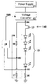
Figure 1 a illustrates a driver and control circuit according to one
embodiment of the
present invention. Power supply 11 is connected to voltage converter 12, which
provides a suitable voltage at the high end of light-emitting element load 15.
Voltage
converter 12 is internally or externally switched at high frequency in order
to change its
input voltage to a different output voltage at node 101. In one embodiment the
switching frequency may vary, for example between approximately 60 kHz to 250
kHz
or other suitable frequency range as would be readily understood. In another
embodiment the switching frequency may be fixed, for example at approximately
260 kHz, 300 kHz. Dimming of the light-emitting elements is provided by a
dimming
control signal 140, which may be a PWM, PCM or other signal, via transistor
13.
Therefore, to control the switching ON and OFF of the light-emitting elements,
the load
of the circuit is digitally switched rather than switching the voltage
converter at a low
frequency to enable or disable it as is performed in the prior art. The
present invention
has an advantage of reducing switching transients and improving response times
within
the circuit since switching the load requires the switching of only a single
transistor as
9
CA 02572335 2006-12-28
WO 2006/002519
PCT/CA2005/000969
opposed to multiple components that require switching in a voltage converter.
For
example, Figure 2a illustrates a representation of the relative current that
may flow
through the load in a circuit in which the voltage converter is switched and
Figure 2b
illustrates a representation of the relative current that may flow through the
load
according to one embodiment of the present invention in which the load is
switched.
The rise time 113 and fall time 114 of the signal illustrated in Figure 2 b
can be
significantly less than the rise time 111 and fall time 112 of the prior art
signal.
In addition, a number of factors including the junction temperature and aging
of light-
emitting elements can affect the forward current thus causing variations in
the forward
voltage drop across the light-emitting element load 15. A signal 500
representative of
this voltage drop is therefore fed back via signal conditioner 19 to voltage
converter 12,
which then adjusts its voltage output to maintain the current flowing through
the light-
emitting element load 15. Keeping the ON current through the light-emitting
elements
constant, can allow a substantially consistent and predictable brightness of
the light-
emitting elements to be obtained, and can also reduce the risk of compromising
the
lifetime of the light-emitting elements which can result from exceeding their
maximum
current rating. For example, state-of-the-art high-flux, one-watt LED packages
have a
maximum rating for average and instantaneous current of approximately 350 and
500
mA, respectively. Since the current can be controlled closely using the
present
invention, the light-emitting elements can be operated at their maximum
average current
rating without risk of exceeding their maximum instantaneous current rating.
Furthermore, multiple light-emitting element strings can be driven using a
single power
supply 21 as illustrated in Figure 3. Each light-emitting element loads 241,
242 and 243
may have its own voltage converter 221, 222 to 223 since each string may have
a
different total forward voltage. Each voltage converter 221, 222 to 223 is
thus
appropriately switched to provide the forward voltage required by the light-
emitting
element loads 241, 242 to 243, respectively to which it is connected. Feedback
signals
representative of the voltage drop across the light-emitting loads 241, 242
and 243 are
sent back to voltage converter 221, 222 and 223 via signal conditioner 291,
292 and 293,
respectively. An advantage of providing each light-emitting element string
with an
individual voltage converter is that every light-emitting element string may
be operated
approximately at its individual maximum current rating. In addition, having
different
voltage converters and a means for digitally switching the voltage for each
string can
CA 02572335 2006-12-28
WO 2006/002519
PCT/CA2005/000969
allow each light-emitting element string to be dimmed over essentially a full
range from
0% to 100%.
Voltage Conversion Means
The voltage conversion means of the present invention may be any means for
converting
a voltage of one magnitude from a power supply to a voltage of another
magnitude,
based on an input signal.
In the embodiment illustrated in Figure la, power supply 11 may be used to
convert AC
power to DC power for example, and the voltage conversion means may be a DC-to-
DC
converter. The DC-to-DC converter may be a step-down switch mode power supply
(SMPS), such as a Buck converter, for example. A Buck converter, or other
converter,
may be used with standard external components such as a diode, capacitor,
inductor and
feedback components. Buck converters are available in standard integrated
circuit (IC)
packages and together with the additional external components can perform DC-
to-DC
conversion with an efficiency of approximately 90% or higher. Examples of
other
converters that can be used in place of a Buck converter include Boost
converters, Buck-
Boost converters, Cuk converters and Fly-Back converters.
The voltage converter can operate at a high frequency to generate the
particular voltage
required by the light-emitting element string. By operating the voltage
converter at high
frequencies, high efficiency and low voltage ripple in the output voltage
signal can be
achieved. In addition, switching at high frequencies can allow the load to be
switched at
frequencies that are high enough to be outside the audible frequency range and
can also
aid in the reduction of thermal cycling of the electronic devices. This is an
advantage
over switching the voltage converter ON and OFF which is typically performed
at low
frequencies, for example typically less than lkHz.
In one embodiment in which multiple light-emitting element strings are to be
driven by a
single power supply, each light-emitting element string is connected to a
voltage
converter as illustrated in Figure 3. Each voltage converter 221, 222 to 223,
may be
individually switched at a particular frequency, to produce the voltages
desired at nodes
201, 202 to 203, respectively, in order to drive light-emitting element loads
241, 242 to
243, respectively. Thus, each light-emitting element string can be switched
from a 0 to
100% duty cycle to give essentially the maximum and minimum intensity
obtainable by
11
CA 02572335 2006-12-28
WO 2006/002519
PCT/CA2005/000969
the control signal input via transistors 231, 232 to 233. Therefore all the
light-emitting
elements can be dimmable down to very low duty cycles as well as being able to
emit
light at essentially maximum intensity. An advantage of the present invention
is that
each string can have a different forward voltage yet still have constant
current and full
dimming without large power losses.
In one embodiment in which multiple light-emitting element strings require the
same
voltage supply at the high end of the strings, these light-emitting element
strings may
have their high ends connected to a single voltage converter. The light-
emitting
elements may further be connected in a parallel and/or series configuration.
Figure if
illustrates a plurality of light-emitting elements cross connected in a series-
parallel
arrangement according to one embodiment of the present invention. This
configuration
of light-emitting elements can provide better balance the current distribution
among the
light-emitting elements, for example.
Furthermore, in one embodiment of the present invention in which multiple
light-
emitting element strings are to be driven by a single power supply, the phase
of one or
more frequency signals input to the voltage converters may be phase shifted.
Figure 4a
illustrates three signals 41, 42 and 43 that are input to three voltage
converters connected
to a power supply, wherein these signals are phase shifted relative to one
another.
Figure 4b illustrates the total current 44 drawn from the power supply during
the input
of the signals illustrated in Figure 4a. Figure 4c and Figure 4d illustrate
three input
signals 45, 46 and 47 that are not phase shifted with respect to each other
and the total
current 48 output by the power supply, respectively. Phase shifting of these
input
signals can allow the power supply load to be essentially balanced. In
addition, when
the voltage converter input signals are phase shifted, the power supply
feeding the
voltage converters may experience a higher frequency than when the input
signals are
not phase shifted. Therefore, the output from the power supply may further be
filtered
from various noise sources at lower frequencies.
Dimming Control Means
Dimming of light-emitting elements is typically done by switching the devices
ON and
OFF at a rate at which the human eye perceives the light output as an average
light level
based on the duty cycle rather than a series of light pulses. The relationship
between
12
CA 02572335 2006-12-28
WO 2006/002519
PCT/CA2005/000969
duty cycle and light intensity may therefore be linear over the entire dimming
range. As
described earlier in relation to Figure 1 a, dimming can be provided using a
dimming
control signal 140 input via transistor 13. The load can typically be switched
at a
frequency that is lower than the switching frequency of the voltage converter
12 so that
the ripple in the power supply output is averaged out over the time the load
is switched
ON. Switching the light-emitting elements at a relatively high frequency
allows them to
be switched at frequencies that are outside the audible range. In addition,
switching the
load at relatively high frequencies can reduce the effects of thermal cycling
on the
electronic devices since they are switched ON for a small fraction of time
before being
switched OFF again.
Another embodiment of the present invention is shown in Figure lb and makes
use of a
switching device 900 located between the voltage converter 12 and the light-
emitting
element load 15, which can be a FET, BJT, relay, or any other type of
switching device
which makes use of an external control input 140 to turn ON or OFF the light-
emitting
element load 15. As shown in Figure lc, this device 900 may alternately be
located on
the low side' rather than the 'high side', that is, after the light-emitting
elements rather
than before them.
In one embodiment in which there are multiple light-emitting element strings
driven by
a single power supply, each light-emitting element string may have a common
dimming
control signal, that is, the gates of transistors 231, 232 to 233 may be
connected together
and to a single dimming signal. In addition, transistors 231, 232 to 233 may
also have
individual control signals for each light-emitting element string or groups of
light-
emitting element strings.
Sensing Means
One or more sensing means can be employed to maintain the current level
through the
load. In the embodiment of Figure la, there is a voltage sensing means 104 and
a
current sensing means in the form of a resistor 16. When the light-emitting
element load
15 is switched ON, the sense voltage at node 102 generated by resistor 16 is
fed back to
converter 12 via signal conditioner 19. Resistor 16 may be replaced by another
element
for generating the sense voltage at node 102, as indicated in Figure lb, and 1
c.
Referring to the embodiments shown in Figure lb, and lc, the current sensing
device
13
CA 02572335 2006-12-28
WO 2006/002519
PCT/CA2005/000969
910 can be a fixed resistor, variable resistor, inductor, or some other
element for
generating the sense voltage signal 102 representative of the current flowing
through the
light-emitting element load 15 during the ON phase. As shown in Figure id,
current
sensing device 910 may be eliminated and in its place switching device 900 can
be used
to both switch the light-emitting elements ON and OFF, as well as provide a
means for
generating the sense voltage signal 102. However, in this scenario since the
resistance
of the switching device 900 is kept small in order to avoid excessive power
losses, this
may result in the generation of a small sense voltage signal 102 which may
reduce the
effective resolution of the system, particularly at low peak currents.
Furthermore the
variability of the resistance of a typical FET, for example, from device to
device, or at
different ambient temperatures can introduce more variability in the sense
voltage signal
than desired. In one embodiment, current sensing device 910 is a low value,
high
precision sense resistor which is stable over a wide temperature range to
ensure accurate
feedback as shown in the embodiment of Figure la.
As in Figure I a, in one embodiment the voltage sensing means 104 can comprise
a
resistor divider 17 and 18. In an alternate embodiment, the output of the
voltage
converter 101 may be connected to an input of signal conditioner 19 as shown
in Figure
1 e where the voltage signal is processed using an op amp circuit with
appropriate gain,
or other method as would be readily understood by a worker skilled in the art.
Feedback Means
The feedback means is used to maintain the desired current level flowing
through the
electronic devices being driven during the ON phase. At turn on, the current
flowing
through the electronic devices causes a signal 520 at node 102 to be generated
which is
fed back to the voltage converter 12. Voltage converter 12 then adjusts its
output
voltage to provide a constant current to the light-emitting element load 15.
When the
light-emitting element load 15 is turned OFF, the voltage sensing means 104,
is used to
maintain the feedback signal required by voltage converter 12. Therefore when
the load
is switched back ON the output voltage will still be at the same set-point as
when the
load was switched OFF, thereby substantially eliminating any current spikes or
dips in
the load. As would be readily understood by a worker skilled in the art,
signal
conditioner 19 can comprise various types of circuitry.
14
CA 02572335 2006-12-28
WO 2006/002519
PCT/CA2005/000969
An error may be introduced in the feedback signal as a result of using the
voltage
sensing means 104 in the feedback loop instead of a light-emitting element
load 15.
This error may increase as the light-emitting element ON-time decreases,
however it
may, not be significantly important at relatively low duty cycles as the
average light-
emitting element current can be much lower than its rated current, and
therefore the
accuracy of the reading is not as critical in this instance.
In one embodiment of the present invention wherein signal conditioner 19
comprises the
circuitry 191 illustrated in Figure 5, the above identified error can be small
at relatively
low duty cycles and good control of the signal from voltage converter 12 can
be
obtained. Signals 530 and 520 are the signals from nodes 103 and 102 in Figure
la,
respectively, and signal 500 is the signal fed back to voltage converter 12
from the
signal conditioning circuitry. A switch 51 controlled by a digital input
signal 510
connects signal 530 to voltage converter 12 only when the duty cycle of the
dimming
control signal 140 is below a predetermined threshold, for example 10%. Switch
51
may be a FET, BJT or any other switching means as would be readily understood.
For
higher duty cycles, a sample-and-hold circuit 52 can be used to capture signal
520
representative of the current through light-emitting elements 15 and to hold
the signal
520 in order to maintain signal 500 to voltage converter 12 even while the
light-emitting
elements 15 are in the OFF state. Resistors 53 and 54 are used to compensate
for any
gain that may be applied by sample-and-hold circuit 52. Figure 6a illustrates
one
implementation of the signal conditioning circuit 191. Switch 51 is
implemented using
a FET 511 and sample-and-hold circuit 52 is implemented by circuitry 521. As
the duty
cycle decreases, the signal on the hold capacitor 551 will have some error and
below
10%, for example, the sample-and-hold circuit 521 may have difficulty
capturing signal
520. Using external input 510, which may be another digital input from the
controller
supplying the dimming control signal, for example, switch 51 can be activated
to allow
signal 530 to override signal 520. If there is a relatively large difference
between the
predetermined voltage set point based on signal 520 and the predetermined
voltage set
point based on signal 530, then there will be a step in the output of the
voltage converter
which could cause an undesirably noticeable change in the light output from
the light-
emitting elements 15 which may result in visible flicker. Therefore, in one
embodiment
these two set points are kept at the same level.
CA 02572335 2006-12-28
WO 2006/002519
PCT/CA2005/000969
In another embodiment shown in Figure 6b, the diode shown in Figure 6a is
replaced by
a device 930 such as a FET, relay, or other form of switching device with a
control input
610. Thus the sample and hold function of 521 would be timed and controlled
externally, instead of occurring automatically as in the embodiment of Figure
6a.
In another embodiment of the present invention, the need for digital input
signal 510 is
eliminated by using the existing dimming control signal 140 to control switch
51 and
thus to determine when voltage signal 530 dominates feedback signal 500. Such
an
embodiment is illustrated in Figure 7 wherein signal conditioner 19 comprises
circuitry
192. As in circuitry 191, circuitry 192 comprises switch 51, sample-and-hold
circuit 52
and resistors 53 and 54, functioning in a similar manner. Dimming control
input signal
140 is supplied to an inverter 56, and subsequently to a filter 57 and
resistors 58 and 59.
Inverter 56 inverts the control signal 140 so that signal 530 is only allowed
to pass to
voltage converter 12 when no current is flowing through light-emitting element
load 15.
Filter 57 is used to restrict the passage of high frequency components in the
inverted
control signal. Resistors 58 and 59 are used to compensate for any gain that
may be
applied by filter 57. This embodiment can further eliminate any discrete step
changes in
the output of voltage converter 12 by operating switch 51, such as a FET, or
similar
device, in its linear region. As would be known, switches of this type are not
normally
operated in this fashion since this operation can cause significant power
loss. However
in this case, as there is only a very small current flowing through the
switch, the power
losses are negligible. Thus, at high duty cycles of dimming control signal 140
the signal
at switch 51 keeps it OFF, but as the duty cycle drops the signal controlling
switch 51
rises allowing current to flow through it. Figure 8 illustrates a schematic of
one
implementation of signal conditioning circuitry 192. Inverter 56 is
implemented by
circuitry 561 and filter 57 is implemented by low-pass filter circuitry 571.
As would be
readily understood, the functions of inverter 56 and the filtering circuitry
may be
performed using other components such as an inverter IC, or an op-amp based
active
filter. At a point determined by the characteristics of transistor 511 and
voltage sensing
means 104, the duty cycle of signal 140 can be high enough to allow current to
flow
through transistor 511, thereby allowing feedback signal 530 partially through
it. At low
enough duty cycles the switching signal will be high enough to turn transistor
511 fully
ON thus allowing feedback signal 530 to completely override feedback signal
520.
Since the resistance of transistor 511 will result in a gradual transition
between feedback
16
CA 02572335 2006-12-28
WO 2006/002519 PCT/CA2005/000969
signal 530 dominating signal 500 and feedback signal 520 dominating signal 500
there
is a smooth transition between the dominance of each signal thus eliminating
any step
changes in the output of voltage converter 12.
In another embodiment of the present invention as illustrated in Figure 9,
signal
conditioner 19 comprises circuitry 193 having a resistor 92 connected in
parallel with
resistor 17 of voltage sensing means 104 by means of a switch 91. Adding
resistor 92
and switch 91 allows the current level through voltage sensing means 104 to be
set to
various levels depending on the value of resistor 92 by means of a digital
input signal
910. When switch 91 is turned OFF the peak current level though voltage
sensing
means 104 is set to a value Io based on the resistances of the voltage
divider. When
switch 91 is then turned ON, the equivalent parallel resistance of the divider
resistor 17
and resistor 92 decreases by a fixed amount which changes signal 530 such that
the new
peak current level flowing through voltage sensing means 104 will be a
multiple of Io.
In this way activating switch 91 can produce a current boost in the feedback
circuitry
which can then be translated to the light-emitting element load 15. Used
alternately,
namely normally having switch 91 activated and then deactivating it causes the
peak
current through the voltage sensing means 104 to be reduced to some fraction
of the
initial level. This can allow the resolution of the system to be increased.
For example, if
the resolution of the dimming control signal 140 is nominally 8 bits then the
average
current through load 15 can be stepped from full current Io down to zero in
256 equal
steps. By setting the value of resistor 17 and parallel resistor 92 such that
deactivating
switch 91 causes the peak current to drop to for example 1/4 of its initial
value, then the
dimming control signal 140 duty cycle can be reduced from 100% down to 25%
thus
reducing the average current through light-emitting load 15 from Io down to
1/4 I.
Switch 91 can be subsequently deactivated and the dimming control signal 140
duty
cycle reset to 100%, and at this new peak current level the dimming control
signal
controller can now reduce the average current from 1/4 Io down to zero in 256
equal steps.
Originally there would have been 64 steps in the lowest 25%, however as
defined there
are 256 steps resulting in an increase of a factor of 4. This increase in
resolution
translates to 2 bits of resolution, and therefore the overall system
resolution has been
increased from 8 bits to 10 bits. As would be readily understood by a worker
skilled in
the art, if the resistors and switch activation were set differently then a
larger increase in
resolution could possibly be achieved. This operation can be limited in
practice by the
17
CA 02572335 2006-12-28
WO 2006/002519
PCT/CA2005/000969
accuracy of the sample-and-hold circuitry and current sense resistor 16.
Figure 10
illustrates one implementation of the signal conditioning circuitry inserted
into the
embodiment of Figure 9 wherein switch 91 is implemented by a BJT 911.
In another embodiment of the present invention, signal 910 may be replaced
with an
analog signal, generated by a DAC (digital to analog converter) in the
controller or by
external circuitry, for example, to continuously change the peak current
level, instead of
changing it between two discrete levels as previously defined. For example, by
linearly
varying the analog signal which controls switch 911 at the same rate as the
duty cycle
dimming signal 140 is changed, the combined effect would be to produce square
law
dimming of the light-emitting elements. Other variations of the control signal
are also
possible as would be readily understood.
In another embodiment as illustrated in Figure 11, a resistor divider 301
feedback path is
connected to the light-emitting element string 34 feedback loop in a wired-OR
configuration. When the dimming switch 33 is in the ON state, the current
passing
through the light-emitting elements 34 and resistor 35 is larger than the
current passing
through the resistor divider 301 namely feedback resistors 36 and 37.
Therefore, resistor
35 can dominate the feedback signal in the ON state. When switch 33 is in the
OFF
state, no current can flow through the light-emitting element string 34 or
resistor 35, and
the resistor divider circuit 301 dominates the feedback signal. In this way
the feedback
signal is maintained when the light-emitting element string 34 is turned OFF.
In another embodiment of the present invention, the resistor divider network
includes a
temperature sensitive device that changes the resistance of the resistor
divider feedback
loop as the light-emitting element junction temperature changes. For example,
the
temperature sensitive device may be a thermistor, or a standard transistor
with a known
temperature coefficient and can be used as the temperature sensitive element
in a
temperature compensation circuit as is common practice in the art. Therefore,
when the
light-emitting elements are in the OFF state, a dynamic alternate feedback
path can be
provided by the circuit. Although this embodiment may have an increased parts
count, it
may induce less error into the circuit compared to a circuit without such
temperature-
based correction.
18
CA 02572335 2013-03-11
In embodiments in which multiple light-emitting element strings are driven by
a single
power supply, components of the feedback loop of the circuit may be combined
for all
or groups of light-emitting element strings or may be separate components for
each
light-emitting element string being driven.
The embodiments of the invention being thus described, it will be obvious that
the same
may be varied in many ways. Such variations are not to be regarded as a
departure from
the invention, and all such modifications as would be obvious to
one skilled in the art are intended to be included within the scope of the
following
claims.
,
19