Note: Descriptions are shown in the official language in which they were submitted.
CA 02572785 2007-01-02
PATTERNED ELECTRICAL FOIL HEATER ELEMENT HAVING REGIONS
WITH DIFFERENT RIBBON WIDTHS
BACKGROUND OF THE INVENTION
Heaters are used in many applications where heat is required to help warm an
adjacent
area. Electrothermal heating is a common way to warm surfaces and spaces on an
aircraft by
providing heaters bonded to or integrated within the structure. It may also be
used in internal
areas of an aircraft, examples in areas such as the cockpit cabin or floors
for warming, pipes
that may contain liquids that could freeze, and even for volumetric heating of
a passenger or
air cargo compartment. In electrothermal heating systems, heat energy is
typically applied
through a metallic heating element via electrical power supplied by aircraft
or appropriate
application generators. Typical heating elements are made from foil, wire and
metallic-
coated fabrics.
Generally, the heating element of an electrothermal heater should be highly
flexible to
conform to many types of surface areas and shapes to be protected. Such
surface areas may
be either two- or three-dimensional. In addition, such heating elements should
also withstand
fatigue and foreign object damage (FOD) requirements for each particular
application.
Further, such heating elements should be capable of being specifically
designed to provide
exact power levels (heat) and uniform heat distribution to the warmed surfaces
or regions.
Most current heater elements are made from a single channel foil or wire
element
assembly 100, 200, respectively, as exemplified by the illustrations of
Figures 1 and 2,
respectively. Accordingly, a failure or break of the single element via
FOD/fatigue in most
current heater elements can reduce or eliminate the heating element's
usefulness. The prior
art also includes a movable sheet having a rectangular array of perforations
and mounted on
rollers, as disclosed in U.S. Patent No. 5,590,854; a grid-type of electrical
heating element
that is painted on, as disclosed in U.S. patent no. 6,027,075, and a mesh of
interwoven wire,
as disclosed in U.S. Patent No. 6,832,742.
SUMMARY OF THE INVENTION
In one aspect, the present invention is directed to a foil heating element.
The foil
heating element in accordance with the present invention comprises a patterned
foil sheet.
The patterned foil sheet includes a first discrete region patterned with a
first plurality of holes
1
CA 02572785 2007-01-02
forming multiple conductive ribbons and having a first sheet resistivity, and
it also includes a
second discrete region patterned with a second plurality of holes forming
multiple conductive
ribbons and having a second sheet resistivity. At least some of the multiple
conductive
ribbons in the first discrete region are in electrical continuity with at
least some of the
multiple conductive ribbons in the second discrete region, and the first
discrete region and the
second discrete region both adjoin a first junction strip of the foil heating
element.
The differences in sheet resistivity may be the result of using different hole
sizes,
different hole shapes and varying the hole center spacings in each region, or
combinations of
these, in the patterned foil sheet.
In another aspect, the present invention is directed to an electrothermal
heating
assembly comprising such a foil heating element sandwiched between first and
second layers
of material. The electrothermal heating assembly may comprises two or more
such heating
elements, and these may lie in the same plane. Also, the first and second
layers of material
may be both thermally conductive and electrically insulative.
BRIEF DESCRIPTION OF THE DRAWINGS
Figure 1 shows a first type of prior art electrothermal heating element.
Figure 2 shows a second type of prior art electrothermal heating element .
Figure 3a shows a foil heating element having a pattern of diamond-shaped
holes to
form multiple electrical paths.
Figure 3b shows a close-up of the holes seen in Fig. 3a.
Figure 4 shows a foil heating element having a pattern of keyhole-shaped holes
to
form multiple electrical paths.
Figure 5 shows a foil heating element having a pattern of circular holes to
form
multiple electrical paths.
Figure 6 shows a foil heating element having a pattern of circular holes of
varying
sizes resulting in varying-width ribbons.
Figure 7 shows a foil heating element comprising a pair of electrical buses
and depicts
the current flow between the buses.
Figure 8 shows a foil heating element comprising a pair of electrical buses in
accordance with the present invention.
Figure 9 shows an electrothermal heating assembly that incorporates a foil
heating
element of the sort seen in Fig. 8.
2
CA 02572785 2007-01-02
DETAILED DESCRIPTION OF THE INVENTION
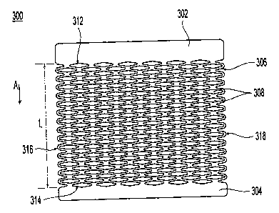
Fig. 3a shows a patterned foil sheet electrical resistance heating element 300
formed
from a single sheet of conductive material. Preferably, it is formed from a
sheet of an alloy
such as CUPRON or INCONEL , materials that are familiar to those skilled in
the art.
Other materials may also be suitable for this purpose. Such materials come in
different
thicknesses, but a sheet having an initial thickness of about 5 mil may be
preferred for this
purpose.
The foil sheet is patterned with a plurality of holes. The patterning can be
realized in
a number of ways, such as perforating, stamping, etching or by employing other
techniques to
form holes in such a foil sheet.
In one embodiment etching is employed to form the pattern of holes. Typically,
the
sheet is initially etched using a patterned mask to form a pattern of openings
and then a
surface etch of the entire surface is performed to uniformly reduce the sheet
thickness.
During this surface etch, the sheet's resistance is monitored until a desired
value is reached.
The resulting sheet is then placed in a laminate comprising electrically
insulative, but
thermally conductive layers. In one embodiment the etched sheets are
sandwiched between a
layers of KAPTON polyimide film, preferably between 1-5 mils thick. In
another
embodiment the layers may be formed of fiberglass. In still other embodiments,
epoxy or
neoprene/urethane layers may be used. Other techniques and parameters for
manufacturing
and laminating such a heating element are known to those skilled in the art.
The heating element 300 seen in Fig. 3a comprises a first junction strip 302,
a second
junction strip 304, and a patterned region 306 in-between. The first and
second junction
strips 302, 304 may serve as bus connections suitable for electrically
connecting to a power
supply and/or additional heating elements.
The patterned region 306 comprises a plurality of holes 308 separated by
ribbons 310.
As best seen in Fig. 3b, the ribbons have a ribbon width wl in areas between
the holes 308.
The patterned region 306 thus comprises multiple conductive paths, which
improve reliability
by ensuring that a single break, or even multiple breaks, in the ribbons will
not render the
heating element 300 useless.
The patterned region 306 has a length L defined by opposite first and second
ends
312, 314, respectively. A first direction, indicated by the arrow A, is
defined from the first
end 312 to the second end 314. The arrow A depicts the overall direction of
current flow in
3
CA 02572785 2010-04-26
the heating clement 300. As seen in Fig. 3, the boundaries defining the ends
312, 314 are
perpendicular to the overall direction of current flow A. The patterned region
306 is also
bounded by lateral edges 316, 318. As seen in Fig. 3a, the lateral edges 316,
318 are
scalloped, as determined by the shape of the holes 308 immediately adjacent
these edges.
In the embodiment of Fig. 3a, the first, 302 and second 304 junction strips
are on
opposite ends of the patterned region 306. The first junction strip 302 forms
a first contact
region that adjoins die first end 310 portion of patterned region 306. The
first junction strip
302, which preferably is not patterned, provides the foil sheet 300 with an
area to which a
first electrical connection may be made. The second junction strip 304 forms a
second contact
region adjacent the second and portion 312 of patterned region 306. Labe the
fast junction
strip, the second junction strip 304 also is not pattered and provides an area
to which a
second electrical connection is made.
The boles 308 in the fast patterned region 306 results is the creation of
multiple
electrical paths between the first end 312 and the second end 314.
Furthermore, the bola 308
are arranged in a direction transverse to the first direction A such that the
first patterned
region 306 is devoid of a continuous section of foil material between the
first and 312 and the
second end 314 along a line parallel to said first direction A. In other
words, when viewed
along the first direction A. there is no straight-line path of foil material
in areas away from
the lateral edges 316, 31 S. This is because the boles 308 are configured and
dimensioned
such that the multiple electrical paths in areas away from lateral edges of
said first patterned
region are all non-parallel to said first direction - the paths being forced
to travel around the
boles.
In the embodiment of Fig. 3a, the holes 308 are diamond-shaped and all holes
have
the some aim In addition, these holes 308 have rounded corners, which help
tonihniee
damage due to fatigue. The holes 308 imbue the foil sheet 300 with the above-
described
clmracteristics of multiple electrical paths, overlap, and line-of sight
properties, among
others.
As seen in Fig. 3b, the diamond-shaped holes 308 have a major axis dl that is
perpendicular to direction A and a minor axis d2 that is parallel to direction
A. In addon.,
diagonally adjacent holes 308A, 308B have a constant center spacing cl in a
first direction.
In one embodiment, the dismond-shoped holes 308 of Fig. 3a have major axis dl
of about 1.2
cm and a minor axis d2 of about 0.23 cam. Since the center spacing el of
diagonally adjacent
holes are approximately 0.48 cm, the resulting ribbon width wl is
approximately 0.10 cm. It
is understood, however, that these dmnensions may vary, depending on the
required power
4
CA 02572785 2007-01-02
and 2-D area of the foil sheet 300.
Turning to Fig. 4, the foil sheet 400 has a first junction strip 402, a second
junction
strip 404 and a patterned region 406 in-between. The patterned region 406 is
bounded by a
first end 412, a second end 414, a first lateral edge 416 and a second lateral
edge 418. The
holes 408 in the patterned region 406 are keyhole-shaped with rounded edges at
the ends of
the keyhole. A long dimension of the keyhole-shaped holes is oriented
transverse to the first
direction A representing the overall direction of current flow. The holes 408
imbue the foil
sheet 400 with the characteristics discussed above with respect to Fig. 3a
regarding the
creation of multiple electrical paths, overlap, line-of sight properties,
etc., in the direction A.
Thus, the primary difference between the embodiments of Fig. 3a and Fig. 4 is
the shape of
the holes.
In Fig. 5, the holes 508 are circular in shape and extend between the junction
strips
502, 504 formed at opposite ends 512, 514 of the patterned region 506.
In Fig. 6, the holes 608 again are circular in shape, and extend between the
junction
strips 602, 604 formed at opposite ends 612, 614 of the patterned region 606.
However, in
this embodiment, the holes 608 increase in size between the first end 612 and
the second end
614 of the pattern region 606. The holes 608A near the first end 612 are seen
to be smaller
than holes 608B near the second end 614. In particular, the holes are
monotonically
increasing in size from the first end 612 to the second end 614.
In general, it is understood that varying hole sizes, hole shapes and hole
center
spacings all influence the sheet resistivity by affecting the ribbon widths
(and thus the ribbon
cross-sectional area), the path lengths of each ribbon element, and the number
of such paths,
respectively. Such actions can change the metal volume of a given cross
section of the
heating element, thereby changing sheet resistivity.
The metal/hole patterns of the heating element embodiments described thus far
generate a robustness through their redundant circuitry. They have more
ribbons (metal
channels) than a typical current heaters seen in Figures 1 and 2,
respectively, which have a
single metal channel (foil/wire) that is interconnected in both the x and y
direction. In the
heating element embodiments described above, a breakage of several arteries by
FOD or
fatigue, for example, will result in only a minimal degradation to heating
element
functionality. Furthermore, the metal/hole foil pattern in these embodiments
may also be
tailored to specific heat densities in local areas by chemically etching the
metal ribbon
surfaces (element thickness) or edges and/or by changing the size, shape and
locations of the
holes.
5
CA 02572785 2007-01-02
Fig. 7 shows a heating element 700 formed from a single sheet of conductive
material.
The heating element 700 comprises a junction strip 702 that connects a first
bus 706A to a
second bus 706B, the buses being separated along most of their length by a
longitudinally
extending gap 730. The first bus 706A includes first and second lateral edges
716A, 718A,
respectively while the second bus 706B includes first and second lateral edges
716B, 718B.
As seen in Fig. 7, lateral edge 718A is across the gap 730 from lateral edge
716B.
In one embodiment, the junction strip is approximately 12.5 cm wide and has a
maximum height of about 1.8 cm at is center, above the gap 730. The buses
706A, 706B are
about 6.0 cm wide and the gap 730 has a width of about 0.5 cm. It is
understood that these
values are only exemplary and that other values for these parameters may be
equally suitable.
The lower portions of the buses 706A, 706B are not shown in Fig. 7. However,
the
buses 706A, 706B of the heating element 700 are connected and operated such
that current
flows through the left bus 706A towards the junction strip 702, across at
least a portion of the
junction strip in the region above the gap 730, and then flows away from the
junction strip
702 through the right bus 706B. This flow of current is depicted by the arrows
740.
The left bus 706A and the right bus 706B each comprise regions with diamond-
shaped holes of the sort seen in the embodiment of Fig. 3a. In one embodiment,
the holes are
all the same size in both buses 706A, 706B and so these buses have a uniform
pattern of
holes.
Ideally, during use, the heating element 700 has a certain output power or
heating
performance requirement. As a consequence, the heating element 700 generally
must
maintain a uniform target surface temperature within some tolerance. In the
general case, this
can be given by X Y, where X is the target surface temperature and Y is a
tolerance, both
values being given in degrees. As an example, the target surface temperature
may be 130 F
5 F. When the heating element does not meet the target temperature, cold
spots may form
in first regions 722, 724 while hot spots may form in second regions 726
between the first
regions. In the exemplary embodiment of Fig. 7, due to the specific pattern of
holes and
ribbons, the cold spots are shown to form proximate the corners of the
junction strip 702
while hot spots are shown form in regions where the bulk of the current flows
through the
junction strip 702.
Fig. 8 shows an embodiment of a heating element 800 in accordance with the
present
invention. The heating element 800 comprises a junction strip 802 that
connects a first bus
806A to a second bus 806B, the buses being separated along most of their
length by a
longitudinally extending gap 830. The first bus 806A includes first and second
lateral edges
6
CA 02572785 2007-01-02
816A, 818A, respectively, while the second bus 806B includes first and second
lateral edges
816B, 818B, respectively. As seen in Fig. 8, lateral edge 818A is across the
gap 830 from
lateral edge 816B.
Importantly, in heating element 800, the first bus 806A comprises two
patterned
regions marked 850A, 860A. In the embodiment of Fig. 8, the two patterned
regions are
separated by a boundary 870A. In terms of electrical qualities, the first
patterned region
850A has a first sheet resistance and the second patterned region 860A has a
second sheet
resistance. More particularly, the second patterned region 860A has a higher
sheet resistance
than the first patterned region 850A. Because of this increased sheet
resistance in the second
patterned region 860A, the current is forced to take another path, thus
mitigating hot spots
that otherwise might be present.
This difference in sheet resistances is the result of each patterned region
850A, 860A
having a different ribbon-to-gap ratio, which is a ratio of the area of the
ribbons that remain
to the surface area of the holes formed. In particular, the ribbon-to-gap
ratio in the first
region 850A is larger than the ribbon-to-gap ratio in the second patterned
region 860A. This
difference in ribbon-to-gap ratios can be correlated to differences in average
ribbon widths
between the holes in the two patterned regions. It should be evident to one
skilled in the art
that a smaller average ribbon width translates into a smaller ribbon cross-
sectional area, and
thus, larger sheet resistance.
By way of example, in the embodiment of Fig. 8, the ribbon-to-gap ratio in the
first
patterned region 850A is 0.62 and the ribbon-to-gap ratio in the second
patterned region
860A is 0.41. Thus, in the embodiment shown, the ribbon-to-gap ratio of the
first patterned
region 850A is a factor on the order of 1.5 times as great as the ribbon-to-
gap ratio of the
second patterned region 860A. Generally speaking, however, this factor (i.e.,
the ratio of the
larger ribbon-to-gap ratio to the smaller ribbon-to-gap ratio) can range from
1.2 to 2.5,
depending on the application. It is further understood that the ribbon-to-gap
ratios may be
tailored to the material used, the shape and size of the junction strip 802,
and the shape and
size of the bus 806A, among other factors.
In the embodiment exemplified by heating element 800, the centers of all the
holes
855A, 865A, regardless of the region 850A, 860A to which they belong, are
evenly spaced
apart. The difference in ribbon-to-gap ratios results from forming holes 855A
of one size in
the first region 850A and holes 865A of a second, larger size in the second
region 860A. It
is understood that differences in sheet resistance in each region can be
achieved by one or
more of using different hole sizes, different hole shapes and varying the hole
center spacings
7
CA 02572785 2010-04-26
in each region 850A, 860A, and combinations thereof.
In the embodiment of Fig. 8, the second region 860A comprises a wedge-shaped
area
bounded on a first side by thesecond lateral edge S 18,E on a second side by
the junction strip
802 and on a third by the boundary 870A with the first region 850A. The
boundary 870A is
S shown in this embodiment to approximately be a 45 diagonal extending from
the junction
strip 802 to the second lateral edge 81 M. As seen in this embodiment, the
boundary 870A is
staggered and follows the contours of laterally outwardly facing portions of
larger holes
865A that are on the border of the two regions 850A, 860A. It is understood
that in some
wedge-shaped embodiments, the boundary may be at an angle other than 45 , and
in still
other embodiments, the second region 860A may take on a shape other than a
wedge.
Also, in the embodiment of Fig 8, the second patterned region 860A does not
extend
all the way to the first lateral edge 816A. Instead, a predetermined width W2
of the first
patterned area 850A extends along the junction strip 802. Thus, the junction
strip 802 adjoins
a section of first patterned region 850A that extends to the first lateral
edge 816A and also
adjoins a section of second patterned area 860A that extends to the second
lateral edge 818k
Similarly, the gap 830 borders a section of second patterned region 860A that
is proximate
the junction strip 802 and also borders a section of the first patterned
region 850A that is
away from the junction strip 802.
The second bus 806B is similar in construction to the first bus 806A, having
first
lateral edge 8168 and second lateral edge 818B. Second bus 806B also comprises
first
patterned region 850B separated from second patterned region BOB by boundary
8708. In
the embodiment of Fig. 8, similar to the first bus 806A, the boundary 8708
again results in
the wedge-shape second patterned region 860B in the second bus 8068.
The heating element 800 is made by etching a foil sheet of the type described
above
using a specially designed mask having at least two different regions, each
with different hole
sizes. People skilled in the art know how to make such masks, once the pattern
is understood..
Fig. 9 shows an ell assembly 900 comprising a plurality of heating
elements 990, 992, each heating element comprising one or more junction strips
and buses.
As shown here, the heating elements 990, 992 no mounted on a thermal
conductive,
electrically insulative substrate 901. In one embodiment of an assembly, the
beating
elements 990, 992 are in the same plane and are sandwiched between two layers
of such
substrate material, as discussed above.
Heating element 990 comprises fast junction strip 902, second junction strip
904,
third junction strip 906, first bus 930 and second bus 940. A first electrical
contact 980 in
8
CA 02572785 2007-01-02
communication with the first junction strip 902 provides a first terminal for
connecting to a
power supply.
The first bus 930 comprises a first patterned region 932 which adjoins both
the first
junction strip 902 and the second junction strip 904. The first bus 930 also
comprises a
second patterned region 934 that adjoins the first junction strip 902 and a
third patterned
region 936 that adjoins the second junction strip 904. As seen in Fig. 9, the
wedge-shaped
second and third patterned regions 934, 936 are both bordered by the first
patterned region
932, the junction strips 902, 904, respectively, and by a common gap
separating bus 930 from
buses 940 and 950.
The sheet resistivities of the second and third patterned regions 934, 936
both differ
from that of the first patterned region 932. However, the sheet resistivities
of the second and
third patterned regions 934, 936 do not have to be the same - they may differ
from each
other. It is understood that the difference in sheet resistivities between one
patterned region
and another is the result of differences in hole sizes, hole shapes and/or
hole center spacings,
all as discussed above. Furthermore, this holds for all the other buses 940,
950, 960 and 970.
The second bus 940 comprises a first patterned region 942 that adjoins both
the
second junction strip 904 and the third junction strip 906, a second patterned
region 944 that
adjoins the second junction strip 904, and a third patterned region 946 that
adjoins the third
junction strip 906.
It is noted here that the second junction strip 904 provides a region where
the current
turns, as indicated by arrow 905, from first bus 930 to second bus 940. The
patterned regions
936 and 944, both of which adjoin the second junction strip 904, have higher
sheet resistivity
than the first patterned regions 932, 942, respectively, in their respective
buses 930, 940.
This helps reduce the formation of hot spots and cold spots in various
portions of the second
junction strip 904 and also in portions of the buses 930, 940 proximate the
second junction
strip 904.
The second heating element 992 includes third bus 950, fourth junction strip
908, fifth
junction strip 910, fourth bus 960, sixth junction strip 912, fifth bus 970
and seventh junction
strip 914.
The third bus 950 comprises a first patterned region 952 that adjoins both the
fourth
junction strip 908 and the fifth junction strip 910, a second patterned region
954 that adjoins
the fourth junction strip 908, and a third patterned region 956 that adjoins
the fifth junction
strip 910.
The first heating element 990 and the second heating element 992 are
electrically
9
CA 02572785 2007-01-02
connected to one another via a thermal fuse 982, which typically is a fusible
conductor
bridging third junction strip 906 and fourth junction strip 908. The patterned
regions 946 and
954 on either side of the thermal fuse 982 help ensure more uniform current
flow in the
adjacent junction strips 906, 908 belonging to buses 940, 950, respectively.
The fourth bus 960 comprises a first patterned region 962 that adjoins both
the fifth
junction strip 910 and the sixth junction strip 912, a second patterned region
964 that adjoins
the fifth junction strip 910, and a third patterned region 966 that adjoins
the sixth junction
strip 912.
The fifth junction strip 910 provides a region where the current turns, as
indicated by
arrow 911, from third bus 950 to fourth bus 960. The patterned regions 956 and
964, both of
which adjoin the fifth junction strip 910, have higher sheet resistivity than
the first patterned
regions 952, 962, respectively, in their respective buses 950, 960. This helps
reduce the
formation of hot spots and cold spots in various portions of the fifth
junction strip 910 and
also in portions of the buses 950, 960 that are close to the fifth junction
strip 910.
The fifth bus 970 comprises a first patterned region 972 that adjoins both the
sixth
junction strip 912 and the seventh junction strip 914, a second patterned
region 974 that
adjoins the sixth junction strip 912, and a third patterned region 976 that
adjoins the seventh
junction strip 914.
The sixth junction strip 912 provides a region where the current turns, as
indicated by
arrow 913, from fourth bus 960 to fifth bus 970. The patterned regions 966 and
974, both of
which adjoin the sixth junction strip 912, have higher sheet resistivity than
the first patterned
regions 962, 972, respectively, in their respective buses 960, 970. This helps
reduce the
formation of hot spots and cold spots in various portions of the sixth
junction strip 912 and
also in portions of the buses 960, 970 that are close to the sixth junction
strip 912.
The seventh junction strip 914 provides a region where the current turns, as
indicated
by arrow 915, from fifth bus 970 as it travels down an elongated portion of
the seventh bus
towards second electrical contact 984. The third patterned region 976 of the
fifth bus 970
which adjoins the seventh junction strip 914, has a higher sheet resistivity
than the first
patterned region 972 of the fifth bus. This helps reduce the formation of hot
spots and cold
spots in portions of the seventh junction strip 912 and also in portions of
the fifth bus 970 that
are close to the seventh junction strip 914.
The second electrical connector 984 is in communication with the seventh
junction
strip 914 and provides a second terminal for connecting to a power supply. The
seventh
junction strip 914 is provided with the elongated portion so that the second
electrical contacts
CA 02572785 2010-04-26
984 is in close physical proximity to the first electrical contact 980. This,
the first and
second electrical contacts 980, 984 are sufficiently close to one another that
they are
connectable to corresponding contacts of a power cable having two or more
wires.
As seen in the assembly of Fig. 9, in a patterned foil hung element, changes
in sheet
resistivity though varying hole attributes in regions where the current turns,
may be used to
reduce the likelihood of hot spots and cold spots. This may facilitate
attaining temperature
uniformity specification of such foil heating elements, and assemblies
incorporating the
same.
People skilled in the an know how to make and use electric heaters for
aircraft de-
icing and other applications, as exemplified by U.S. Patent Nos. 5,475,204,
5,590,854,
6,027,075, 6,237,874 and 6,832,742.
The above description of various embodiments of the invention is intended to
describe
and illustrate various aspects of the invention, and is not intended to limit
the invention
thereto. Persons of ordinary skill in the art will understand that certain
modifications may be
made to the described embodiments without departing from the invention, All
such
modifications are intended to be within the scope of the appended claims.
it