Note: Descriptions are shown in the official language in which they were submitted.
CA 02573085 2007-01-05
WO 2006/016970 PCT/US2005/021531
HIGH SPEED INTEGRATED CIRCUIT
FIELD OF THE INVENTION
[0001] The present invention relates generally to digital communication
interface designs and high speed circuit designs.
BACKGROUND OF THE INVENTION
[0002] A signal line is a conductor used to transmit electrical signals
between
various devices in an electronic system or between devices located in two
separate
electronic systems. Output driver circuits contained on each device are used
to buffer
signals originating from the device so that they may be driven onto the signal
lines.
[0003] There are well known single-ended output driver circuits (e.g., TTL
drivers) that are simple to use. However, most of these previously disclosed
driver
circuits are not suitable for high speed signals due to their low maximum
operating
frequency and high noise. For example, the maximum operating frequency of a
single-ended CMOS driver circuit IDT74FCT3807D/E, which is available from
Integrated Device Technology, Inc. of Santa Clara, California, is 166 Mhz. As
another example, the maximum operating frequency of a single-ended 1 input to
5
outputs CMOS driver circuit PI49FCT3802, which is available from Pericom
Semiconductor Corporation of San Jose, California, is 156 Mhz. Other
manufacturers such as On Semiconductors, Philips Semiconductors, Integrated
Circuit Systems, Inc., also offer similar products that have similar maximum
operating frequencies.
[0004] For driving high speed signals, differential drivers are often used. A
typical differential driver 10 is schematically illustrated in FIG. 1. The
differential
driver 10 includes data inputs 12a-12b for inputting a differential data
signal, and
data outputs 14a-14b for providing the differential signal to a differential
receiver 16
via signal lines. The arrangement of FIG. 1 is well known to have high
operating
frequency. However, differential interface designs have disadvantages as well.
First,
-1-
CA 02573085 2007-01-05
WO 2006/016970 PCT/US2005/021531
every differential signal requires two or more signal lines. Therefore, a
differential
I/O interface will require at least twice the number of pins than a single-
ended I/O
interface, resulting in, a larger chip. Furthermore, high speed systeins
generally
require careful matching of the electrical length of the signal lines such
that
synchronous signals may be received witll a common clock and a common phase.
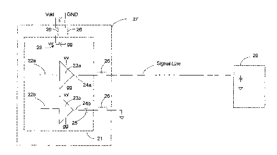
This design requirement is sometimes known as "length matching" or "delay
matching." A wide differential interface will require a large number of signal
lines,
necessarily complicating the length matching effort and increasing the cost of
manufacture. In some instances, length matching many signal lines may be
impossible on tightly packed circuit boards. Thus, at least in some electronic
systems, it is not desirable to use differential interfaces.
[0005] Accordingly, a single-ended output interface design that
communicates single-ended signals at a performance level that is comparable to
that
of a differential interface may be desirable.
SUMMARY OF THE INVENTION
[0006] An embodiment of the invention is a single-ended output interface that
uses a differential driver as a design backbone. Unlike a coanventional
differential
interface, which typically has two or more outputs for providing an output
signal and
its complement, the differential driver of the present embodiment has one of
its
outputs coupled to drive a signal onto a signal line, while a complementary
output is
not used for signal transmission. Rather, the complementary output is
considered
logically redundant and is terminated, for example, by coupling to package
ground or
system ground via a capacitor. A result of terminating a logically redundant
output is
that the performance of the output interface may be significantly improved
over
conventional designs.
[0007] In one embodiment of the invention, multiple differential drivers are
implemented within an integrated circuit that has a package ground plane.
According
to this embodiment, each "unused" output of the differential drivers may be
terminated at the package ground plane through a capacitor. The package ground
plane itself may be coupled to one or more GND pins. In this way, very few
pins are
needed by the "unused" outputs. Furthermore, only one signal line is needed
for each
-2-
CA 02573085 2007-01-05
WO 2006/016970 PCT/US2005/021531
single-ended output signal. In comparison to conventional differential
interfaces,
where two pins and two signal lines are required for each differential signal,
the
number of pins and signal lines used by the present embodiment may be
significantly
smaller.
[0008] Another embodiment of the invention is an integrated circuit having a
single-ended input and multiple single-ended outputs, for instance a clock
driver.
Within the integrated circuit, the input signal is first converted into a
differential
signal. The differential signal is distributed to the multiple differential
drivers. Each
differential driver may have an output for providing a single-ended output
signal and
an "unused" output, which terminates one component of the differential signal.
Each
"unused" output may be coupled to package ground or system ground via a
capacitor
for the purpose of iunproving the perforinance of the other output.
[0009] Another embodiment of the invention is an integrated circuit having
single-ended inputs and single-ended outputs. The single-ended outputs are
implemented using differential drivers each having one output that is
"unused."
Within the integrated circuit, differential signals may be originated,
processed and
distributed to the multiple differential output driver circuits. Each
differential driver
may have an output for providing a single-ended output signal and an "unused"
output. The "unused" output of each differential driver may be coupled to
package
ground or system ground via a capacitor for the purpose of improving the
perforinance of the other output. Circuits that process differential signals
within the
integrated circuits may be implemented with differential standard cells in
accordance
with some embodiments of the invention.
[0010] Yet another embodiment of the invention is an integrated circuit
having a logic core and a plurality of output pads or I/O pads coupled to the
logic
core. The output pads or I/O pads may include circuits for receiving single-
ended
signals from the logic core, converting the single-ended signals into
differential
signals, and providing one component of each differential signal as a single-
ended
output signal. Another component of each differential signal is terminated,
for
example, by coupling to package ground or system ground via a capacitor.
[0011] Yet a further aspect of the invention provides a method of designing a
high speed circuit. According to this aspect of the invention, a logic-level
schematic
-3-
CA 02573085 2007-01-05
WO 2006/016970 PCT/US2005/021531
for a first circuit is converted to a transistor level schematic. A
complementary
circuit is designed and added to the transistor level schematic. The
complementary
circuit, in one embodiment, performs a logic function that is complementary to
the
logic function of the first circuit and has a same number of nodes as the
first circuit.
Furthermore, the nodes in the complementary circuit are complementary to the
corresponding nodes in the first circuit. In addition, the rise/fall time of
each node in
the first circuit matches the fall/rise time of a corresponding node in the
complementary circuit. The trace length between certain nodes of the
complementary
circuit may have to match the trace length between corresponding nodes of the
first
circuit. The pull-up and pull-down currents at the appropriate nodes of the
first
circuit may have to match the currents at the corresponding nodes at the
complementary circuit. The resulting circuit design is called a "differential
circuit,"
which is capable of operating at a clock speed significantly higher than the
clock
speed at which the first circuit is capable of operating. The resulting
transistor level
schematic, which may include twice the transistors than the original
transistor level
schematic, is then converted to a logic-level schematic for the differential
circuit.
According to one embodiment of the invention, the logic-level schematic for
the
differential circuit is sometimes called a "voltage mode" differential cell."
[0012] According to one embodiment, the "voltage mode" differential cell
design methodology according to this aspect of the invention is applicable to
the
design of digital logic circuits (e.g., CMOS circuits), analog circuits,
and/or mixed
signal circuits.
BRIEF DESCRIPTION OF THE DRAWINGS
[0013] The invention will now be described with reference to the
accompanying drawings which illustrate various example embodiments of the
invention. Throughout the description, similar reference names may be used to
identify similar elements.
[0014] FIG. 1 depicts a differential driver.
[0015] FIG. 2 depicts an output driver circuit that uses a differential driver
as
a backbone according to an embodiment of the invention.
[0016] FIGS. 3A-3F depict examples of various embodiments of the
-4-
CA 02573085 2007-01-05
WO 2006/016970 PCT/US2005/021531
invention.
[0017] FIGS. 4A-4D depict an example implementation of a circuit in
accordance with an embodiment of the invention.
[0018] FIG. 5 depicts simulation results of the output interface design of
FIGS. 4A-4B.
[0019] FIG. 6 depicts a schematic of a known clock driver circuit.
[0020] FIG. 7 depicts a schematic of a clock driver circuit according to an
einbodiment of the invention.
[0021] FIG. 8 depicts an integrated circuit package where unused outputs of
the differential drivers are coupled to the common ground plane, in accordance
with
an embodiment of the invention.
[0022] FIGS. 9A-9D depict integrated circuits according to embodiments of
the invention.
[0023] FIG. 10 depicts a ring oscillator circuit implemented according to an
embodiment of the invention.
[0024] FIG. 11A depicts a crystal oscillator circuit implemented according to
an embodiment of the invention.
[0025] FIG. 11B depicts a crystal oscillator circuit implemented according to
another embodiment of the invention.
[0026] FIGS. 12A-12G depict example differential standard cells according
to embodiments of the invention.
[0027] FIG. 13A depicts a voltage-mode differential comparator that may be
used in another example impleinentation of an output driver circuit in
accordance
with an embodiment of the invention.
[0028] FIG. 13B depicts a comparator circuit that is known in the art.
[0029] FIG. 14 depicts a high speed serial bus system that may be
implemented according to an embodiment of the invention.
[0030] FIG. 15 depicts a high speed wireless communication system that may
be implemented according to an embodiment of the invention.
-5-
CA 02573085 2007-01-05
WO 2006/016970 PCT/US2005/021531
[0031] FIG. 16A depicts an example half-adder circuit implemented
according to an embodiment of the invention.
[0032] FIG. 16B depicts a half-adder circuit that is known in the art.
[0033] FIG. 17A depicts an example 4-to-1 multiplexer circuit implemented
according to an embodiment of the invention.
[0034] FIG. 17B depicts a 4-to-1 multiplexer circuit that is known in the art.
[0035] FIG. 18 is a diagram depicting an example transistor-level
implementation a differential NOR gate of FIG. 12B.
[0036] FIG. 19 is a diagram depicting an example transistor-level
implementation a differential NAND gate of FIG. 12A.
[0037] FIG. 20 is a flow diagram depicting an example IC design process
according to one aspect of the present invention.
[0038] FIG. 21 depicts a transistor-level schematic diagram of an exemplary
3-input voltage-mode differential NAND cell according to an embodiment of the
invention.
[0039] FIG. 22 depicts a transistor-level schematic diagram of an exemplary
3-input voltage-mode differential NOR cell according to an embodiment of the
invention.
[0040] FIG. 23 depicts a transistor-level schematic diagram of an exemplary
2-input voltage-mode differential XOR cell according to an embodiment of the
invention.
[0041] FIG. 24 depicts a transistor-level schematic diagram of an exemplary
2-input voltage-mode differential XNOR cell according to an embodiment of the
invention.
[0042] FIG. 25 depicts a flow diagram for a high speed circuit design
methodology according to one embodiment of this aspect of the invention.
[0043] FIG. 26A depicts an example divide-by-three counter circuit
implemented according to an embodiment of the invention.
[0044] FIG. 26B depicts a truth table for the divde-by-three counter circuit
of
FIG. 26A.
-6-
CA 02573085 2007-01-05
WO 2006/016970 PCT/US2005/021531
[0045] FIG. 26C depicts input equations for the divde-by-three counter
circuit of FIG. 26A.
[0046] FIG. 27 depicts a divide-by-three counter circuit that is known in the
art.
[0047] FIG. 28 depicts a flow diagram for a high speed circuit design
methodology according to another aspect of the invention.
[0048] FIG. 29 depicts an integrated circuit according to another embodiment
of the invention.
[0049] FIG. 30 depicts an integrated circuit according to yet another
embodiment of the invention.
DETAILED DESCRIPTION OF PREFERRED EMBODIMENTS
[0050] Various features of the invention, including specific implementations
thereof, will now be described. Throughout the description, the term
"differential
signal" refers to a signal that is carried by more than one signal lines, and
thus a
differential signal includes two or more component signals that may be
complementary to each other. If the sum of two time-varying signals always
approximately equals a constant value, such as zero, the signals are said to
be
"complementary" to each other. The term "single-ended signal" refers to a
signal that
is carried by a single signal line. Furthermore, the terms "driver" and
"driver circuit"
are used synonymously.
[0051] Throughout the description, the terin "unused output" refers to an
output of a differential output driver that is not used to provide a signal to
a receiver,
or one that is not used to drive a signal line. The term "unused output" may
also refer
to an output of a differential output driver that may be coupled to package
ground,
system ground, voltage source, etc., via a capacitor. Additionally, the term
"unused
output" may refer to an output of a differential output driver that drives a
component
of a differential signal to package ground, system ground, voltage source,
etc., via a
capacitor. An "unused signal" herein may refer to a signal that is provided by
an
unused output and that is not provided to a signal receiver. A more specific
meaning
for the above terms may be inferred by context.
-7-
CA 02573085 2007-01-05
WO 2006/016970 PCT/US2005/021531
[0052] Furthermore, the terms "couple" and "coupled" may describe a direct
or an indirect connection. For example, a node may be connected to one end of
a
capacitor, and another end of the capacitor may be connected to system ground.
The
node is said to be "coupled" to system ground even though the connection is an
indirect one.
[0053] The various features of the invention set forth herein may be embodied
within a wide range of integrated circuits including, but not limited to,
signal drivers,
clock drivers, oscillators (e.g., ring oscillators, crystal oscillators),
serial bus drivers,
ethernet drivers, optical transmitters, memory controllers, memories,
microprocessors, wireless transmitters, and power amplifiers, some of which
may be
found in computer systems and wireless devices (e.g., laptop computers,
wireless
telephones and personal digital assistants). Also, it should be understood
that some
implementations described herein may be specific to CMOS technology and that
features of the invention may be applicable to other integrated circuit
technologies as
well.
[0054] Referring to FIG. 2, there is schematically illustrated an output
driver
circuit in accordance with an embodiment of the invention. The output driver
circuit
includes inputs 22a-22b for receiving a differential signal, and drivers 23a-
23b for
providing the differential signal through outputs 24a-24b. According to an
embodiment of the invention, the differential signal includes two
complementary
signal components. Note that driver 23a drives one of the complementary
signals as
a single-ended output signal to receiver 29 via a signal line. The other one
of the
complementary signals is unused and is terminated, for instance by coupling
the
output 24b to system ground (GND) via a capacitor 25. As a result of
terminating the
unused signal, which is considered logically redundant to and inverse of the
"used"
signal, the performance'of the output driver circuit may be significantly
better than
those of conventional single-ended driver designs.
[0055] In a preferred embodiment, the driver 23a and driver 23b are
connected to the same voltage source and the same ground. In one embodiment of
the invention, the circuit in FIG. 2 may be implemented using TTL-CMOS, which
may minimize static current requirement and provide high power output. For
example, a TTL-CMOS circuit according to the invention may have a static
current
that is close to zero (e.g., 0.1 A) and may have a power output of 3 V or
more. A
-8-
CA 02573085 2007-01-05
WO 2006/016970 PCT/US2005/021531
power output of 3 V or more is significantly higher than the power output of
an
LVDS (Low Voltage Differential Signaling) differential driver, which is
typically
about 350 mV. Thus, the invention may allow one to achieve high frequency
without
compromising performance for low static current and high output power.
[0056] Also depicted in FIG. 2 are die 21, package 27, and inductors 26
representative of the inductance associated with the bonding wires of the
package 27.
Also shown in FIG. 2 is a decoupling capacitor 28. The decoupling capacitor 28
may
be located on the die 21, outside the die 21 but inside the package 27, or
outside the
package 27.
[0057] According to one embodiment of the invention, the unused output of
the driver 23b may be terminated inside or outside the package, and the
capacitor 25
may be placed inside the die 21, outside the die 21 but within the package 27,
or
outside the package 27. Furtherinore, the capacitor 25 may be coupled to a
voltage
source, such as Vcc, or any pre-determined voltage.
[0058] FIGS. 3A-3F depict several ways of terminating the unused output.
In light of the disclosure herein, one of ordinary skill in the art would
appreciate that
many other ways of terminating unused outputs are within the scope of the
principles
of the invention disclosed herein. For instance, in embodiments where a
capacitor is
illustrated, one of ordinary skill in the art would appreciate that an
inductor and/or
resistor may be used in combination with or in lieu of the capacitor,
depending on the
application and loading. Many other combinations and permutations of
resistance,
capacitance and inductance values and their locations are possible.
[0059] FIG. 3A schematically depicts an output driver circuit according to an
embodiment of the invention. The output driver circuit includes a differential
driver
30 that is configured to receive a differential signal. Unlike outputs of
conventional
differential drivers, one output of the differential driver 30 provides a
single-ended
output signal to a signal line, and another output 32 is unused and is
terminated. As
shown in FIG. 3A, a capacitor 34 couples the unused output 32 to GND. In one
embodiment, the capacitor 34 may have the same capacitance as the load, which
is
represented by capacitor 38 and which is typically a signal I/O receiver. In
one
implementation, the capacitance of capacitor 34 may be approximately half-way
between the maximum loading capacitance and minimum loading capacitance of the
-9-
CA 02573085 2007-01-05
WO 2006/016970 PCT/US2005/021531
integrated circuit, and the capacitance may vary depending on application. In
another
implementation where the output load capacitor 38 has a maximum value of about
15
pf, the capacitance of the capacitor 34 is preferably between approximately 5
pf to
approximately 13 pf. In the embodiment shown in FIG. 3A, the capacitor 34 is
implemented outside the die 35 and the chip package 31, for instance on a
printed
circuit board (PCB). Also shown in FIG. 3A are inductors 36a-36b, which
represent
the inductance within the package 31.
[0060] FIG. 3B schematically depicts a differential driver 30 whose unused
output 32 is temiinated outside the package 31 via a capacitor 34a and an
inductor
36b. Note that in this embodiment the capacitor 34a is located on the saine
die 35 as
the differential driver 30. As in the embodiment shown in FIG. 3A, the
capacitor 34a
may have the same capacitance as the load. In one implementation, its
capacitance
may be approximately 5 - 13 pf. Note that this capacitance may vary depending
on
the application.
[0061] FIG. 3C schematically depicts a differential driver 30 whose unused
output 32 is terminated inside the package 31, in accordance with an
embodiment of
the invention. In this embodiment, the unused output 32 is terminated at a
ground
plane of the package 31. The ground plane is in turn coupled to an external
ground
(e.g., system ground) via a connector or pin 39.
[0062] FIG. 3D schematically depicts another embodiment of the invention.
In this embodiment, the unused output 32 of the differential driver 30 is
coupled to an
external voltage source Vcc via a capacitor 34. Note that in this embodiment,
the
load is coupled to Vcc as well.
[0063] FIG. 3E schematically depicts yet another embodiment of the
invention. In this embodiment, the unused output 32 of the differential driver
30 is
terminated at a pre-determined voltage via a capacitor 34. Note that in this
embodiment, the load is coupled to the same pre-determined voltage as well.
[0064] FIG. 3F schematically depicts yet another embodiment of the
invention. In this embodiment, capacitor 34a and resistor 37 are located on
die 35.
Preferably the resistor 37 may have approximately the same resistance as the
series
resistor R on the signal line. The series resistor R may be implemented to
suppress
the reflection signal on the signal line.
-10-
CA 02573085 2007-01-05
WO 2006/016970 PCT/US2005/021531
[0065] It should be noted that the output driver circuits and the receivers
may
not necessarily be implemented within the same system. In other words, the
signal
lines connecting the output driver circuits and the receivers are not limited
to signal
traces of a printed circuit board (PCB). The output driver circuits according
to the
present invention may be used to drive signals across cables (e.g., CAT-6
cables) or
other types of electrical connections. According to one embodiment, the output
driver circuit may drive signals that have a large voltage swing. Thus, the
signals
may be carried for a large distance. Furthermore, in some embodiments, the
signal
lines may not be strictly electrical connections. Rather, a signal line may be
any
signal path, which may include electrical connections, optical connections,
wireless
connections, and/or any other type of conduits, and/or any combination
thereof.
[0066] Referring now to FIGS. 4A-4D, there is shown schematically an
example implementation of a circuit according to an embodiment of the
invention. In
FIGS. 4A-4D and other drawings, "gg" indicates chip ground, and "vv" indicates
chip voltage Vdd. This illustrated implementation may be sub-divided generally
into
three stages. The first stage 410, which includes inverter 412 and
transmission gate
414, converts the input signal into a differential signal. Naturally, the
inverter 412
causes a small signal propagation delay. A function of the transmission gate
414 is to
provide sufficient delay such that the resulting differential signal has
complementary
components. In an alternate embodiment, the transmission gate 414 may be
replaced
by an appropriate RC circuit. In that embodiment, the RC circuit may have RC
characteristics that generally match those of the inverter 412.
[0067] With reference still to FIG. 4A, the first stage 410 may be coupled to
an electrostatic discharge (ESD) circuit 416 that protects the input circuit
from
electrostatic discharge. Also note that in this variation the ESD circuit 416
utilizes
the transmission gate 414 to provide the ESD protection function. The ESD
circuit
416 further provides a 5V I/O tolerant function when the overall circuit is
driven by 3
V to 3.6 V. Furthermore, the first stage 410 may include a differential
comparator
circuit, an example of which is shown in FIG. 13A (described further below),
for
receiving differential signals.
[0068] The second stage 420 includes two inverter circuits 422a-422b
coupled to inverter 412 and transmission gate 414, respectively, to receive
the
differential signal. Note that the second stage 420 is optional. In another
-11-
CA 02573085 2007-01-05
WO 2006/016970 PCT/US2005/021531
embodiment of the invention, outputs of the first stage 410 may connect
directly to
inputs of the third stage 430. In other embodiments, the second stage 420 may
include any differential logic circuit. For instance, the second stage 420 may
include
differential latches, differential flip-flops, etc., in place of the inverter
circuits 422a-
422b.
[0069] According to an embodiment of the invention, the second stage 420
may include circuits capable of processing differential or coinplementary
signals.
These circuits may be implemented with a plurality of differential standard
cells that
have differential inputs and differential outputs. Examples of some
differential
standard cells of the invention are illustrated in FIGS. 12A-12G, which are
described
further below.
[0070] It should be appreciated by one skilled in the art having the benefit
of
the present disclosure that the differential standard cells of the invention
are different
from previously disclosed differential circuits such as differential current
mode logic.
For instance, current mode logic circuits have static currents (and current
sources),
and thus they are not suitable for VLSI implementation. In contrast, circuits
built
according to the differential standard cells of the invention may not have
static
currents (except for leakage current), and thus they are suitable for VLSI
implementation. It should also be appreciated by one skilled in the art having
the
benefit of the present disclosure that the differential standard cells shown
in FIGS.
12A-12G and FIG. 13A (described below) do not represent an exhaustive list,
and
that many other differential standard cell designs consistent with the
principles of the
invention are possible and are within the scope of the invention. Since the
differential standard cells are not using current source, the term "voltage
mode" is
used herein to describe the differential standard cells and to distinguish
them from
current mode logic.
[0071] The third stage 430, which is shown in FIG. 4B, may include multiple
inverter circuits although only two inverter circuits 432a-432b are
illustrated. In this
embodiment, the inverter circuits 432a-432b are coupled to the inverter
circuits 422a-
422b (FIG. 4A), respectively. In other embodiments, the connections may be
swapped. That is, the inverter circuit 432a may be coupled to inverter circuit
422b,
and inverter circuit 432b may be coupled to inverter circuit 422a.
-12-
CA 02573085 2007-01-05
WO 2006/016970 PCT/US2005/021531
[0072] The third stage 430 further includes transistor 442, which acts as a
capacitor, and ESD Diodes 444. According to an embodiment of the invention,
the
inverter circuit 432a provides the "unused output" of the differential driver
of FIGS.
4A-4B. According to one embodiment of the invention, the output 446 is coupled
to
ground plane of an integrated circuit package such that the output 446 may be
coupled to GND when the integrated circuit is in operation. The output 448 may
be
coupled to an output pin of the integrated circuit such that the output 448
may drive a
signal line when the integrated circuit is in operation.
[0073] FIG. 4C depicts a decoupling capacitor 440, and FIG. 4D depicts an
ESD protection circuit 450. Both the decoupling capacitor 440 and the ESD
protection circuit 450 may be part of the same integrated circuit as the
output driver
circuits. The decoupling capacitor 440 is for providing a clean voltage source
and
ground within the die, and the ESD protection circuit 450 is for protecting
the circuits
from electrostatic damage. Other circuitry may be implemented as part of the
integrated circuit as well. The capacitance of the decoupling capacitor 440
can be
very small or very large and may vary from one implementation to another as
long as
it is capable of providing a clean voltage source and ground within the die.
[0074] According to an embodiment of the invention, the circuits of FIGS.
4A-4D are implemented using CMOS technology. PMOS transistors shown in
FIGS. 4A-4B have the following device parameters: m = 4, w = 80 m, L = 0.35
m
(except PMOS transistors 442). NMOS transistors shown in FIGS. 4A-4B have the
following device parameters: in = 4, w = 40 m, L = 0.35 m. PMOS transistor
442
has the following device parameters: m= 3, w= 46.5 m, L = 12.9 m. The NMOS
transistor 440 (FIG. 4C) has the following device parameters: m = 3000, w = 30
m,
L=20 m. The NMOS transistor 450 (FIG. 4D) has the following device
paraineters:
in = 8, w = 40 m, L = 0.35 m. These implementation details are provided for
completeness purposes only and such details should not be construed to limit
the
scope of the invention. Embodiments of the present invention may be
iinplemented
in many other ways using different technologies, different types of
transistors and
different device parameters.
[0075] Referring now to FIG. 13A, there is shown a "voltage mode"
differential comparator 130 that may be used as an alternative to circuits 412
and 414
-13-
CA 02573085 2007-01-05
WO 2006/016970 PCT/US2005/021531
of FIG. 4A. The circuits 412 and 414 are configured to receive a single-ended
input
signal and to convert the single-ended input signal into a differential
signal. Unlike
circuits 412 and 414, the differential comparator 130, which includes
comparator
circuits 130a-130b, is configured to receive a differential signal and provide
the
comparison result and its complement (or inverse) to other circuits, for
instance
circuits 422a and 422b. According to an embodiment of the invention, the
differential comparator circuit 130 may be used for receiving differential
signals
originated from another portion of the integrated circuit or outside of the
integrated
circuit. The differential comparator circuit 130 may be used also for
receiving
LVDS, LVPECL, HSTL and other differential signals that have a small voltage
swing. In some embodiments where the differential signals have large voltage
swings, the differential signals may be fed directly to circuits of the second
stage 420
or the third stage 430.
[0076] Attention now turns to FIG. 5, which depicts simulation results of the
output driver circuit design of FIGS. 4A-4D. The simulation results are
obtained by
using TSMC 0.35 m BSIM-3 spice model. The output frequency of approximately
1 Ghz is achievable with a 5 pf load. In an actual implementation, the output
frequency of approximately 1 Ghz is achievable with a load of approximately 2
pf
from a single-ended 1 input to 5 outputs CMOS driver circuit. For the purposes
of
illustration, the maximum operating frequency of a pin-to-pin compatible
single-
ended 1 input to 5 outputs CMOS driver circuit PI49FCT3802, which is available
from Pericom Semiconductor Corporation of San Jose, California, is 156 Mhz.
[0077] Referring now to FIG. 6, there is shown a schematic of a known
CMOS clock driver integrated circuit 60, an example of which is an integrated
circuit
bearing model number IDT74FCT3807D/E, which is available from Integrated
Device Technology, Inc. of Santa Clara, California. As shown, this clock
driver
circuit has an input for receiving a clock signal, and ten outputs for
distributing the
clock signal to ten devices. According to a published specification from the,
manufacturer, the maximum operating frequency of the aforementioned clock
driver
circuit is 166 Mhz. In many applications, an operating frequency higher than
166
Mhz is often desired.
[0075] FIG. 7 depicts a schematic of a clock driver integrated circuit 70
according to an embodiment of the invention. As shown the clock driver circuit
-14-
CA 02573085 2007-01-05
WO 2006/016970 PCT/US2005/021531
includes an input inverter 72 and a transmission gate 73 for receiving an
input signal,
and output drivers 74a-74j for providing multiple output signals. Note that,
although
the input signal and the output signals are single-ended signals, differential
signals
are communicated within the integrated circuit to the output drivers 74a-74j.
As
shown in FIG. 7, the input inverter 72 and the transmission gate 73 convert
the input
signal into a differential signal and provide the differential signal to the
output drivers
74a-74j. Furthermore, output drivers 74a-74j each have an unused output such
that
one component of each output differential signal is not transmitted. According
to the
present embodiment, the clock driver integrated circuit may achieve an
operating
frequency of 1 Ghz by using a 0.35 m CMOS process technology. This
performance
level is significantly higher than the maximum performance level of the
conventional
CMOS clock driver shown in FIG. 6. In light of the disclosure herein, one of
ordinary skill in the art would appreciate that the circuit shown in FIG. 7
may be
implemented with other semiconductor technologies, such as 0.25, 0.18, 0.09 m
processes and/or GaAs, BiCMOS, and BJT processes, which may further enhance
the
frequency performance of the circuit.
[0079] In one embodiment of the invention, multiple differential drivers are
implemented within in an integrated circuit. In this embodiment, the unused
output
of each differential driver may be coupled to an external ground (e.g., system
ground)
via individual GND pins. However, in some applications having an individual
GND
pin for each output driver circuit may be undesirable because the increased
number of
pins may increase the size and cost of the integrated circuit.
[0080] In another embodiment of the invention, multiple unused outputs may
be coupled together to a package ground plane of the integrated circuit. The
package
ground plane is coupled to one or more GND pins, which are designated to be
coupled to an external ground (e.g., system ground). In other words, one or
more
GND pins may be shared by all the unused outputs of the output driver
circuits. In
this way, a single GND pin may support a wide output interface.
[0081] An integrated circuit package 84 where unused outputs of the output
driver circuits are coupled to a package ground plane is depicted in FIG. 8.
As
illustrated, multiple bond wires connect the bond pads that correspond to the
unused
outputs of the output driver circuits to the Ground Plane 80, which is itself
connected
to GND Pins 82a-82e via other bond wires. Note that GND Pins 82a-82e are not
- 15 -
CA 02573085 2007-01-05
WO 2006/016970 PCT/US2005/021531
designated for signal transmission purposes but are designated to be coupled
to
ground.
[0082] In another embodiment of the invention, unused outputs of the output
driver circuits may be coupled together to a common node within the die or
within
the chip package. The common node may be coupled to ground node, a voltage
source, or a node with a pre-determined voltage so as to terminate the unused
signals.
[0083] Attention now turns to FIG. 9A, which depicts schematically an
integrated circuit 90a according to an embodiment of the invention. The
integrated
circuit 90a includes core logic 94a, which may include, for instance, CMOS
logic
circuits such as a central processing unit (CPU) core, and/or a memory core
(e.g., a
DRAM core). The integrated circuit 90a further includes output drivers (or
"output
pads") 20a for providing output signals.
[0084] According to the embodiment shown in FIG. 9A, an output driver 20a
receives a single-ended signal from the core logic 94a via input 22a. The
output
driver 20a, which may include circuits shown in FIGS. 4A-4B, converts the
single-
ended signal into a differential signal, provides one of the component of the
differential signal as an output signal via output 24a, and terminates the
other
component signal via output 24b and capacitor 34a.
[0085] According to an embodiment, the output 24a may be coupled to a
signal pin designated to provide an output signal, whereas the output 24b may
be
coupled to a GND pin that is designated to be coupled to system ground. In
another
embodiment, the output 24b may be coupled to a package ground plane, which is
in
turn coupled to a GND pin that is designated to be coupled to system ground.
In
other embodiments, the output 24b may be terminated using other techniques.
[0086] Preferably; the output drivers 20a share the same chip voltage "vv"
and the same chip ground "gg". However, it should be understood that in other
variations the output drivers 20a may or may not share the same chip voltage
"vv" or
the same chip ground "gg". For instance, one of the output drivers may be
coupled to
a first chip voltage vvl and a first chip ground ggl, while another one of the
output
drivers may be coupled to a second chip voltage vv2 and the chip ground ggl.
Furthermore, one of the output drivers may be coupled to a second chip voltage
vv2
and a second chip ground gg2. Many other variations may be apparent to those
of
-16-
CA 02573085 2007-01-05
WO 2006/016970 PCT/US2005/021531
ordinary skill in the art having the benefit of this disclosure.
[00871 FIG. 9B depicts schematically an integrated circuit 90b according to
another embodiment of the invention. The integrated circuit 90b includes core
logic
94b and output drivers (or "output pads") 20b for providing output signals.
According to the embodiment shown in FIG. 9B the core logic 94b, which may
include CMOS logic circuits and/or circuits similar to those shown in FIG. 4A,
FIGS. 12A-12G and FIG. 13A, provides differential signals to the output
drivers
20b. The output drivers 20b, which may include circuits shown in FIG. 4B, each
provide one component of the received differential signal as an output signal
via
output 24a, and terminates the other component signal via output 24b and
capacitor
34a. In the illustrated embodiment, the output driver 20b may include circuits
shown
in FIG. 4B, for instance an inverter coupled to the input 22a, and another
inverter
coupled to the input 22b.
[0088] Preferably, the output drivers 20b share the same chip voltage "vv"
and the same chip ground "gg". However, it should be understood that in other
variations the output drivers 20b may or may not share the same chip voltage
"vv" or
the saine chip ground "gg".
[0089] FIG. 9C depicts schematically an integrated circuit 90c according to
an embodiment of the invention. The integrated circuit 90c includes core logic
94c
and input and output (I/O) drivers (or "I/O pads") 20c for receiving input
signals or
providing output signals. The core logic 94c may include CMOS logic circuits
and/or
circuits similar to those shown in FIG. 4A, FIGS. 12A-12G and FIG. 13A.
According to the embodiment shown in FIG. 9C, an I/O driver 20c includes an
input
driver for receiving a signal-ended signal from an external source, and a
differential
signal driver for receiving a differential signal from the core logic 94 via
inputs 22a-
22b. The I/O driver 20c may further include a control input (not shown) for
receiving
a mode selection' signal from the core logic 94 that dictates whether the I/O
driver 20c
should be in an input mode or an output mode.
[0090] In the output mode, the I/O driver 20c, which may include circuits
shown in FIG. 4B, for instance an inverter coupled to the input 22a and
another
inverter coupled to the input 22b, provides one of the component signal of the
differential signal as an output signal via output 24a, and terminates the
other
-17-
CA 02573085 2007-01-05
WO 2006/016970 PCT/US2005/021531
component signal via output 24b and capacitor 34a. The I/O driver 20c may
include
circuits, for instance like those shown in FIG. 4A, for receiving a single-
ended signal
via the I/O pin when the driver is in input mode, and for converting the
single-ended
signal into a differential signal, which may be provided to the core logic 94c
via
connections 44a-44b.
[0091] Preferably, the I/O drivers 20c share the same chip voltage "vv" and
the same chip ground "gg". However, it- should be understood that in other
variations
the I/O drivers 20c may or may not share the same chip voltage "vv" or the
same chip
ground "gg".
[0092] FIG. 9D depicts another embodiment of the invention that is similar to
one depicted in FIG. 9C except that the core logic 94d provides and receives
single-
ended signals to and from I/O drivers (or "I/O pads") 20d. In this embodiment,
the
I/O drivers 20d may include circuits for converting single-ended signals into
differential signals in an output mode, and circuits for providing signals to
the core
logic 94d in an input mode. Preferably, the I/O drivers 20d share the same
chip
voltage "vv" and the sanie chip ground "gg". However, it should be understood
that
in other variations the I/O drivers 20d may or may not share the same chip
voltage
"vv" or the same chip ground "gg".
[0093] Principles of the present invention may be applied to implement
various other types of circuits. For example, a ring oscillator 95 implemented
according to an embodiment of the invention is shown in FIG. 10. The ring
oscillator 95 includes components found in common ring oscillators. Unlike
conventional ring oscillators, however, the ring oscillator 95 includes a
transmission
gate 101, inverters 103, and capacitor 99 that make up a current path to
direct the
unused signals to package ground or system ground through a coupling
capacitor.
The perforinance of the ring oscillator 95 may be significantly better than
conventional designs. In one variation, the ring oscillator disclosed herein
may be
implemented as a clock for a computer or other electronic devices requiring
high
frequency clocks.
[0094] Referring now to FIG. 11A, a crystal oscillator 97 implemented
according to an embodiment of the invention is shown. The crystal oscillator
97
includes components found in common crystal oscillators. Unlike conventional
-18-
CA 02573085 2007-01-05
WO 2006/016970 PCT/US2005/021531
crystal oscillators, however, the crystal oscillator 97 includes a current
path (which
includes transmission gate 101, inverters 103, and capacitor 99) to direct the
unused
signals to the system or package ground through a coupling capacitor. The
performance of the crystal oscillator 97 may be significantly better than
conventional
designs. In one variation, the crystal oscillator disclosed herein may be
implemented
as a clock for a computer or other electronic devices requiring high frequency
clocks.
An alternate design for a crystal oscillator 97A according to an embodiment of
the
invention is illustrated in FIG. 11B.
[0095] In a computer network system implementation, an embodiment of the
differential output driver of invention may be used to enhance performance of
a
network interface (e.g., an Ethernet adaptor, a DSL module, etc.) by improving
the
network communication speed and/or by improving the maximum driving distance.
Referring now to FIG. 14, there is shown a high-speed serial bus system 140
(such as
Ethernet or DSL) according to an embodiment of the invention. The bus system
includes a host device 141, a controller 142, a transmitter 144 and a receiver
146. In
the illustrated embodiment, the transmitter 144 receives a signal from the
controller
142, generates a differential signal, and provides one component signal to the
bus. In
accordance with an embodiment of the invention, the other component of the
differential signal is terminated via a coupling capacitor. An advantage of
the serial
bus of FIG. 14 is that the output frequency of the transmitter 144 may be very
high.
If implemented using 0.35 m TTL-CMOS or a similar technology, the output
frequency may be 1 GHz or more. Furthermore, the output power of the
transmitter
144 may be 3 V or more. An output power of 3 V or more may allow the signals
to
be carried by the signal line for a significantly longer distance than that is
possible
with a lower power output voltage.
[0096] Referring now to FIG. 15, there is shown a high-speed wireless
communication device 150 implemented according to an embodiment of the
invention. The wireless communication device includes a host device 151, a
controller 152, a transmitter 154, a receiver 156, and an antenna 159. In the
illustrated embodiment, the transmitter 154 receives a differential signal
from the
controller 152, provides one of the component signals to the antenna 159, and
terminates the otlier. In accordance with an embodiment of the invention, the
other
component of the differential signal is terminated via a capacitor. An
advantage of
-19-
CA 02573085 2007-01-05
WO 2006/016970 PCT/US2005/021531
the wireless device of FIG. 15 is that the output frequency of the transmitter
154 and
the power amplifier 158 may be implemented with low cost TTL-CMOS technology,
as opposed to more expensive technologies such as GaAs currently used in high-
speed wireless communication systems.
[0097] Attention now turns to another aspect of the invention. In this aspect
of the invention, "voltage mode" differential standard cells are used to
implement at
least part of the logic core of an integrated circuit such that very high
speed can be
achieved. For example, the second stage 420 of FIG. 4A and the core logic
circuits
90a-90d of FIGS. 9A-9D may include "voltage mode" differential standard cells
of
the invention. The "voltage mode" differential standard cells may be
implemented
independently of the high-speed driver circuits described in this
specification. Some
"voltage mode" differential standard cells according to one aspect of the
invention are
depicted in FIGS. 12A-12G. The following Table 1 summarizes the description of
these figures. For siinplicity, "voltage mode differential standard cells" are
sometimes referred to herein as "differential standard cells" "differential
cells,"
and/or "differential circuits."
[0098] Table 1
FIG. 12A Differential NAND cell
FIG. 12B Differential NOR cell
FIG. 12C Differential XOR cell
FIG. 12D Differential XNOR cell
FIG. 12E Differential NOT cell
FIG. 12F Differential latch cell
FIG. 12G Differential D flip flop cell
[0099] According to an embodiment of the invention, a differential standard
cell includes at least in part a pair of logically complementary circuits one
of which is
for performing a logic function, and another of which is for performing a
logically
complementary function. For example, consider the differential NAND cell shown
in FIG. 12A. The differential NAND cell includes a NAND gate for performing a
-20-
CA 02573085 2007-01-05
WO 2006/016970 PCT/US2005/021531
NAND operation on inputs A and B to produce an output value OUT. The
differential NAND cell further includes a NOR gate for perfornning a NOR
operation
on inputs A bar and B bar to produce an output value OUT bar that is inverse
to
OUT. Preferably, the differential cells share the same chip voltage "vv" and
the same
chip ground "gg." However, it should be understood that in other variations
the
differential cells may or may not share the same chip voltage "vv" or the same
chip
ground "gg."
[00100] According to an embodiment of the invention, the differential
standard cells are considered building blocks or "primitive cells" of an
integrated
circuit design, and they may be used by an automated electronic design process
to
produce an integrated circuit. A flow diagram depicting an IC design process
161
according to one aspect of the invention is shown in FIG. 20. The process 161
described with respect to this flow chart is implemented within a computer
system in
a CAD (computer automated design) environment. Within the process 161, a
circuit
designer first generates a high-level description 162 of a circuit in a
hardware
description language such as Verilog.
[00101] A computer-implemented compiler program 165 processes this
high-level description 162 and generates therefrom a detailed list of logic
components
and the interconnections between these components. This list is called a
"netlist"
166. The components of the netlist 166 can include primitive cells such as
full-
adders, NAND gates, NOR gates, XOR gates, latches, and D-flip flops, etc.
According to an embodiment of the invention, the netlist 166 includes
differential
standard cells, such as those described above with reference to FIGS. 12A-12G,
as
primitive cells.
[00102] In processing the high-level description, the compiler program
165 may first generate a netlist of generic primitive cells that are
technology
independent. According to one embodiment of the invention, the compiler 165
may
then apply a Differential Standard Cell Library 164 and/or other cell
libraries 163 to
this generic netlist in order to generate a netlist 166 that contains
differential standard
cells. For example, if the generic netlist includes a NAND gate, then the
compiler
165 may map a differential NAND cell to the NAND gate to produce a netlist
that
includes a NAND gate and a NOR gate.
-21-
CA 02573085 2007-01-05
WO 2006/016970 PCT/US2005/021531
[00103] The netlist 166, however, does not contain any information
with respect to the physical design of the circuit. For example, the netlist
166 does
not specify where the cells are placed on a circuit board or silicon chip, or
where the
interconnects run. Determining this physical design information is the
function of a
computer controlled place-and-route process 167.
[00104] The place-and-route process 167 first finds a location for each
cell on a circuit board or silicon chip. The locations are typically selected
to optimize
certain objectives such as wire length, circuit speed, power consumption,
and/or other
criteria, and subject to the condition that the cells are spread evenly over
the circuit
board or silicon chip and that the cells do not overlap with each other. The
place-
and-route process 167 also generates the wire geometry based on the placement
information for connecting the pins of the cells together. The output of the
place-
and-route process 167 includes cell placement data structures and wire
geometry data
structures that are used to make the final geometric database needed for
fabrication of
the circuit. The placement and wire geometry data structures of the design are
sometimes referred to as a "layout" 168. The layout 168 can be regarded as a
template for the fabrication of the physical embodiment of the integrated
circuit using
transistors, routing resources, etc.
[00105] Due to the requirement of additional gates, it is expected
circuits containing differential standard cells of the invention may require
more die
area than circuits implementing a similar logic function without using
differential
standard cells. An example differential half-adder circuit 160 according to an
embodiment of the invention is illustrated in FIG. 16A. Note that the half-
adder
circuit 160 includes two inputs for receiving P and Q, and two inputs for
receiving the
complements of P and Q (denoted by P_b and Q_b). The half-adder circuit 160
further includes an output for providing Cout and another output for providing
the
complement or inverse of Cout (denoted by Cout_b). The circuit 160 may be
implemented with a differential NAND cell 172, a differential XOR cell 174,
and a
differential NOT cell 176. Note that a portion of the circuit 160, which is
used for
producing the inverse of C_out, is logically complementary to the portion that
is
responsible for generating C_out. Also note that in FIG. 16A, a NAND gate, a
XOR
gate, and a NOT gate in one portion of the circuit are mirrored by a NOR gate,
an
XNOR gate, and a NOT gate, respectively, in the complementary portion of the
-22-
CA 02573085 2007-01-05
WO 2006/016970 PCT/US2005/021531
circuit.
[00106] A conventional half-adder circuit 161 is illustrated in FIG.
16B. Note that the conventional half-adder design includes a NAND gate 173, a
XOR gate 175, and a NOT gate 177. According to an embodiment of the invention,
the half-adder circuit 160 may be created by replacing a NAND gate 173, a XOR
gate
175, and a NOT gate 177 by a differential NAND cell 172, a differential XOR
cell
174, and a differential NOT cell 176, respectively, and by appropriately
connecting
the inputs of the circuit 160 to inputs P, Q, P_b and Q b.
[00107] An example differential 4-to-1 multiplexer circuit 170
according to an embodiment of the invention is illustrated in FIG. 17A. The
multiplexer circuit 170 includes one set of inputs for receiving data and
another set of
inputs for receiving the complements of the data. Furthermore, the multiplexer
circuit 170 includes two outputs for providing an output value and its
complement.
The circuit 170 may be implemented with 5 differential NAND cells 182, 184 and
a
differential NOT cell 186. Note that a portion of the circuit 170, which is
used for
producing "out_b," is logically complementary to the portion that is
responsible for
generating "out."
[00108] A conventional 4-to-1 multiplexer circuit 171 is illustrated in
FIG. 17B. Note that the conventional 4-to-1 multiplexer circuit includes NAND
gates 183, 185 and a NOT gate 187. According to an embodiment of the
invention,
the multiplexer circuit 170 may be created by replacing the NAND gates 183,
185
and a NOT gate 187 by differential NAND cells 182, 184, and a differential NOT
cell
186, respectively, and by appropriately connecting the inputs of the circuit
170.
[00109] An example differential state machine according to an embodiment of
the invention is illustrated in FIG. 26A. In particular, a divide-by-three
counter
circuit 260 is shown. The counter circuit 260 is implemented by two
differential D-
Flip Flop cells 262a-262b, two differential NOR cells 264a-264b, and two
differential NOT cells 266a-266b. A non-differential divide-by-three counter
circuit
270 is depicted in FIG. 27 for illustration purposes. The design of the non-
differential divide-by-three counter circuit 270 is relatively
straightforward. The
differential differential divide-by-three counter circuit 260, on the other
hand, is
significantly more complex than the non-differential one. A method of
implementing
- 23 -
CA 02573085 2007-01-05
WO 2006/016970 PCT/US2005/021531
differential state machines, such as the divide-by-three counter circuit 260,
is
described further below.
[00110] A diagram illustrating an example transistor-level implementation of a
differential NAND cell of FIG. 12A is shown in FIG. 19. A diagram illustrating
an
exainple transistor-level implementation of a differential NOR cell of FIG.
12B is
shown in FIG. 18. A transistor-level schematic diagram of an exemplary 3-input
differential NAND cell is shown in FIG. 21. A transistor-level schematic
diagram of
an exemplary 3-input differential NOR cell is shown in FIG. 22. A transistor-
level
schematic diagram of an exemplary 2-input differential XOR cell is shown in
FIG.
23. A transistor-level schematic diagram of an exemplary 2-input differential
XNOR
cell is shown in FIG. 24. A transistor-level schematic diagram of an exemplary
2-
input "voltage mode" differential comparator is shown in FIG. 13A. These
implementation diagrams are shown for illustration purposes only. One of
ordinary
skill in the art having the benefit of the disclosure herein would appreciate
that other
differential cell types, such as digital logic circuits, analog circuits, and
mixed-signal
circuits may be implemented as well. Any such "voltage mode" differential
cells,
although not explicitly depicted and described herein, are considered to be
within the
scope of the present invention. In light of the present disclosure, a person
skilled in
the art would realize that the differential standard cells may be implemented
in many
different ways. One of ordinary skill in the art having the benefit of the
disclosure
herein would appreciate that most logic circuits in the market may be
reconfigured
with the differential cells described herein such that complementary circuitry
is
provided to improve overall circuit performance. It should be understood that
the
differential circuits described herein may be used to implement various
portions of an
integrated circuit and that applications of the differential circuits should
not be
limited to the second stage 420, or core logic 90a-90d.
[00111] Attention now turns to yet another aspect of the invention. In this
aspect of the invention, a high speed circuit design methodology is provided.
FIG.
25 depicts a flow diagram 250 according to one embodiment of this aspect of
the
invention. As shown, at step 252, a functional-level or logic-level schematic
for a
circuit is provided. The circuit may be a digital logic circuit, analog
circuit, or
mixed-signal circuit. Then, at step 254, the schematic for the circuit is
converted to
transistor level. Then, at step 256, a complementary circuit is designed and
added to
-24-
CA 02573085 2007-01-05
WO 2006/016970 PCT/US2005/021531
the transistor level schematic. This complementary circuit, in one embodiment,
performs a logic function that is complementary to the logic function of the
first
circuit and has a same number of nodes as the first circuit. Furthermore, the
nodes in
the complementary circuit are complementary to the corresponding nodes in the
first
circuit. In addition, the rise/fall time of each node in the first circuit
matches the
fall/rise time of a corresponding node in the complementary circuit. The trace
length
between certain nodes of the complementary circuit may have to match the trace
length between corresponding nodes of the first circuit. The pull-up and pull-
down
currents at the appropriate nodes of the first circuit may have to match the
currents at
the corresponding nodes at the complementary circuit to suppress noise. The
resulting circuit design is referred to herein as a "voltage-mode differential
circuit,"
which is capable of operating at a clock speed significantly higher than the
clock
speed at which the first circuit is capable of operating. At step 258, the
resulting
transistor level schematic, which may include twice the transistors than the
original
transistor level schematic, is then converted to a differential logic,
differential analog,
or differential mixed-signal circuit schematic.
[00112] It should be noted that, a person of ordinary skill in the art having
the
benefit of this disclosure would realize the "voltage mode" differential
circuit design
methodology according to this aspect of the invention is applicable to the
design of
many digital logic circuits (e.g., CMOS circuits), analog circuits, and/or
mixed signal
circuits.
[00113] As an illustration of the design methodology of FIG. 25, consider the
design of a differential NAND cell of FIG. 12A. First, a NAND gate 192 is
provided
at the transistor-level (FIG. 19). A second circuit, a NOR gate 194, is then
created.
Note that the NOR gate 194 is implemented with a same number of transistors as
the
NAND gate 192. Furthermore, note that the NOR gate 194 is implemented with a
same number of nodes as the NAND gate 192. Further note that NAND gate 192 has
three nodes N1, N2 and N3, while NOR gate 194 has three nodes N1', N2' and
N3'.
According to an embodiment of the invention, each time a node of the NAND gate
192 switches state (e.g., from logic 0 to logic 1), a corresponding node at
the NOR
gate 194 should switch state as well. For example, when the input A is 0 and
if the
input B is switching from 0 to 1, the transistor M5 will turn on to drive the
output
signal OUT from 1 to 0. Correspondingly, the transistor M3 will drive output
signal
- 25 -
CA 02573085 2007-01-05
WO 2006/016970 PCT/US2005/021531
OUT b from 0 to 1. The rise/fall time at each node of the NAND gate 192 should
match the fall/rise time at each corresponding node of the NOR gate 194. The
pull-
up and pull-down current at each node of the NAND gate 192 should match the
pull-
down and pull-up current at each corresponding node of the NOR gate 194.
Finally,
the trace length between nodes of the NAND gate 192 should match the trace
length
between corresponding nodes of the NOR gate 194. It is believed that the
differential
circuits designed according to the design methodology disclosed herein will
have
superior performance over non-differential circuits, such as the NAND gate 192
if
implemented without NOR gate 194.
[00114] As another illustration of the design methodology of FIG. 25, consider
the design of a differential comparator cell 130 of FIG. 13A, which includes
comparator circuits 130a-130b. First, a comparator circuit 130a is provided at
the
transistor-level (FIG. 13B). A second comparator circuit 130b, is then
created. Note
that the first comparator circuit 130a is implemented with a same number of
transistors as the second comparator circuit 130b. Furthermore, note that the
second
comparator circuit 130b is implemented with a same number of nodes as the
first
comparator circuit 130a. Further note that first comparator circuit 130a has
three
nodes N4, N5 and N6, while second comparator circuit 130b has three nodes N4',
N5' and W. According to an embodiment of the invention, as the voltage level
at a
node of the first comparator circuit 130a, the voltage level at a
corresponding node at
the second comparator circuit 130b varies accordingly in an opposite
direction. The
rise/fall time at each node of the first comparator circuit 130a should match
the
fall/rise time at each corresponding node of the second comparator circuit
130b. The
pull-up and pull-down current at each node of the first comparator circuit
130a
should match the pull-down and pull-up current at each corresponding node of
the
second comparator circuit 130b. Finally, the trace length between nodes of the
first
comparator circuit 130a should match the trace length between corresponding
nodes
of the second comparator circuit 130b. It is believed that the differential
circuits
designed according to the design methodology disclosed herein will have
superior
performance over non-differential circuits, such as the first comparator
circuit 130a if
implemented without second comparator circuit 130b.
[00115] Attention now turns to FIG. 28, which depicts a differential state
machine design flow diagram 280 according to one embodiment of this aspect of
the
-26-
CA 02573085 2007-01-05
WO 2006/016970 PCT/US2005/021531
invention. As shown, at step 282, a functional-level or logic-level schematic
for a
state machine is provided. As an example, consider the divide-by-three counter
circuit 270 (FIG. 27), which is implemented by two non-differential D-Flip
Flop cells
272a-272b, two non-differential NOR cells 274a-274b, and a non-differential
NOT
cell 276.
[00116] At step 284, the non-differential cells of the non-differential design
are
replaced by differential cells. In the present example, non-differential cells
of the
circuit 270 are replaced by two differential D-Flip Flop cells 262a-262b, two
differential NOR cells 264a-264b, and a differential NOT cell 266a. Note that
the
resulting circuit will have four D-Flip Flop cells and therefore the state
machine has
four state variables and a total of sixteen states. Furthermore, each
differential D-Flip
Flop cell includes two D-Flip Flops that are complementary to each other. That
is,
the only the following four states are valid states of the state machines:
(Q1, Qlb,
QO, QOb) = (0, 1, 0, 1); (Ql, Qlb, QO, QOb) = (0, 1, 1, 0); (Ql, Qlb, QO, QOb)
_(1,
0, 0, 1); and (Ql, Qlb, QO, QOb) = (1, 0, 1, 0). Other states are invalid
states.
[00117] At step 286, a truth table for the state machine is constructed. In
the
present example, the truth table of FIG. 27B is created. At step 288, state
input
equations of the state machine are derived. Example state input equations are
shown
in FIG. 27C. Then, at step 290, additional differential cells are added as
necessary
and the interconnections among the differential cells are derived from the
state
equations to produce the differential design. In the present example, a
differential
NOT cells 266b is added, and the divide-by-three circuit 270 is produced by
interconnecting differential cells according to the state input equations.
[00118] It should be understood by those having ordinary skill in the art and
having the benefit of the present disclosure that the design methodology
outlined in
FIG. 28 may be carried out by electronics design automation software and that
certain steps may be included or excluded by such software.
[00119] Attention now turns to FIG. 29, which depicts schematically an
integrated circuit 300 according to an embodiment of the invention. The
integrated
circuit 300 includes core logic 302, which may include, for instance, CMOS
logic
circuits such as a central processing unit (CPU) core, and/or a memory core
(e.g., a
DRAM core). The integrated circuit 300 further includes differential pre-
drivers 304
-27-
CA 02573085 2007-01-05
WO 2006/016970 PCT/US2005/021531
and output drivers (or "output pads") 306 for providing output signals.
[00120] According to the embodiment shown in FIG. 29, differential pre-
drivers 304 receive single-ended signals from the core logic 302 via inputs
22a. The
differential pre-drivers 304, which may include circuits constructed according
to
embodiments of the invention described herein, convert the single-ended
signals into
differential signals, and provide the differential signals to output drivers
306. The
output drivers 306 may be conventional differential drivers designed using
conventional differential technologies such as HSTL, TTL, LVDS, LVPECL, etc.
In
another embodiment, an output driver 306 may include two inverter circuits
such as
inverters 432a-b of FIG. 4B.
[00121] Referring now to FIG. 30, an integrated circuit 308 according to yet
another embodiment of the invention is depicted. The integrated circuit 308
includes
differential core logic 310, which may include, for instance, voltage-mode
differential
logic circuits designed according to the process of FIG. 24. The integrated
circuit
308 further includes output drivers 306 for providing output signals.
[00122] According to the embodiment shown in FIG. 30, differential core
logic 310 produces differential signals, which are provided to the output
drivers 306.
As described above, the output drivers 306 may be conventional differential
drivers
designed using conventional differential technologies such as HSTL, TTL, LVDS,
LVPECL, etc. In another embodiment, an output driver 306 may simply be two
inverter circuits such as inverters 432a-b of FIG. 4B.
[00123] In some embodiments, output drivers 306 may be conventional
differential I/O drivers, and differential core logic 310 may accept single-
ended
inputs or differential inputs. A person of ordinary skill in the art having
the benefit of
the present disclosure would appreciate that may other variations are possible
and all
of which are within the scope of the present invention.
[00124] Embodiments of the invention have thus been disclosed. The
foregoing descriptions of specific embodiments of the invention are presented
for
purposes of illustration and explanation. The embodiments were chosen and
described in order to best explain the principles of the invention and its
practical
applications, to thereby enable others skilled in the art to best utilize the
invention.
They are not intended to be exhaustive or to limit the invention to the
precise forms
-28-
CA 02573085 2007-01-05
WO 2006/016970 PCT/US2005/021531
disclosed. Various modifications may occur to those skilled in the art having
the
benefit of this disclosure without departing from the inventive concepts
described
herein. In other instances, well known structures and devices have not been
illustrated or described in detail in order to avoid obscuring aspects of the
invention.
For example, decoupling capacitors (including on-board, on-chip, or both on-
board
and on-chip decoupling capacitors) which may be present in various embodiments
of
the invention are not illustrated. It is the claims, not merely the foregoing
illustration,
that are intended to define the exclusive rights of the invention.
[00125] Furthermore, throughout this specification (including the claiuns),
unless the context requires otherwise, the word "comprise", or variations such
as
"comprises" or "comprising", will be understood to imply the inclusion of a
stated
element or group of elements but not the exclusion of any other element or
group of
elements. The word "include," or variations such as "includes" or "including,"
will
be understood to imply the inclusion of a stated element or group of elements
but not
the exclusion of any other element or group of elements. Claims that do not
contain
the terms "means for" and "step for" are not intended to be construed under 35
U.S.C. 112, paragraph 6.
-29-