Note: Descriptions are shown in the official language in which they were submitted.
CA 02573498 2007-01-10
WO 2006/019576 PCT/US2005/023963
ORGANIC DEVICES HAVING A FIBER STRUCTURE
Field of the Invention
[0001] The present invention generally relates to organic optoelectronic
devices. More
specifically, it is directed to organic optoelectronic devices having a
fiber:str.ueture.Background of the Invention :
[0002] Optoelectronic devices that make use of organic materials are becoming
increasingly desirable for a number of reasons. Many of the materials used to
make such devices
are relatively inexpensive, so organic opto-electronic devices have the
potential'for cost
advantages over inorganic devices. In addition, the inherent properties of
organic materials, such
as their flexibility, may make them well suited for particular applications
such as fabrication on a
flexible substrate. Examples of organic opto-electronic devices include
organic light emitting
devices (OLEDs), organic phototransistors, organic photovoltaic cells, and
organic
photodetectors. Organic inaterials may have performance advantages over
conventional
materials. For example, the wavelength at which an organic emissive layer.
emits light (for
OLEDs) may generally be readily tuned with appropriate dopants.
[00031 Optoeletronic devices rely on the optical and electronic properties of
materials to
-either produce or detect electromagnetic radiation electronically or to
generate electricity from
ambient electromagnetic radiation.
-[0004] Photosensitive optoelectronic devices convert
electromagnetic'radiation into
electricity. Solar cells, also called photovoltaic (PV) devices, are a type of-
photosezlsitive
optoelectroriic device that is specifically used to generate electrical power.
.;PV devices, which
may generate electrical energy from light sources other than sunlight, can-
be:used.tn: drive power
consumingloads to provide, for example, lighting, heating, or to power
electronic circuitry-or
devices such as calculators, radios, computers or remote monitorin.g or
communications..
1
CA 02573498 2007-01-10
WO 2006/019576 PCT/US2005/023963
equipment. These power generation applications also often involve the charging
of batteries or
other energy storage devices so that operation may continue when direct
illumination from the.
sun or other light sources is not available, or to balance the power output of
the PV device with a
specific application's requirements. As used herein the term "resistive load"
refers to any power
consuming or storing circuit, device, equipment or system.
[0005] Another type of photosensitive optoelectronic device is a
photoconductor cell: In
this function, signal detection circiiitry monitors the resistance of the
device to' detect changes
due to the absorption of light.
[0006] Another type of photosensitive optoelectronic device is a
pliotodetector. Iii
operation a photodetector is used in conjunction with a current detecting
circuit which measures
the current generated when the photodetector is exposed to electromagnetic=
radiation and.may.
have an applied bias voltage. A detecting circuit as described herein is
capable of providing a
bias voltage to a photodetector and measuring the electronic response of
the.photodetector to
electromagnetic radiation.
[0007] These three classes of photosensitive optoelectronic devices may be
characterized'
according to whether a rectifying junction as defined below is present and
also according to
whether the device is operated with an external applied voltage, also known'
as a.bias or bias
voltage. A photoconductor cell does not have a rectifying junction and is
normally operated with
a bias. A PV device has at least one 'rectifying junction and is operated
witli=no bias. A
photodetector has at least one rectifying junction and is usually but not
alwaysoperated with a
bias. As a general rule, a photovoltaic cell provides power to a cirouit,
device or equipment, but
does not provide a signal or current to control detection circuitry, or the
output of information .
from the detection circuitry. In contrast, a photodetector or photoconductor
provides a signal. or.
current to control detection circuitry, or the output of information from the
detection circuitry but -
does not provide power to the circuitry, device or equipment.
[0008] Traditionally, photosensitive optoelectronic devices have been
constructed of a.
number of inorganic semiconductors, e.g., crystalline, polycrystalline and
amorphous silicon,
2
CA 02573498 2007-01-10
WO 2006/019576 PCT/US2005/023963
gallium arsenide, cadmium telluride and others. Herein the term
"semiconductor" denotes
materials which can conduct electricity when charge carriers are induced by
thermal or
electromagnetic excitation. The term "photoconductive" generally relates to
the process in
which electromagnetic radiant energy is absorbed and thereby converted to
excitation energy of
electric charge carriers so that the carriers can conduct, i.e., transport,
electric charge in a
material. The terms "photoconductor" and "photoconductive material" are used
herein-to refer to
semiconductor materials which are chosen for their property of absorbing
electromagnetic
radiation to generate electric charge carriers.
100091 PV devices may be characterized by the efficiency with which they can
convert
incident solar power to useful electric power. Devices utilizing crystalline
or amorphous silicon
dominate commercial applications, and some have achieved efficiencies of 23%
or greater.
However, efficient crystalline-based devices, especially of large surface
area, are difficult and
expensive to produce due to the problems inherent in producing large crystals
without significant
efficiency_degrading defects. On the other hand, high efficiency amorphous
silicon deyices still
suffer from problems with stability. Present commercially available amorphous
silicon cells
have stabilized efficiencies between 4 and 8%. More recent efforts have
focused on the use of
organic photovoltaic cells to achieve acceptable photovoltaic conversion
efficiencies with
economical production costs.
-[0010] .PV devices may be optimized for maximum electrical power generation
under
standard illumination conditions (i.e., Standard Test Conditions which are
1000 W/m2, AM1.5
spectral illumination), for the maximum product of photocurrent times
photovoltage. The power
conversion efficiency of such a cell under standard illumination conditions
depends on the
following three parameters: (1) the current under zero bias, i.e., the short-
circuit current Isc, (2)
the photovoltage under open circuit conditions, i.e., the open circuit voltage
Voc, and (3) the fill
'factor,. ff.
100111 PV devices produce a photo-generated current when they are connected
across a
load and are irradiated by light. When irradiated under infinite load, a PV
device generates its
maximum possible voltage, V open-circuit, or Voc. When irradiated with its
electrical contacts
3
CA 02573498 2007-01-10
WO 2006/019576 PCT/US2005/023963
shorted, a PV device generates its maximum possible current, I short-circuit,
or. Isc. When
actually used to generate power, a PV device is connected to a finite
resistive load and the.power
output is given by the product of the current and voltage, IxV. The maximum
total power
generated by a PV device is inherently incapable of exceeding the product, Isc
x Voc. When the
load value is optimized for maximum power extraction, the current and voltage
have the values,
I,x,,, and Vm~, respectively.
100121 A figureof merit for PV devices is the fill factor, ff, defined as:
ff= { Im, Vm. }/{ Isc Voc } (1)
where ff is always less than 1, as Isc and Voc are never obtained
simultaneously in actual use.
Nonetheless, asffapproaches 1, the device has less series or internal
resistance and thus delivers
a greater percentage of the product of IsC and Voc to the load under optimal
conditions. Where
P;nc is the power incident on a device, the power efficiency of the device,
rlP, may be calculated
by:
riP -ff * (Isc * Voc) / Pinc
[00131 When electromagnetic radiation of an appropriate energy is 'incident
upon a
semiconductive organic material, for example, an organic molecular crystal
(OMC) material, or a
polymer, a photon can be absorbed to produce an excited molecular state. This
is represented
symbolically as So + hv - So*. Here So and So* denote ground and excited,
molecular states,
respectively. This energy absorption is associated with the promotion of an
electron from a
bound state in the HOMO energy level, which may be a7u-bond, to the
LUMO.energy level,
which may be a -n*-bond, or equivalently, the promotion of a hole from the
LUMO energy -level
to the HOMO energy level. In organic thin-film photoconductors, the generated
molecular state
is generally believed to be an exciton, i.e., an electron-hole pair in a bound
state which is
transported as a quasi-particle. The excitons can have an appreciable life-
time before geminate
recombination, which refers to the process of the original electron and
hole.recombining with
'each other, as opposed to recombination with holes or electrons from other
pairs. To produce a
4
CA 02573498 2007-01-10
WO 2006/019576 PCT/US2005/023963
photocurrent the electron-hole pair becomes separated, typically at a donor-
acceptor interface
between two dissimilar contacting organic thin films. If the charges do not
separate, they can
recombine in a geminant recombination process, also known as quenching, either
radiatively, by
the emission of light of a lower energy than the incident light, or non-
radiatively, by the
production of heat. Either of these outcomes is undesirable in a
photosensitive optoelectronic
device.
[0014] Electric fields or inhomogeneities at a contact may cause an exciton to
quench
rather than dissociate at the donor-acceptor interface, resulting in no net
contribution to the
current. Therefore, it is desirable to keep photogenerated excitons away from
the contacts. This
has the effect of limiting the diffusion of excitons to the region near the
junction so that the
associated electric field has an increased opportunity to separate charge
carriers liberated by the
dissociation of the excitons near the junction.
[0015] To produce internally generated electric fields which occupy a
substantial
volume, the usual method is to juxtapose two layers of material with
appropriately selected
conductive properties, especially with respect to their distribution of
molecular quantum energy
states. The interface of these two materials is called a photovoltaic
heterojunction. In traditional
semiconductor theory, materials for forming PV heterojunctions have been
denoted as generally
being of either n or p type. Here n-type denotes that the majority carrier
type is the electron.
This could be viewed as the material having many electrons in. relatively free
energy states. The
p-type denotes that the majority carrier type is the hole. Such material has
many holes in
relatively free energy states. The type of the background, i.e., not photo-
generated, majority
carrier concentration depends primarily on unintentional doping by defects or
impurities. The
type and concentration of impurities determine the value of the Fermi energy,
or level, within the
gap between the highest occupied molecular orbital (HOMO) energy level and the
lowest
unoccupied molecular orbital (LUMO) energy level, called the HOMO-LUMO gap.
The Fermi
energy characterizes the statistical occupation of molecular quantum energy
states denoted by the
value of energy for which the probability of occupation is equal to %. A Fermi
energy near the
LUMO energy level indicates that electrons are the predominant carrier. A
Fermi energy near
the HOMO energy level indicates that holes are the predominant carrier.
Accordingly, the Fermi
CA 02573498 2007-01-10
WO 2006/019576 PCT/US2005/023963
-energy is a primary characterizing property of traditional semiconductors and
the prototypical
PV heterojunction has traditionally been the p-n interface.
[0016] The term "rectifying" denotes, inter alia, that an interface has an
asymmetric
conduction characteristic, i.e., the interface supports electronic charge
transport preferably in one
direction. Rectification is associated normally with a built-in electric field
which occurs at the
heterojunction between appropriately selected materials.
[0017] As used herein, and as would be generally understood by one skilled in
the art, a
first "Highest Occupied Molecular Orbital" (HOMO) or "Lowest Unoccupied
Molecular
Orbital" (LUMO) energy level is "greater than" or "higher than" a second HOMO
or LUMO
energy level if the first energy level is closer to the vacuum energy level.
Since ionization
potentials (IP) are measured as a negative energy relative to a vacuum level,
a higher HOMO
energy level corresponds to an IP having a smaller absolute value (an IP that
is less negative).
Similarly, a higher LUMO energy level corresponds to an electron affinity (EA)
having a smaller
absolute value (an EA that is less negative). On a conventional energy level
diagram, with the
vacuum level at the top, the LUMO energy level of a material is higher than
the HOMO energy
level of the same material. A "higher" HOMO or LUMO energy level appears
closer to the top
of such a diagram than a "lower" HOMO or LUMO energy level.
[0015] In the context of organic materials, the terms "donor" and "acceptor"
refer to the
relative positions of the HOMO and LUMO energy levels of two contacting but
different organic
materials. This is in contrast to the use of these terms in the inorganic
context, where "donor"
and "acceptor" may refer to types of dopants that may be used to create
inorganic n- and p- types
layers, respectively. In the organic context, if the LUMO energy level of one
material in contact
with another is lower, then that material is an acceptor: Otherwise it is a
donor. It is
energetically favorable, in the absence of an external bias, for electrons at
a donor-acceptor
junction to move into the acceptor material, and for holes to move into the
donor material.
[0019] A significant property in organic semiconductors is carrier mobility.
Mobility
measures the ease with which a charge carrier can move through a conducting
material in
6
CA 02573498 2007-01-10
WO 2006/019576 PCT/US2005/023963
response to an electric field. In the context of organic photosensitive
devices, a layer including a
material that conducts preferentially by electrons due to a high electron
mobility may be referred
to as an electron transport layer, or ETL. A layer including a material that
conducts
preferentially by holes due to a high hole mobility may be referred to as a
hole transport layer, or
HTL. Preferably, but not necessarily, an acceptor material is an ETL and a
donor material is a
HTL.
[0020] Conventional inorganic semiconductor PV cells employ a p-n junction to
establish
an internal field. Early organic thin film cells, such as reported by Tang et
al, Appl. Phys Lett.
48, 183 (1986), contain a heterojunction analogous to that employed in a
conventional inorganic
PV cell. However, it is now recognized that in addition to the establishment
of a p-n type
junction, the energy level offset of the heterojunction also plays an
important role.
[0021] The energy level offset at the organic D-A heterojunction is believed
to be
important to the operation of organic PV devices due to the fundamental nature
of the
photogeneration process in organic materials. Upon optical excitation of an
organic material,
localized Frenkel or charge-transfer excitons are generated. For electrical
detection or current
generation to occur, the bound excitons must be dissociated into their
constituent electrons and
holes. Such a process can be induced by the built-in electric field, but the
efficiency at the
electric fields typically found in organic devices (F - 106 V/cm) is low. The
most efficient
exciton dissociation in organic materials occurs at a donor-acceptor (D-A)
interface. At such an
interface, the donor material with a low ionization potential forms a
heterojunction with an
acceptor material with a high electron affinity. Depending on the alignment of
the energy levels
of the donor and acceptor materials, the dissociation of the exciton can
become energetically
favorable at such an interface, leading to a free electron polaron in the
acceptor material and a
free hole polaron in the donor material.
[0022] Organic PV cells have many potential advantages when compared to
traditional
silicon-based devices. Organic PV cells are light weight, economical in
materials use, and can
be deposited on low cost substrates, such as flexible plastic foils. However,
some organic PV
devices typically have relatively low external quantum efficiency, being on
the order of 1% or
7
CA 02573498 2007-01-10
WO 2006/019576 PCT/US2005/023963
less. This is, in part, thought to be due to the second order nature of the
intrinsic
photoconductive process. That is, carrier generation requires exciton
generation, diffusion and
ionization or collection. There is an efficiency rl associated with each of
these processes.
Subscripts may be used as follows: P for power efficiency, EXT for external
quantum efficiency,
A for photon absorption, ED for diffusion, CC for collection, and INT for
internal quantum
efficiency. Using this notation:
r1P "' YIEXT - rlA * rIED * r1CC
r)EXT - rlA * rIINT
[0023] The diffusion length (LD) of an exciton is typically much less (LD -
50A) than the
optical absorption length (-500A), requiring a trade off between using a
thick, and therefore
resistive, cell .with multiple or highly folded interfaces, or a thin cell
with a low optical
absorption efficiency.
[0024] Typically, when light is absorbed to form an exciton in an organic thin
film, a
singlet exciton is formed. By the mechanism of intersystem crossing, the
singlet exciton may
decay to a triplet exciton. In this process energy is lost which will result
in a lower efficiency for
the device. If not for the energy loss from intersystem crossing, it would be
desirable to use
materials that generate triplet excitons, as triplet excitons generally have a
longer lifetime, and
therefore a longer diffusion length, than do singlet excitons.
Summary of the Invention
[0025] A photoactive fiber is provided, as well as a method of fabricating
such a fiber.
The fiber has a conductive core including a first electrode. An organic layer
surrounds and is
electrically connected to the first electrode. A transparent second electrode
surrounds and is
electrically connected to the organic layer. Other layers, such as blocking
layers or smoothing
layers, may also be incorporated into the fiber. The fiber may be woven into a
cloth.
Brief Description of the Drawings
8
CA 02573498 2007-01-10
WO 2006/019576 PCT/US2005/023963
[0026] Figure 1 shows an organic PV device comprising an anode, an anode
smoothing
layer, a donor layer, an acceptor layer, a blocking layer, and a cathode.
[0027] Figure 2 shows a photoactive fiber.
[0028] Figure 3 shows a photoactive fiber including a blocking layer.
[0029] Figure 4 shows an organic light emitting device.
Detailed Description
[0030] An organic optoelectronic device is provided, having a fiber structure.
Various
types of organic optoelectronic devices may be provided, including organic
photosensitive
devices and organic light emitting devices. Embodiments of the present
invention may comprise
an anode, a cathode, and an organic layer disposed between and electrically
connected to the
anode and the cathode.
[0031] Organic photosensitive devices of embodiments of the present invention
may be
used, for example, to generate a usable electrical current from incident
electromagnetic radiation
(e.g., PV devices) or may be used to detect incident electromagnetic
radiation. A "photoactive
region" is the portion of the photosensitive device that absorbs
electromagnetic radiation to
generate excitons that may dissociate in order to generate an electrical
current. Organic
photosensitive optoelectronic devices may include at least one transparent
electrode to allow
incident radiation to be absorbed by the device. Several PV device materials
and configurations
are described in U.S. Patent Nos. 6,657,378, 6,580,027, and 6,352,777, which
are incorporated
herein by reference in their entirety.
[0032] Figure 1 shows an organic photosensitive optoelectronic device 100. The
figures
are not necessarily drawn to scale. Device 100 may include a substrate 110, an
anode 115, an
anode smoothing layer 120, a donor layer 125, an acceptor layer 130, a
blocking layer 135, and a
-cathode 140. Cathode 140 may be a compound cathode having a first conductive
layer and a
second conductive layer. Device 100 may be fabricated by depositing the layers
described, in
order. Charge separation may occur predominantly at the organic heterojunction
between donor
layer 125 and acceptor layer 130. The built-in potential at the heterojunction
is determined by
the HOMO-LUMO energy level difference between the two materials contacting to
form the
9
CA 02573498 2007-01-10
WO 2006/019576 PCT/US2005/023963
heterojunction. The HOMO-LUMO gap offset between the donor and acceptor
materials
produce an electric field at the donor/acceptor interface that facilitates
charge separation for
excitons created within an exciton diffusion length of the interface.
[0033] OLEDs make use of thin organic films that emit light when voltage is
applied
across the device. OLEDs are becoming an increasingly interesting technology
for use in
applications such as flat panel displays, illumination, and backlighting.
Several OLED materials
and configurations are described in U.S. Patent Nos. 5,844,363, 6,303,238, and
5,707,745, which
are incorporated herein by reference in their entirety.
[0034] Generally, an OLED comprises at least one organic layer disposed
between and
electrically connected to an anode and a cathode. When a current is applied,
the anode injects
holes and the cathode injects electrons into the organic layer(s). The
injected holes and electrons
each migrate toward the oppositely charged electrode. When an electron and
hole localize on the
same molecule, an "exciton," which is a localized electron-hole pair having an
excited energy
state, is formed. Light is emitted when the exciton relaxes via a
photoemissive mechanism. In
some cases, the exciton may be localized on an excimer or an exciplex. Non-
radiative
mechanisms, such as thermal relaxation, may also occur, but aregenerally
considered
undesirable.
100351 Figure 4 shows an organic light emitting device 400. The figures are
not
necessarily drawn to scale. Device 400 may include a substrate 410, ari anode
415, a hole
injection layer 420, a hole transport layer 425, an electron blocking layer
430, an emissive layer
435, a hole blocking layer 440, an electron transport layer 445, an electron-
injection layer 450, a
protective layer 455, and a cathode 460. Cathode 460 is a compound cathode
having a first
conductive layer 462 and a second conductive layer 464. Device 400 may be
fabricated by
depositing the layers described, in order.
[0036] The specific composition and arrangement of layers illustrated in
Figures 1 and 4
is exemplary only, and is not intended to be limiting. For example, some of
the layers (such as
blocking layers) may be omitted. Other layers (such as reflective layers and /
or antireflective
CA 02573498 2007-01-10
WO 2006/019576 PCT/US2005/023963
layers) may be added. For photosensitive devices, additional acceptor and
donor layers may be
used (i.e., tandem cells), or other types of organic photosensitive devices
may be used that do not
have separate organic acceptor and donor layers. Other types of OLEDs may be
used, such as
OLEDs without electron and / or hole transport layers. The order of layers may
be altered.
Arrangements other than those specifically described herein may be used. One
of skill in the art,
with the benefit of this disclosure, should be able to adapt various organic
device configurations
to a fiber structure.
[0010] The specific materials and structures described are exemplary in
nature, and other
materials and structures may be used. Functional devices may be achieved by
combining the
various layers described in different ways, or layers may be omitted entirely,
based on design,
performance, and cost factors. Other layers not specifically described may
also be included.
Materials other than those specifically described may be used. Although many
of the examples
provided herein describe various layers as comprising a single material, it is
understood that
combinations of materials, such as a mixture of host and dopant, or more
generally a mixture,
may be used. Also, the layers may have various sublayers. The names given to
the various
layers herein are not interided to be strictly limiting. For example, in an
OLED, an electron
blocking .layer may also function as a hole transport layer. In one
embodiment, an OLED or
photosensitive device may be described as having an "organic layer" disposed
between a cathode
and an anode. This organic layer may comprise a single layer, or may further
comprise multiple
layers of different organic materials as described, for example, with respect
to Figures 1 and 2.
[0011] Structures and materials not specifically described may also be used,
such as
OLEDs comprised of polymeric materials (PLEDs) such as disclosed in U.S. Pat.
No. 5,247,190,
Friend et al., which is incorporated by reference in its entirety. By way of
further example,
OLEDs having a single organic layer may be used. OLEDs may be stacked, for
example as
described in U.S. Patent No. 5,707,745 to Forrest et al, which is incorporated
by reference in its
entirety. The device structure may deviate from the simple layered structure
illustrated in
Figures 1 and 4. For example, the substrate may include an angled reflective
surface to improve
out-coupling, such as a mesa structure as described in U.S. Patent.No.
6,091,195 to Forrest et al.,
11
CA 02573498 2007-01-10
WO 2006/019576 PCT/US2005/023963
and / or a pit structure as described in U.S. Patent No. 5,834,893 to Bulovic
et al., which are
incorporated by reference in their entireties.
[0037] The substrate may be any suitable substrate that provides desired
structural
properties. The substrate may be flexible or rigid. The substrate may be
transparent, translucent
or opaque. Plastic and glass are examples of preferred rigid substrate
materials. Plastic and
metal foils are examples of preferred flexible substrate materials. The
material and thickness of
the substrate may be chosen to obtain desired structural and optical
properties.
[0038] US Patent No. 6,352,777, incorporated herein by reference, provides
examples of
electrodes, or contacts, that may be used in an optoelectronic device. When
used herein, the
terms "electrode" and "contact" refer to layers that provide a medium for
delivering photo-
generated current to an external circuit or providing a bias voltage to the
device. An electrode,
or contact, provides the interface between the photoactive regions of an
organic photosensitive
optoelectronic device and a wire, lead, trace or other means for transporting
the charge carriers to
or from the external circuit. In a photosensitive optoelectronic device, it is
desirable to allow the
maximum amount of ambient electromagnetic radiation from the device exterior
to be admitted
to the photoconductively active interior region. Electromagnetic radiation
reaches a
photoconductive layer(s) may be converted to electricity by photoconductive
absorption. This
often dictates that at least one of the electrical contacts should be
minimally absorbing and
minimally reflecting of the incident electromagnetic radiation. Preferably,
such a contact is
substantially transparent. The opposing electrode may be a reflective material
so that light which
has passed through the cell without being absoirbed is reflected back through
the cell. As used
herein, a layer of material or a sequence of several layers of different
materials is said to be
"transparent" when the layer or layers permit at least 50% of the ambient
electromagnetic
radiation in relevant wavelengths to be transmitted through the layer or
layers. Similarly, layers
which permit some, but less that 50% transmission of ambient electromagnetic
radiation in
relevant wavelengths are said to be "semi-transparent."
[0039] As used herein, "top" means furthest away from the substrate, while
"bottom"
means closest to the substrate. For example, for a device having two
electrodes, the bottom
12
CA 02573498 2007-01-10
WO 2006/019576 PCT/US2005/023963
electrode is the electrode closest to the substrate, and is generally the
first electrode fabricated.
The bottom electrode has two surfaces, a bottom surface closest to the
substrate, and a top
surface further away from the substrate. Where a first layer is described as
"disposed over" a
second layer, the first layer is disposed further away from substrate. There
may be other layers
between the first and second layer, unless it is specified that the first
layer is "in physical contact
with" the second layer. For example, a cathode may be described as "disposed
over" an anode,
even though there are various organic layers in between. In the context of a
coaxial device or
other non-planar configuration, "disposed over" means disposed further from
the part of the
structure that serves as a core or substrate, i.e., the part of the structure
over which the rest of the
structure is fabricated.
'[0040] The electrodes are preferably composed of metals or "metal
substitutes". Herein
the term "metal" is used to embrace both materials composed of an elementally
pure metal, e.g.,
Mg, and also metal alloys which are materials composed of two or more
elementally pure metals,
e.g., Mg and Ag together, denoted Mg:Ag. Here, the term "metal substitute"
refers to a material
that is not a metal within the normal definition, but which has the metal-like
properties that are
desired in certain appropriate applications. Commonly used metal substitutes
for electrodes and-
charge transfer layers would include doped wide-bandgap semiconductors, for
example,
transparent conducting oxides such as indium tin oxide (ITO), gallium indium
tin oxide (GITO),
and zinc indium tin oxide (ZITO). In particular, ITO is a highly doped
degenerate n+
semiconductor with an optical bandgap of approximately 3.2 eV, rendering it
transparent to
wavelengths greater than approximately 3900 A. Another suitable metal
substitute is the
transparent conductive polymer polyanaline (PANI) and its chemical relatives.
Metal substitutes
may be further selected from a wide range of non-metallic materials, wherein
the term "non-
metallic" is meant to embrace a wide range of materials provided that the
material is free of
metal in its chemically uncombined form. When a metal is present in its
chemically uncombined
form, either alone or in combination with one or more other metals as an
alloy, the metal may
alternatively be referred to as being present in its metallic form or as being
a "free metal". Thus,
the metal substitute electrodes of the present invention may sometimes be
referred to as "metal-
free" wherein the term "metal-free" is expressly meant to embrace a material
free of metal in its
chemically uncombined form. Free metals typically have a form of metallic
bonding that results
13
CA 02573498 2007-01-10
WO 2006/019576 PCT/US2005/023963
from a sea of valence electrons which are free to move in an electronic
conduction band
throughout the metal lattice. While metal substitutes may contain metal
constituents they are
"non-metallic" on several bases. They are not pure free-metals nor are they
alloys of free-
metals. When metals are present in their metallic form, the electronic
conduction band tends to
provide, among other metallic properties, a high electrical conductivity as
well as a high
reflectivity for optical radiation.
[0041] Embodiments of the present invention may include, as one or more of the
transparent electrodes of an optoelectronic device, a highly transparent, non-
metallic, low
resistance cathode such as disclosed in U.S. Patent No. 6,420,031, to
Parthasarathy et al.
("Parthasarathy '031 "), or a highly efficient, low resistance metallic/non-
metallic compound
cathode such as disclosed in U.S. Patent No. 5,703,436 to Forrest et al.
("Forrest '436"), both
incorporated herein by reference in their entirety. Each type of cathode is
preferably prepared in
a fabrication process that includes the step of sputter depositing an ITO
layer onto either an
organic material, such as copper phthalocyanine (CuPc), to form a highly
transparent, non-
metallic, low resistance cathode or onto a thin Mg:Ag layer to form a highly
efficient, low
resistance metallic/non-metallic compound cathode.
[0042] Herein, the term "cathode" is used in the following manner. In a non-
stacked PV
device or a single unit of a stacked PV device under ambient irradiation and
connected with a
resistive load and with no externally applied voltage, e.g., a PV device,
electrons move to the
cathode from the photo-conducting material. In an OLED, electrons are injected
into the device
from the cathode. Similarly, the term "anode" is used herein such that in a PV
device under
illumination, holes move to the anode from the photo-conducting material,
which is equivalent to
electrons moving in the opposite manner. Holes It will be noted that as the
terms are used
herein, anodes and cathodes may be electrodes or charge transfer layers.
[0043] An organic photosensitive device will comprise at least one photoactive
region in
which light is absorbed to form an excited state, or "exciton", which may
subsequently dissociate
in to an electron and a hole. The dissociation of the exciton will typically
occur at the
heterojunction formed by the juxtaposition of an acceptor layer and a donor
layer. For example,
14
CA 02573498 2007-01-10
WO 2006/019576 PCT/US2005/023963
in the device of Figure 1, the "photoactive region" may include donor layer
125 and acceptor
layer 130.
[0044] The acceptor material may be comprised of, for example, perylenes,
naphthalenes,
fullerenes or nanotubules. An example of an acceptor material is 3,4,9,10-
perylenetetracarboxylic bis-benzimidazole (PTCBI). Alternatively, the acceptor
layer may be
comprised of a fullerene material as described in U.S. Patent No. 6,580,027,
incorporated herein
by reference in its entirety. Adjacent to the acceptor layer, is a layer of
organic donor-type
material. The boundary of the acceptor layer and the donor layer forms the
heterojunction which
may produce an internally generated electric field. The material for the donor
layer may be a
pthalocyanine or a porphyrin, or a derivative or transition metal complex
thereof, such as copper
pthalocyanine (CuPc). Other suitable acceptor and donor materials may be used.
100451 Through the use of an organometallic material in the photoactive
region,
photosensitive devices incorporating such materials may efficiently utilize
triplet excitons. It is
believed that the singlet-triplet mixing may be so strong for organometallic
compounds, that the
absorptions involve excitation from the singlet ground states directly to the
triplet excited states,
eliminating the losses associated with conversion from the singlet excited
state to the triplet
excited state. The longer lifetime and diffusion length of triplet excitons in
comparison to singlet
excitons may allow for the use of a thicker photoactive region, as the triplet
excitons may diffuse
a greater distance to reach the donor-acceptor heterojunction, without
sacrificing device
efficiency. Materials other than organometallics may also be used.
[0046] In a preferred embodiment of the invention, the stacked organic layers
of a
photosensitive device include one or more exciton blocking layers (EBLs) as
described in U.S.
Patent No. 6,097,147, Peumans et al, Applied Physics Letters 2000, 76, 2650-
52, and co-pending
application serial number 09/449,801, filed Nov. 26, 1999, both incorporated
herein by
reference. In PV devices, higher internal and external quantum efficiencies
have been achieved
by the inclusion of an EBL to confine photogenerated excitons to the region
near the dissociating
interface and to prevent parasitic exciton quenching at a photosensitive
organic/electrode
interface. In addition to limiting the volume over which excitons may diffuse,
an EBL can also
CA 02573498 2007-01-10
WO 2006/019576 PCT/US2005/023963
act as a diffusion barrier to substances introduced during deposition of the
electrodes. In some
circumstances, an EBL can be made thick enough to fill pinholes or shorting
defects which could
otherwise render an organic PV device non-functional. An EBL can therefore
help protect
fragile organic layers from damage produced when electrodes are deposited onto
the organic
materials.
.[0047] It is believed that the EBLs derive their exciton blocking property
from having a
LUMO-HOMO energy gap substantially larger than that of the adjacent organic
semiconductor
from which excitons are being blocked. Thus, the confined excitons are
prohibited from existing
in the EBL due to energy considerations. While it is desirable for the EBL to
block excitons, it is
not desirable for the EBL to block all charge. However, due to the nature of
the adjacent energy
levels, an EBL may block one sign of charge carrier. By design, an EBL will
exist between two
other layers, usually an organic photosensitive semiconductor layer and a
electrode or charge
transfer layer. The adjacent electrode or charge transfer layer will be in
context either a cathode
or an anode. Therefore, the material for an EBL in a given position in a
device will be chosen so
that the desired sign of carrier will not be impeded in its transport to the
electrode or charge
transfer layer. Proper energy level alignment ensures that no barrier to
charge transport exists,
preventing an increase in series resistance. For example, it is desirable for
a material used as a
cathode side EBL to have a LUMO energy level closely matching the LUMO energy
level of the
adjacent ETL material so that any undesired barrier to electrons is minimized.
[0048] It should be appreciated that the exciton blocking nature of a material
is not an
intrinsic property of its HOMO-LUMO energy gap. Whether a given material will
act as an
exciton blocker depends upon the relative HOMO and LUMO energy levels of the
adjacent
organic photosensitive material. Therefore, it is not possible to identify a
class of compounds in
isolation as exciton blockers without regard to the device context in which
they may be used.
However, with the teachings herein one of ordinary skill in the art may
identify whether a given
material will function as an exciton blocking layer when used with a selected
set of materials to
construct an organic PV device.
16
CA 02573498 2007-01-10
WO 2006/019576 PCT/US2005/023963
[0049] In a preferred embodiment of the invention, an EBL is situated between
the
acceptor layer and the cathode of a photosensitive device. A preferred
material for the EBL
comprises 2,9-dimethyl-4,7-diphenyl-1,10-phenanthroline (also called
bathocuproine or BCP),
which is believed to have a LUMO-HOMO energy level separation of about 3.5 eV,
or bis(2-
methyl-8-hydroxyquinolinoato)-aluminum(III)phenolate (A1q2OPH). BCP is an
effective
exciton blocker which can easily transport electrons to the cathode from an
acceptor layer.
[0050] The EBL layer may be doped with a suitable dopant, including but not
limited to
3,4,9,1 0-perylenetracarboxylic dianhydride (PTCDA), 3,4,9, 1 0-
perylenetracarboxylic diimide
(PTCDI), 3,4,9,10-perylenetetracarboxylic-bis-benzimidazole (PTCBI), 1,4,5,8-
naphthalenetetracarboxylic dianhydride (NTCDA), and derivatives thereof. It is
thought that the
BCP as deposited in the present devices is amorphous. The present apparently
amorphous BCP
exciton blocking layers may exhibit film recrystallization, which is
especially rapid under high
light intensities. The resulting morphology change to polycrystalline material
results in a lower
quality film with possible defects such as shorts, voids or intrusion of
electrode material.
Accordingly, it has been found that doping of some EBL materials, such as BCP,
that exhibit this
effect with a suitable, relatively large and stable molecule can stabilize the
EBL structure to
prevent performance degrading morphology changes. It should be further
appreciated that
doping of an EBL which is transporting electrons in a giving device with a
material having a
LUMO energy level close to that of the EBL will help insure that electron
traps are not formed
which might produce space charge build-up and reduce performance.
Additionally, it should be
appreciated that relatively low doping densities should minimize exciton
generation at isolated
dopant sites. Since such excitons are effectively prohibited from diffusing by
the surrounding
EBL material, such absorptions reduce device photoconversion efficiency.
[0051] Representative embodiments of photoactive devices may also comprise
transparent charge transfer layers or charge recombination layers. As
described herein charge
transfer layers are distinguished from acceptor and donor layers by the fact
that charge transfer
layers are frequently, but not necessarily, inorganic (often metals) and they
may be chosen not to
be photoconductively active. The term "charge transfer layer" is used herein
to refer to layers
similar to but different from electrodes in that a charge transfer layer only
delivers charge
17
CA 02573498 2007-01-10
WO 2006/019576 PCT/US2005/023963
carriers from one subsection of an optoelectronic device to the adjacent
subsection. The term
"charge recombination layer" is used herein to refer to layers similar to but
different from
electrodes in that a charge recombination layer allows for the recombination
of electrons and
holes between tandem photosensitive devices and may also enhance internal
optical field
strength near one or more photoactive layers. A charge recombination layer can
be constructed
of semi-transparent metal nanoclusters, nanoparticle or nanorods as described
in U.S. Patent No.
6,657,378, incorporated herein by reference in its entirety.
[0052] In a preferred embodiment of the invention, an anode-smoothing.layer is
situated
between the anode and the donor layer. A preferred material for this layer
comprises a film of
3,4-polyethylenedioxythiophene:polystyrenesulfonate (PEDOT:PSS). The
introduction of the
PEDOT:PSS layer between the anode (ITO) and the donor layer (CuPc) may lead to
greatly
improved fabrication yields. This is attributed to the ability of the spin-
coated PEDOT:PSS film
to planarize the ITO, whose rough surface could otherwise result in shorts
through the thin
molecular layers.
[0053] In a further embodiment on the invention, one or more of the layers may
be
treated with plasma prior to depositing the next layer. The layers may be
treated, for example,
with a mild argon or oxygen plasma. This treatment is beneficial as it reduces
the series
resistance. It is particularly advantageous that the PEDOT:PSS layer be
subject to a mild plasma
treatment prior to deposition of the next layer.
(0054] The simple layered structure illustrated in Figure 1 is provided by way
of non-
limiting example, and it is understood that embodiments of the invention may
be used in
connection with a wide variety of other structures. The specific materials and
structures
described are exemplary in nature, and other materials and structures may be
used. Functional
devices may be achieved by combining the various layers described in different
ways, or layers
may be omitted entirely, based on design, performance, and cost factors. Other
layers not
specifically described may also be included. Materials other than those
specifically described
may, be used. Although many of the examples provided herein describe various
layers as
comprising a single material, it is understood that combinations of materials,
such as a mixture of
18
CA 02573498 2007-01-10
WO 2006/019576 PCT/US2005/023963
host and dopant, or more generally a mixture, may be used. Also, the layers
may have various
sublayers. The names given to the various layers herein are not intended to be
strictly limiting.
Organic layers that are not a part of the photoactive region, i.e., organic
layers that generally do
not absorb photons that make a significant contribution to photocurrent, may
be referred to as
"non-photoactive layers." Examples of non-photoactive layers include EBLs and
anode-
smoothing layers. Other types of non-photoactive layers may also be used.
[0055] Preferred organic materials for use in the photoactive layers of a
photosensitive
device include cyclometallated organometallic compounds. The term
"organometallic" as used
herein is as generally understood by one of ordinary skill in the art and as
given, for example, in
"Inorganic Chemistry" (2nd Edition) by Gary L. Miessler and Donald A. Tarr,
Prentice Hall
(1998). Thus, the term organometallic refers to compounds which have an
organic group bonded
to a metal through a carbon-metal bond. This class does not include per se
coordination
compounds, which are substances having only donor bonds from heteroatoms, such
as metal
complexes of amines, halides, pseudohalides (CN, etc.), and the like. In
practice organometallic
compounds generally comprise, in addition to one or more carbon-metal bonds to
an organic
species, one or more donor bonds from a heteroatom. The carbon-metal bond to
an organic
species refers to a direct bond between a metal and a carbon atom of an
organic group, such as
phenyl, alkyl, alkenyl, etc., but does not refer to a metal bond to an
"inorganic carbon," such as
the carbon of CN or CO. The term cyclometallated refers to compounds that
comprise an
bidentate organometallic ligand so that, upon bonding to a metal, a ring
structure is formed that
includes the metal as one of the ring members.
[0056] Organic layers may be fabricated using vacuum deposition, spin coating,
organic
vapor-phase deposition, inkjet printing and other methods known in the art.
[0057] Organic photosensitive optoelectronic devices of embodiments of the
present
invention may function as a PV, photodetector or photoconductor. Whenever the
organic
photosensitive optoelectronic devices of the present invention function as a
PV device, the
materials used in the photoconductive organic layers and the thicknesses
thereof may be selected,
for example, to optimize the external quantum efficiency of the device.
Whenever the organic
19
CA 02573498 2007-01-10
WO 2006/019576 PCT/US2005/023963
photosensitive optoelectronic devices of the present invention function as
photodetectors or
photoconductors, the materials used in the photoconductive organic layers and
the thicknesses
thereof may be selected, for example, to maximize the sensitivity of the
device to desired
spectral regions.
[0058] This result may be achieved by considering several guidelines that may
be used in
the selection of layer thicknesses. It is desirable for the exciton diffusion
length, LD, to be
greater than or comparable to the layer thickness, L, since it is believed
that most exciton
dissociation will occur at an interface. If LD is less than L, then many
excitons. may recombine
before dissociation. It is further desirable for the total photoconductive
layer-thickness to be of
the order of the electromagnetic radiation absorption length, 1/a (where a is
the absorption
coefficient), so that nearly all of the radiation incident on the PV device is
absorbed to produce
excitons. Furthermore, the photoconductive layer thickness should be as thin
as possible to
avoid excess series resistance due to the high bulk resistivity of organic
semiconductors.
[0059] Accordingly, these competing guidelines inherently require tradeoffs to
be made
in selecting the thickness of the photoconductive organic layers of a
photosensitive
optoelectronic cell. Thus, on the one hand, a thickness that is comparable or
larger than the
absorption length is desirable (for a single cell device) in order to absorb
the maximum amount
of incident radiation: On the other hand, as thg photoconductive layer
thickness increases, two
undesirable effects are increased. One is that due to the high series
resistance of organic
semiconductors, an increased organic layer thickness increases device
resistance and reduces
efficiency. Another undesirable effect is that increasing the photoconductive
layer thickness
increases the likelihood that excitons will be generated far from the
effective field at a charge-
separating interface, resulting in enhanced probability of geminate
recombination and, again,
reduced efficiency. Therefore, a device configuration is desirable which
balances between these
competing effects in a manner that produces a high external quantum efficiency
for the overall
'device.
[0060] Organic photosensitive optoelectronic devices of may function as
photodetectors.
In this embodiment, the device may be a multilayer organic device, for example
as described in
CA 02573498 2007-01-10
WO 2006/019576 PCT/US2005/023963
U.S. Application Serial No. 10/723,953, filed November 26, 2003, incorporated
herein by
reference in its entirety. In this case an external electric field may be
generally applied to
facilitate extraction of the separated charges.
[0061] A concentrator or trapping configuration can be employed to increase
the
efficiency of the organic photosensitive optoelectronic device, where photons
are forced to make
multiple passes through the thin absorbing regions. U.S. Patent Nos. 6,333,458
and 6,440,769,
incorporated herein by reference in their entirety, addresses this issue by
using structural designs
that enhance the photoconversion efficiency of photosensitive optoelectronic
devices by
optimizing the optical geometry for high absorption and for use with optical
concentrators that
increase collection efficiency. Such geometries for photosensitive devices
substantially increase
the optical path through the material by trapping the incident radiation
within a reflective cavity
or waveguiding structure, and thereby recycling light by multiple reflection
through the
photoresponsive material. The geometries disclosed in U.S. Patent Nos.
6,333,458 and
6,440,769 therefore enhance the external quantum efficiency of the devices
without causing
substantial increase in bulk resistance. Included in the geometry of such
devices is a first
reflective layer; a transparent insulating layer which should be longer than
the optical coherence
length of the incident light in all dimensions to prevent optical microcavity
interference effects; a
transparent first electrode layer adjacent the transparent insulating layer; a
photosensitive
heterostructure adjacent the transparent electrode; and a second electrode
which is also
reflective.
[0062] Coatings may be used to focus optical energy into desired regions of a
device. US
Patent Application No. 10/857,747, which is incorporated by reference in its
entirety, provides
examples of such a coating.
[0063] Organic solar cells typically consist of thin (about 100nm) layers of
molecular or
polymeric organic compounds sandwiched between metal and ITO electrodes. The
ITO may be
sputtered onto glass or plastic sheets, the organic materials may be deposited
by vacuum thermal
evaporation (VTE), vapor phase deposition (OVPD), spin-casting or dip-coating.
Metal cathodes
may be thermally evaporated in vacuum. The device may be illuminated from the
ITO side.
21
CA 02573498 2007-01-10
WO 2006/019576 PCT/US2005/023963
Unlike the silicon photovoltaic cell, photon absorption may not immediately
generate charge
pairs. Photocurrent generation in this structure may occur in four consecutive
steps: 1) photon
absorption to generate a bound charge pair, known as the Frenkel exciton, 2)
exciton diffusion to
the donor-acceptor interface, 3) exciton dissociation into an electron-hole
pair, and 4) collection
of the electrons and holes at the electrodes. Generally, the donor material is
chosen to have a
low ionization potential (IP), while the acceptor material has a high electron
affinity (EA),
driving the exothermic dissociation of the exciton at the interface.
[0064] The individual layers may preferably be sufficiently thick for
efficient absorption
of light, while being within the characteristic diffusion length of the
excitons. Table 1, below,
provides a list of typical exciton diffusion lengths for some preferred
organic PV cell materials.
Material LD (A) Technique Reference
Small Molecule Systems
PTCBI 30 3 PL quenching (1)
PTCDA 880 60 from 17E E (3)
PPEI -700 PL quenching (5)
CuPc 100 30 from qEQE (1)
680LL200 from qEQF- (6)
ZnPc 300 100 from E (7)
C60 400 50 from qEQE (1)
141 from rjEQE (2)
Al 3 200 (8)
-200 (9)
Polymer S st~ ems
PPV 70 10 from qEQE (4)
120 30 from r/EQE. (6)
PEOPT 47 from qEQE (2)
50 PL quenching (10)
[0065] In the above table, PPEI is perylene bis(phenethylimide), alq3 is
tris(8-
hydroxyquinoline) aluminum,-CuPc is copper phthalocyanine, ZnPc is zinc
phthalocyanine. The
result for PPEI is calculated using the result for a Sn02 quenching surface
and assuming infinite
surface recombination velocity: The results leading to LD for PPEI of 2.5 0.5
m are likely
influenced by quencher diffusion and morphological changes during solvent
vapor assisted
annealing. The result for PPV with 120 30 does not take into consideration
optical interference
22
CA 02573498 2007-01-10
WO 2006/019576 PCT/US2005/023963
effects. The diffusion length measurements were obtained from the following
sources: (1)
Peumans, P.; Yakimov, A.; Forrest, S.R., J. Appl. Phys. 2003, 93, 3693; (2)
L.A.A. Pettersson et
al., J. Appl. Phys., 86, 487 (1999); (3) V. Bulovic and S.R. Forrest, Chem.
Phys. 210, 13 (1996);
(4) J. J. M. Halls et al., Appl. Phys. Lett. 68, 3120 (1996); (5) B.A. Gregg
et al., J. Phys. Chem.
B 101, 5362 (1997); (6) T. Stiibinger and W. Brutting, J. Appl. Phys. 90, 3632
(2001); (7) H. R.
Kerp and E.E. van Faassen, Nord. Hydrol. 1, 1761 (1999); (8) A. L. Burin and
M.A. Ratner, J.
Phys. Chem. A 104, 4704 (2000); (9) V. E. Choong et al., J. Vac. Sci. Technol.
A 16, 1838
(1998); (10) M Theander, et al., Phys. Rev. B 61, 12957 (2000).
[0066] Because of high absorption coefficients in many organic compounds
(e.g., copper
phthalocyanine), on balance this leads to desirable layer thicknesses of 100
to 1000 A - much
thinner than 'the active layers in silicon-based or Gratzel photovoltaic
cells. The organic
molecules and polymer chains may be held together by van der Waals forces, and
may form low-
density (1.1g/cm3) solid films at ambient conditions. The films can be
deposited at low siubstrate
temperatures, allowing organic photovoltaic cells to be built on a variety of
substrates, without
need to lattice match the active layers to the substrate, and at a modest
thermal budget.
[0067] Tang and Van Slyke demonstrated an organic heterojunction photovoltaic
cell in
1986, having a quantum efficiency of 1%. Primarily, however, this first
heterojunction
photovoltaic cell was limited because of the short diffusion length of
excitons, which caused
most of the generated excitons to decay (into phonons) before reaching the
interface. Progress in
flat heterojunction organic photovoltaic cells has been slow, until recently,
when materials such
as C60 having long exciton diffusion lengths were introduced, as well as novel
device structures,
such as the bulk heterojunction.
[0068] The bulk heterojunction may be an interpenetrating network of donor and
acceptor materials. Unlike a substantially flat heterojunction, the absorption
of a photon may
occur near the donor-acceptor interface, increasing the probability of charge
dissociation. To
fabricate the bulk heterojunction, a mixed donor-acceptor molecular film may
be deposited on a
substrate and annealed, to induce phase-separation. Similarly, two polymers
may. be spin-cast
and allowed to phase-segregate, producing an interpenetrating structure.
Efficiencies as high as
3.5% have been achieved in both polymer and small molecule systems.
23
CA 02573498 2007-01-10
WO 2006/019576 PCT/US2005/023963
[0069] (ieneral intonnation regarcting U60 ana efficiencies may be available
at, for
example, Peumans, P. and S.R. Forrest, Very-High-Efficiency Double-
Heterostructure Copper
Phthalocyanine/C60 Photovoltaic Cells, Applied Physics Letters, 2001, 79(1):
p. 126. General
information regarding bulk heterojunction (bulk heterojunction) structures may
be found at
Peumans, P., S. Uchida, and S.R. Forrest, Efficient Bulk Heterojunction
Photovoltaic Cells Using
Small-Molecular-Weight Organic Thin Films, Nature, 2003, 425(6954): p. 158
and/or Shaheen,
S.E., et al., 2.5% Efficient Organic Plastic Solar Cells, Applied Physics
Letters, 2001, 78(6): p.
841.
[0070] Greater gains may be anticipated by using better organic materials,
tandem
photovoltaic cells, and metallic nanoclusters. The preceding list is exemplary
and is not intended
to be exclusive. General information regarding metallic nanoclusters may be
found in Yakimov,
A. and S.R. Forrest, High Photovoltage Multiple-Heterojunction Organic Solar
Cells
Incorporating Interfacial Metallic Nanoclusters. Applied Physics Letters,
2002, 80(9) p. 1667-
1669.
[0071] While known organic photovoltaic cells may iiot be more efficient than
silicon or
Gratzel cells, they are potentially easier and less expensive to produce.
Organic materials also
allow a broader choice of substrates. Disclosed in one embodiment herein is a
method of
fabrication of an organic photovoltaic cell (in fiber form) that, with the
present state of the art
and materials, should result in 3.5% or greater efficient solar cells, but at
a significantly reduced
cost and in a more versatile form factor than in comparison with known organic
photovoltaic
cells.
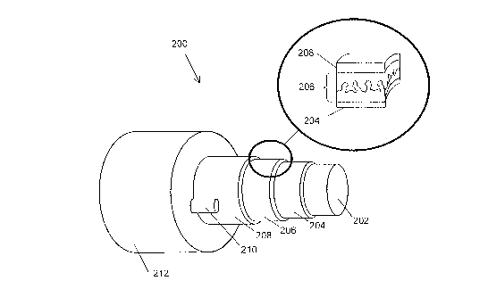
[0072] Figure 2 shows a representation of a photoactive fiber structure 200 in
accordance
with an embodiment of the invention. For clarity of illustration, Figure 2 may
not be to scale.
The photoactive fiber structure 200 may comprise a support,element 202; a
first electrode 204,
which may substantially surround the support element 202; an organic layer
206, which may
substantially surround the first electrode layer 204 and which comprises a
photoactive region; a
second electrode 208, which may substantially surround the organic layer 206;
and a auxiliary
conductor 210, which may be in electrical contact with some surface of the
transparent electrode
24
CA 02573498 2007-01-10
WO 2006/019576 PCT/US2005/023963
208. The photoactive fiber structure 200 in accordance with an embodiment of
the invention
may further comprise an outer layer 212.
[0073] In one embodiment, support element 202 may be fabricated of a flexible
solid
material. Examples may include an optical fiber, a telecommunications fiber,
and a solid nylon
strand. In one embodiment, the core may be a solid nylon strand. Other
materials are acceptable
without departing from the scope of the invention, and a wide variety of
dimensions may be used
depending upon the structural requirements of a particular application.
Together, support
element 202 and first electrode 204 comprise a "conductive core." Support
element 202 may be
conductive or non-conductive. In one embodiment, the conductive core may be a
single element,
without the need for a support element 202 separate from first electrode 204.
Preferable, such a
conductive core comprises a material that provides sufficient structural
properties and
conductivity. Metal wires are a preferred example of such a conductive core.
Whether or not
there is a separate support element 202, first electrode 204 may be comprised
of two or more
layers (such as, for example, a first layer of aluminum surrounded by a second
layer of lithium).
Examples of suitable conductive materials include silver, gold, copper, and
aluminum. Other
conductive materials may be used. Preferably, the conductive core is flexible.
[0074] In one embodiment, organic layer 206 may be a polymer or small-
molecular bulk
heterojunction coating. In one embodiment, the organic layer 206 may range in
thickness from
about 1 to 200 nm. Examples of polymer or small-molecular bulk heterojunction
coatings
include PCBM-nMDMO-PPV and CuPc-C60, respectively. As used herein,
PCBM is 6,6-phenyl-C61-Butyl acid-methylester
MDMO-PPV is poly(2-methoxy-5-(3',7'-dimethyloctyloxy)-1,4-phenylene-vinylene)
PPV is poly(1,4-phenylene-vinylene)
C60 is buckminsterfullerene
PtOEP is 2,3,7,8,12,13,17,18-Octaethyl-21 H,23H-porphine platinum (II) (also
platinum
octaethylporphyrin)
PTCBI is 3,4,9,1 0-perylenetetracarboxylic bis-benzimidazole
Other organic layers, such as a planar heterojunction layer or a mixed
heterojunction layer, as
well as other material combinations, that provide photogeneration may also be
selected without
departing from the scope of the invention.
CA 02573498 2007-01-10
WO 2006/019576 PCT/US2005/023963
[0075] In one embodiment, second electrode 208 may be transparent and comprise
a
polymer comprised of PEDOT-PSS. ITO is another preferred material. Preferably,
second
electrode 208 is transparent and flexible. Other transparent electrode
materials, whether metallic
or non-metallic, may also be selected without departing from the scope of the
invention.
[0076] In one embodiment, the outer layer 212 may be an optically transparent
nylon.
Other materials may also be used. Depending upon the amount of protection from
the
environment that is needed, and the amount of such protection that is provided
by other layers
such as second electrode 208, outer layer 212 may be omitted.
.[0077] In industrial practice it may be difficult to control the azimuth
orientation of a
photoactive fiber structure (similar to 200, Figure 2) in, for example, a
cloth within which the
fiber may be woven. In some cloth configurations, only 25% of a photoactive
fiber's surface
may be usefully exposed (compared to 50% in a conventional flat photovoltaic
cell). A second
electrode 208, comprised of, for example, ITO or PEDOT-PSS polymer, may be
used. However,
transparent electrodes, such as those comprised of ITO and PEDOT-PSS, may be
typically too
resistive to conduct current along a length greater than about 1 cm.
Accordingly, a auxiliary
conductor 210 may be applied to and may be in electrical contact with both
organic layer 206
and second electrode 208. The auxiliary conductor 210 may extract current over
the entire
length of the photoactive. fiber structure 200. In an embodiment, the
auxiliary conductor 210
may be comprised of, for example, sliver, gold, copper, or aluminum. The
auxiliary conductor
210 may be electrically coupled to second electrode 208, and may cover from
about 5 percent to
about 50 percent of an external surface of second electrode 208. Additionally,
while depicted in
Figure 2 as a solid wire, the auxiliary conductor may be any of at least a
metallic wire, a
metallized wire, a metallic ribbon, a metallized ribbon, and a metallic
coating. The auxiliary
conductor 210 may be wound about the photoactive fiber structure 200, or may
be applied in a
direction substantially parallel to the axis of support element 202. If wound,
it is preferred that
the duty cycle be low, such that the amount of surface covered by auxiliary
conductor 210 is
minimized, because auxiliary conductor 210 is not necessarily transparent and
it is desirable to
minimize the amount of light that is blocked by the auxiliary conductor. The
"duty cycle" is the
axial distance along a fiber in which auxiliary conductor 210 makes a complete
revolution. A
duty cycle of at least the circumference of the second electrode is preferred,
to avoid blocking
26
CA 02573498 2007-01-10
WO 2006/019576 PCT/US2005/023963
light from too much of the active region. For most materials that may be
desirable for use as
second electrode 208, and for most fiber dimensions, it is expected that
conduction in the axial
direction, and not conduction around the circumference of electrode 208, will
be the issue
addressed by auxiliary conductor 210, such that there may not be a significant
conductivity
benefit to a very small duty cycle. Where the solar fiber may be incorporated
into a product such
that the orientation of auxiliary conductor 210 is not readily controlled,
such as weaving into
certain cloths where only a part of the fiber is expected to be exposed to
light, it may be preferred
winding auxiliary conductor 210 with a duty cycle suffieciently low to avoid a
situation where a
fiber has an auxiliary conductor 210 is always oriented towards a light source
so as to block a
substantial fraction of the part of the fiber exposed to light. Furthermore;
in an embodiment, the
auxiliary conductor 210 may be a braid of electrical conductors (not shown)
surrounding second
electrode 208, where the degree of occlusion from the braid is preferably no
more than about 50
percent. Although Figure 3 illustrates an auxiliary conductor 210 that is
separated from organic
layer 206 by second electrode 208, such separation. is not necessary and
auxiliary conductor 210
may contact organic layer 206. For example, auxiliary conductor 210 may be
fabricated prior to
second electrode 208.
[0078] Figure 3 shows a representation of a photoactive fiber structure 300
similar to that
of the photoactive fiber structure of Figure 2, further including an exciton
blocking layer 320, in
accordance with an embodiment of the invention. The exciton blocking layer 320
may comprise
a non-photoactive layer disposed between organic layer 206 and second
electrode 208 such that
non-photoactive exciton blocking layer 320 is electrically coupled to each of
organic layer 206
and second electrode 208. Preferably, exciton blocking layer 320 is organic.
For ease of
illustration, exciton blocking layer 320 is shown only in the magnified
portion of Figure 3. Other
non-photoactive layers, preferably organic, may be be included in a
photoactive fiber structure,
between first electrode 204 and second electrode 208. For example, blocking
layers, smoothing
layers, and any other layers that are known or may become known to the art may
be incorporated
into the fiber structure.
[0079] One method of making a photoactive fiber structure 200 in accordance
with the
invention is coat a telecommunications fiber with ITO and then use vacuum
thermal evaporation
or dip-coating to deposit active organic layer(s). A conductor (similar to
210, Figure 2) may be
27
CA 02573498 2007-01-10
WO 2006/019576 PCT/US2005/023963
deposited using vacuum evaporation, after wlucn tne photoactive fiber may be
tested using
common electrical probing techniques.
[0080] The dimensions of a practical photoactive fiber are subject to its
architecture, and
both will be established simultaneously and somewhat iteratively. In general,
when considering
a generalized cylindrical device geometry as may be used in a flexible
photoactive fiber woven
into fabric, the overall fiber thickness may range from about 10-100 m,
including the outer
layer (similar to 212, Figure 2), while the active organic layers (e.g.,
organic layer 206) may
typically be only about 100 nm thick.
[00$1] The optical power absorbed by the active organic layers (e.g., organic
layer 206)
is given approximately by:
Pop, >_ (D= d - L (2)
where, (D, r2, and L denote the optical flux, fiber radius at the anode, and
uninterrupted fiber
length, respectively. The resulting total photocurrent is given by:
_ Popt rI pwr IPG ~ Vo, = FF (3)
where, r1p, FF, and Vo, denote the photovoltaic cell power efficiency, fill
factor, and open-
circuit voltage, respectively. (The power efficiency, rlpWr, accounts for any
additional absorption
losses to the incident solar flux in the structure.) The power produced in the
load circuit is:
P.d = Vd,bp ' I road =(0.0 5= FF = Vo,)- jPG (4)
where, 5% voltage drop was allowed along the length of the fiber and IPG=
Iioad during operation.
At the same time, Ohm's law dictates:
(0.05-FF=Vo~) p=L (5)
Iluna Acs
28
CA 02573498 2007-01-10
WO 2006/019576 PCT/US2005/023963
where, p is the resistivity of the anode (e.g., secona eiectrode 208 and/or
auxiliary conductor
210), while Ac5 z~ 7c=d=t is the cross-sectional area of the anode. Combining
equations (2) -(5)
obtains:
t > P Lz (D ?7p,vr (6)
05 FFZ=V2
[0082] If aluminum (p = 5=l0-gS2=m) were used as an inner conductor (similar
to 204,
Figure 2), and given 'qp, = 3%, FF = 0.5, Voc = 0.5V, an estimate of the
minimum thickness, in
meters, of the inner conductor (similar to 204, Figure 2) would be:
t _ 5=10-6 LZ (7)
where, L is also expressed in meters. Thus, a 5 m thick coating of Al can be
used if the current
is tapped out every 1 Ocm. This also sets the diameter of the conductor, viz.:
)r =d=t=ic=d~,14 (8)
where, daõ is the diameter of the auxiliary conductor, such as auxiliary
conductor 210, Figure 2.
Accordingly, from above, daõ = 30 m.
[0083] In one embodiment, the photoactive fiber structure 200, including the
auxiliary
conductor 210 may be wound together and then encapsulated by, for example, a
IO m thick
outer layer 212 to result in a slightly oblong cross-section photoactive fiber
structure that is about
110 m across its major diameter. This diameter may be suitable for typical
textile processing
equipment and incorporation into industrial and personal-use fabric.
[0084] It is believed that photoactive fiber structure in accordance with an
embodiment
of the invention may be fabricated at low-cost and incorporated into the high-
speed
manufacturing of textiles. One possible continuous fabrication sequence may be
to draw a metal
or a metallized nylon core through a melt containing a blend of photosensitive
polymer. The
photosensitive polymer may dry and phase separate, resulting in a bulk
heterojunction structure
surrounding the core. The core may then be coated with a conducting polymer
(e.g., PEDOT).
29
CA 02573498 2007-01-10
WO 2006/019576 PCT/US2005/023963
The conductor may be introduced and wound together with the photogenerating
core at a low
duty cycle, or may be linearly applied in a direction substantially parallel
to the axis of the core
of the photoactive fiber, to allow sufficient light absorption in the
photoactive fiber. Finally, the
entire photoactive fiber may be "fmished" by encapsulation in a transparent
plastic sheath or
other protective outer layer to help to protect it from mechanical (e.g.,
abrasive) and
environmental damage.
[0085] Ultimately, the feasibility of installed solar panels depends on the
cost of raw
materials, fabrication, module assembly, transport, and on-site installation.
While estimates of
the final cost of mass-manufactured photoactive fibers are only approximate,
it is expected to be
less than that of silicon photovoltaic cells. The mass of photoactive polymer
used in the
photoactive fiber can be calculated from the dimensions obtained above. A 1 m
long fiber will
require -10-5mg of dry photoactive polymer, and a lm2 swath of cloth woven
from the
photoactive fiber will use -0.1 g of it. Chemicals such as C60 are currently
available in large
quantities for <$30/gram (99% pure), and their price can be expected to drop
in the near future.
Nylon cloth is available to consumers at prices from $1 to $20 per m2,
depending on the weave,
treatment, and strength, and at substantially lower cost to large-volume
customers. A 3%
efficient lrn2 photovoltaic cell can generate on average 30 Watts of
electrical power. If the
photoactive fiber cost is in the range of technical synthetic-based fabric
price, the generated
power can cost between -$0.1 and $0.8 / Watt. A typical silicon-based solar
cell has a$3-4 /
Watt installed cost. Furthermore,. producing solar cells in the form of
mechanically robust
flexible fabric can greatly reduce installation costs compared to heavy and
bulky silicon
photovoltaic modules.
[0086] The nature of the polymers used to fabricate the photoactive fiber may
preferably
satisfy several optical, electrical, mechanical, and rheological requirements.
To maximize the
efficiency of a solar cell, the absorption spectrum of the photo-generating
layer should overlap-
the solar radiation spectrum as much as possible. Conjugated polymers
typically have band gaps
>2eV, which omits a significant portion of the incident solar radiation. The
structure and
composition of the active polymers can be modified to include the low-energy
part of the solar
spectrum using small-molecular-like side-branches and functional groups like
C60. See,
generally, Brabec, C.J., et al., Organic Photovoltaic Devices Produced From
Conjugated
CA 02573498 2007-01-10
WO 2006/019576 PCT/US2005/023963
Polynier/Methanofullerene Bulk Heterojunctions, Synthetic Metals, 2001, 121(1-
3): p. 1517;
Shaheen, S.E., et al., Low Band-Gap Polymeric Photovoltaic Devices, Synthetic
Metals, 2001,
121: p. 1583.
[00871 However, structural modification of the polymer will also affect its
melting
temperature, rheological behavior, and crystalline order. While polymer melt
rheology is a well-
studied topic, few studies exist dealing with rheology of polymers used in
photovoltaic cells;
many have been synthesized only in the last 5 years.
[0088] In addition to modifying the chemical structure of the photoactive
polymer, the
optical absorption may be improved ("sensitized") by doping low band-gap dye
molecules into
the host film. However, the excitons created on the dye molecules remain
trapped due to their
lower energy relative to the surrounding polymer matrix. Engineering a three-
phase morphology
on the nanometer scale, similar to that employed in a Gratzel cell may
surmount this limitation.
An amphiphilic dopant molecule may be mixed in with hydrophobic and
hydrophilic polymers,
such that upon annealing the amphiphilic dopant may create a third phase at
the boundary
between the two polymer phases. The net effect may be to absorb and
immediately dissociate a
low-energy exciton at the ternary interface.
[0089] Charge and exciton hopping between neighboring chains also limit the
output
current of a photovoltaic cell. The operating hypothesis for barrier coating
design is that
diffusion of chemical species (e.g. 02 and H20) into the photovoltaic cell
causes decomposition
of the photo- and electrically active compounds, accelerated by thermal and
optical stresses.
While moisture diffusion coefficients can be low in some polymeric materials,
oxygen diffusion
is more difficult to prevent. Metallic coatings are frequently used in some
applications (e.g. food
packaging, optical fiber coating, etc.), but they also block solar flux.
Instead, transparent oxide
(e.g. Ti02, Si02, and A1203) coatings can be used for the solar fiber. The
difficulty in using
oxide thin films as diffusion barriers in organic-based devices stems from a
processing and
application points of view. The deposition temperature for high-quality, dense
oxides is
typically high (>500 C), while the decomposition temperature of the organic
materials is
typically low (<500 C). The oxides are also brittle, with thermal expansion
coefficients different
from polymers, so that cracks are easily formed during handling and use.
Barrier coatings have
31
CA 02573498 2007-01-10
WO 2006/019576 PCT/US2005/023963
been developed, where alternating polymer and sputtered metal-oxide inorganic
thin films are
employed. See, e.g., Burrows, P.E., et al., Gas Permeation and Lifetime Tests
on Polymer-Based
Barrier Coatings, in SPIE Annual Meeting, 2000. The inorganic layers act to
block the diffusion
of chemical species harmful to the device, while the polymer interlayers act
to cushion and
mechanically decouple the oxide layers. Low-cost synthetic approaches, such as
sol-gel
synthesis of oxides may also be acceptable.
[0090] . For OLED embodiments, organic layer 206 may comprise the organic
layers of an
organic light emitting device. Such layers are illustrated (in a planar
fashion) in Figure 4, and
described in further detail above and below. An auxiliary conductor may be
used in an OLED
embodiment to provide current.
[0091] Hole transport layer 425 may include a material capable of transporting
holes.
Hole transport layer 430 may be intrinsic (undoped), or doped. Doping may be
used to enhance
conductivity. a-NPD and TPD are examples of intrinsic hole transport layers.
An example of a
p-doped hole transport layer is m-MTDATA doped with F4-TCNQ at a molar ratio
of 50:1, as
disclosed in United States Patent Application Publication No. 2002-0071963 Al
to Forrest et al.,
which is incorporated by reference in its entirety. Other hole transport
layers may be used
[0092] Emissive layer 435 may include an organic material capable of emitting
light
when a current is passed between anode 415 and cathode 460. Preferably,
emissive layer 435
contains a phosphorescent emissive material, although fluorescent
emissive'materials may also
be used. Phosphorescent materials are preferred because of the higher
luminescent efficiencies
associated with such materials. Emissive layer 435 may also comprise a host
material capable of
transporting electrons and / or holes, doped with an emissive material that
may trap electrons,
holes, and / or excitons, such that excitons relax from the emissive material
via a photoemissive
mechanism. Emissive layer 435 may comprise a single material that combines
transport and
emissive properties. Whether the emissive material is a dopant or a major
constituent, emissive
layer 435 may comprise other materials, such as dopants that tune the emission
of the emissive
material. Emissive layer 435 may include a plurality of emissive materials
capable of, in
combination, emitting a desired spectrum of light. Examples of phosphorescent
emissive
materials include Ir(ppy)3. Examples of fluorescent emissive materials include
DCM and
32
CA 02573498 2007-01-10
WO 2006/019576 PCT/US2005/023963
DMQA. Examples of host materials include Alq3, CBP and mCP. Examples of
emissive and
host materials are disclosed in U.S. Patent No. 6,303,238 to Thompson et al.,
which is
incorporated by reference in its entirety. Emissive material may be included
in emissive layer
435 in a number of ways. For example, an emissive small molecule may be
incorporated into a
polymer. This may be accomplished by several ways: by doping the small
molecule into the
polymer either as a separate and distinct molecular species; or by
incorporating the small
molecule into the backbone of the polymer, so as to form a co-polymer; or by
bonding the small
molecule as a pendant group on the polymer. Other emissive layer materials and
structures may
be used. For example, a small molecule emissive material may be present as the
core of a
dendrimer.
[0093] Many useful emissive materials include one or more ligands bound to a
metal
center. A ligand may be referred to as "photoactive" if it contributes
directly to the photoactive
properties of an organometallic emissive material. A "photoactive" ligand may
provide, in
conjunction with a metal, the energy levels from which and to which an
electron moves when a
photon is emitted. Other ligands may be referred to as "ancillary." Ancillary
ligands may
modify the photoactive properties of the molecule, for example by shifting the
energy levels of a
photoactive ligand, but ancillary ligands do not directly provide the energy
levels involved in
light emission. A ligand that is photoactive in one molecule may be ancillary
in another. These
definitions of photoactive and ancillary are intended as non-limiting
theories. Note that the term
"photoactive" as used herein generally means pertaining directly to the
absorption or emission of
light. The specific .meanings provided in the contexts of an OLED as opposed
to a
photosensitive device are contextual applications of the general definition;
[00941 Electron transport layer 440 may include a material capable of
transporting
electrons. Electron transport layer 440 may be intrinsic (undoped), or doped.
Doping may be
used to enhance conductivity. Alq3 is an example of an intrinsic electron
transport layer. An
example of an n-doped electron transport layer is BPhen doped with Li at a
molar ratio of 1:1, as
disclosed in United States Patent Application Publication No. 2002-0071963 Al
to Forrest et al.,
which is incorporated by reference in its entirety. Other electron transport
layers may be used.
33
CA 02573498 2007-01-10
WO 2006/019576 PCT/US2005/023963
100951 The charge carrying component of the electron transport layer may be
selected
such that electrons can be efficiently injected from the cathode into the LUMO
(Lowest
Unoccupied Molecular Orbital) energy level of the electron transport layer.
The "charge carrying
component" is the material responsible for the LUMO energy level that actually
transports
electrons. This component may be the base material, or it may be a dopant. The
LUMO energy
level of an organic material may be generally characterized by the electron
affinity of that
material and the relative electron injection efficiency of a cathode may be
generally
characterized in tenns of the work function of the cathode material. This
means that the preferred
properties of an electron transport layer and the adjacent cathode may be
specified in terms of the
electron affinity of the charge carrying component of the ETL and the work
function of the
cathode material. In particular, so as to achieve high electron injection
efficiency, the work
function of the cathode material is preferably not greater than the electron
affinity of the charge
carrying component of the electron transport layer by more than about 0.75 eV,
more preferably,
by not more than about 0.5 eV. Similar considerations apply to any layer into
which electrons are
being injected.
[0096] Blocking layers in an OLED may be used to reduce the number of charge
carriers
(electrons or holes) and / or excitons that leave the emissive layer. An
electron blocking layer
430 may be disposed between emissive layer'435 and the hole transport layer
425, to block
electrons from leaving emissive layer 435 in the direction of hole transport
layer 425. Similarly,
a hole blocking layer 440 may be disposed between emissive layerl35 and
electron transport
layer 445-, to block holes from leaving emissive layer 435 in the direction of
electron transport
layer 440. Blocking layers may also be used to block excitons from diffusing
out of the emissive
layer. The theory and use of blocking layers is described in more detail in
United States Patent
No. 6,097,147 and United States Patent Application Publication No. 2002-
0071963 Al to Forrest
et al., which are incorporated by reference in their entireties.
[0097] As used herein, and as would be understood by one skilled in the art,
the term
"blocking layer" means that the layer provides a barrier that significantly
inhibits transport of
charge carriers and/or excitons through the device, without suggesting that
the layer necessarily
completely blocks the charge carriers and/or excitons. The presence of such a
blocking layer in a
device may result in substantially higher efficiencies as compared to a
similar device lacking a
34
CA 02573498 2007-01-10
WO 2006/019576 PCT/US2005/023963
blocking layer. Also, a blocking layer may be used to confine emission to a
desired region of an
OLED.
[0098] Generally, injection layers are comprised of a material that may
improve the
injection of charge carriers from one layer, such as an electrode or an
organic layer, into an
adjacent organic layer. Injection layers may also perform a charge transport
function. In device
400, hole injection layer 420 may be any layer that improves the injection of
holes from anode
415 into hole transport layer 425. CuPc is an example of a material that may
be used as a hole
injection layer from an ITO anode 415, and other anodes. In device 400,
electron injection layer
450 may be any layer that improves the injection of electrons into electron
transport layer 445.
LiF / Al is an example of a material that may be used as an electron injection
layer into an
electron transport layer from an adjacent layer. Other materials or
combinations of materials
may be used for injection layers. Depending upon the configuration of a
particular device,
injection layers may be disposed at locations different than those shown in
device 400. More
examples of injection layers are provided in U.S. Patent Application Serial
No. 09/931,945 to Lu
et al., which is incorporated by reference in its entirety. A hole injection
layer may comprise a
solution deposited material, such as a spin-coated polymer, e.g., PEDOT:PSS,
or it .may be a
vapor deposited small molecule material, e.g., CuPc or MTDATA.
[0099] A hole injection layer (HIL) may planarize or wet the anode surface so
as to
provide -efficient hole injection from the anode into the hole injecting
material. A hole injection
layer may also have a charge carrying component having HOMO (Highest Occupied
Molecular
Orbital) energy levels that favorably match up, as defined by their herein-
described relative
ionization potential (IP) energies, with the adjacent anode layer on one side
of the HIL and the
hole transporting layer on the opposite side of the HIL. The "charge carrying
component" is the
material responsible for the HOMO energy level that actually transports holes.
This component
may be the base material of the HIL, or it may be a dopant. Using a doped HIL
allows the
dopant to be selected for its electrical properties, and the host to be
selected for morphological
properties such as wetting, flexibility, toughness, etc. Preferred properties
for the HIL material
are such that holes can be efficiently injected from the anode into the HIL
material. In particular,
the charge carrying component of the HIL preferably has an IP not more than
about 0.7 eV
greater that the IP of the anode material. More preferably, the charge
carrying componeiit has an
CA 02573498 2007-01-10
WO 2006/019576 PCT/US2005/023963
IP not more than about 0.5 eV greater than the anode material. Similar
considerations apply to
any layer into which holes are being injected. HIL materials are further
distinguished from
conventional hole transporting materials that are typically used in the hole
transporting layer of
an OLED in that such HIL materials may have a hole conductivity that is
substantially less than
the hole conductivity of conventional hole transporting materials. The
thickness of the HIL of
the present invention may be thick enough to help planarize or wet the surface
of the anode layer.
For example, an HIL thickness of as little as 10 mu may be acceptable for a
very smooth anode
surface. However, since anode surfaces tend to be very rough, a thickness for
the HIL of up to 50
nm may be desired in some cases.
[0100] A protective layer may be used to protect underlying layers during
subsequent
fabrication processes. For example, the processes used to fabricate metal or
metal oxide top
electrodes may damage organic layers, and a protective layer may be used to
reduce or eliminate
such damage. In device 400, protective layer 455 may reduce damage to
underlying organic
layers during the fabrication of cathode 460. Preferably, a protective layer
has a high carrier
mobility for the type of carrier that it transports (electrons in device 400),
such that it does not
significantly increase the operating voltage of device 400. CuPc, BCP, and
various metal
phthalocyanines are examples of materials that may be used in protective
layers. Other materials
or combinations of materials may be used. The thickness of protective layer
455 is preferably
thick enough that there is little or no damage to underlying layers due to
fabrication processes
that occur after organic protective layer 460 is deposited, yet not so thick
as to significantly
increase the operating voltage of device 400. Protective layer 455 may be
doped to increase its
conductivity. For example, a CuPc or BCP protective layer 460 may be doped
with Li. A more
detailed description of protective layers may be found in U.S. Patent
Application Serial No.
09/931,948 to Lu et al., which is incorporated by reference in its entirety.
[0101] Unless otherwise specified, any of the layers of the various
embodiments may be
deposited by any suitable method. For the organic layers, preferred methods
include thermal
evaporation, ink-jet, such as described in U.S. Patent Nos. 6,013,982 and
6,087,196, which are
incorporated by reference in their entireties, organic vapor phase deposition
(OVPD), such as
described in U.S. Patent No. 6,337,102 to Forrest et al., which is
incorporated by reference in its
entirety, and deposition by organic vapor jet printing (OVJP), such as
described in U.S. Patent
36
CA 02573498 2007-01-10
WO 2006/019576 PCT/US2005/023963
Application No. 10/233,470, which is incorporated by reference in its
entirety. Other suitable
deposition methods include spin coating and other solution based processes.
Solution based
processes are preferably carried out in nitrogen or an inert atmosphere. For
the other layers,
preferred methods include thermal evaporation. Preferred patterning methods
include deposition
through a mask, cold welding such as described in U.S. Patent Nos. 6,294,398
and 6,468,819,
which are incorporated by reference in their entireties, and patterning
associated with some of
the deposition methods such as ink-jet and OVJD. Other methods may also be
used. The
materials to be deposited may be modified to make them compatible with a
particular deposition
method. For example, substituents such as alkyl and aryl groups, branched or
unbranched, and
preferably containing at least 3 carbons, may be used in small molecules to
enhance their ability
to undergo solution processing. Substituents having 20 carbons or more may be
used, and 3-20
carbons is a preferred range. Materials with asymmetric structures may have
better solution
processibility than those having symmetric structures, because asymmetric
materials may have a
lower tendency to recrystallize. Dendrimer substituents may be used to enhance
the ability of
small molecules to undergo solution processing.
.[0102] The molecules disclosed herein may be substituted in a number of
different ways
without departing from the scope of the invention. For example, substituents
may be added to a
compound having three bidentate ligands, such that after the substituents are
added, one or more
of the bidentate ligands are linked together to form, for example, a
tetradentate or hexadentate
ligand. Other such linkages may be formed. It is believed that this type of
linking may increase
stability relative to a similar compound without linking, due to what is
generally understood in
the art as a "chelating effect."
[0103] Devices fabricated in accordance with embodiments of the invention may
be
incorporated into a wide variety of consumer products, including flat panel
displays, computer
monitors, televisions, billboards, lights for interior or exterior
illuminatiorn and / or signaling,
heads up displays, fully transparent displays, flexible displays, laser
printers, telephones, cell
phones, personal digital assistants (PDAs), laptop computers, digital cameras,
camcorders,
viewfinders, micro-displays, vehicles, a large area wall, theater or stadium
screen, or a sign.
Various control mechanisms may be used to control devices fabricated in
accordance with the
present invention, including passive matrix and active matrix. Many of the
devices are intended
37
CA 02573498 2007-01-10
WO 2006/019576 PCT/US2005/023963
for use in a temperature range comfortable to humans, such as 18 degrees C.to
30 degrees C, and
more preferably at room temperature (20 - 25 degrees C)
[0104] Although the present invention is described with respect to particular
examples
and preferred embodiments, it is understood that the present invention is not
limited to these
examples and embodiments. The present invention as claimed may therefore
include variations
from the particular examples and preferred embodiments described herein, as
will be apparent to
one of skill in the art.
38