Note: Descriptions are shown in the official language in which they were submitted.
CA 02573935 2012-12-18
1
METHOD FOR PRODUCING A THREE-DIMENSIONAL PHOTONIC CRYSTAL
USINGADOUBLEINVERSIONTECHNIQUE
This application claims the priority of DE
2004 037 950.5.
5 The invention relates to a process for producing a
three-dimensional photonic crystal which consists of a
material with high refractive index.
Photonic crystals, which date back to E. Yablonovitch,
Phys. Rev. Lett., Volume 58, page 2059-2062, 1987, and
10 S. John, ibid., page 2486-2489, 1987, are periodically
structured dielectric materials which constitute the
optical analog of semiconductor crystals and thus
enable the production of integrated photonic circuits.
Extended photonic band gaps, which, according to K.-M.
Ho, C.T. Chan, and C.M. Soukoulis, Phys. Rev. Lett.
Volume 65, page 3152-3155, 1990, can theoretically have
up to 25% of the central frequency of silicon at
2.6 m, can be produced with photonic crystals which
have a diamond structure instead of a face-centered
cubic structure.
Layer structures in particular are, according to K.-M.
Ho, C.T. Chan, C.M. Soukoulis, R. Biswas, and M.
Sigalas, Solid State Comm., Volume 89, page 413-416,
1994, and E. zbay et al, Phys. Rev. B, Volume 50, page
1945-1948, 1994, obtainable via microfabrication
processes. Recently, S.Y. Lin et al., Nature, 'Volume
CA 02573935 2012-12-18
la
394, page 251-253, 1998, S. Noda et al., Science,
Volume 289, page 604-606, 2000, and K. Aoki et al.,
Nature Materials, Volume 2, page 117-121, 2003, have
produced photonic crystals for infrared frequencies by
combining planar semiconductor microstructuring
CA 02573935 2007-01-15
- 2 -
processes for individual layers with sophisticated
alignment and stacking processes in order to configure
a three-dimensional photonic crystal from the layers.
This allows incorporation of functional elements by
controlled changes in individual layers. However,
stacking had to date only been successful for a few
layers, which leads to high coupling between the
conduction modes in the photonic crystal and the loss
modes in the surrounding material, as a result of which
the performance of the functional elements is
restricted.
Therefore, M. Campbell et al., Nature, Volume 404, page
53-56, 2000, and Y.V. Miklyaev et al., Appl. Phys.
Lett., Volume 82, page 1284-1286, 2003, moved to the
production of extended three-dimensional photonic
crystals of high quality in photoresist layers by means
of holographic lithography. Here, the thickness of the
photonic crystals is in principle restricted only by
the thickness of the photoresist layer and its
absorption. Holographic lithography enables the
provision of defect-free layers with a thickness of a
few lOs unit cells with an expansion of a few mm2, this
process having great flexibility with regard to the
contents of the unit cell. However, this multibeam
interference process only allows the production of
strictly periodic structures.
Therefore, a second complementary process is required
to write functional elements, for example waveguides or
microcavity structures, into the interior of a photonic
crystal which has been produced by holographic
lithography. Particularly suitable for this purpose is
the so-called direct laser writing (DLW) by multiphoton
polymerization in the photosensitive material, known
from S. Kawata, H.-B. Sun, T. Tanaka and K. Takada,
Nature, Volume 412, page 697-698, 2001.
CA 02573935 2012-12-18
3
In this method, a photoresist is illuminated by means
of a laser whose frequency is below the single-photon
polymerization threshold of the photoresist. When this .
laser is focused onto the interior of the photoresist,
the light intensity within a small volume at the focal
point can exceed the threshold for multiphoton
polymerization. Size and shape of these so-called
voxels depend upon the isointensity surfaces, i.e.
isophotes, the microscope lens used and the
illumination threshold for multiphoton polymerization
in the photosensitive material. Using this process, S.
Kawata et al. have to date been able to produce voxels
with a size down to 120 nm with illumination at 780 nm.
In conjunction with holographic lithography, direct
laser writing offers a rapid and precise way of
providing functional elements in photonic crystals.
However, the introduction of materials with high
refractive index is not possible thereby, since high
temperatures for the coating and high chemical
reactivity of the precursor substances for known
coating processes, for example chemical vapor
deposition (CVD), destroy the existing structures.
Proceeding from this, it is an object of the present
invention to propose a process for producing a photonic
crystal which consists of a material with high
refractive index, said process not having the
disadvantages and restrictions mentioned.
CA 02573935 2012-12-18
3a
This object is achieved by a process for producing a photonic crystal having a
complete band gap which consists of a material having high refractive index,
comprising the following process steps:
a) providing a photonic crystal which consists of a cross-linked polymer
and through whose surface there are empty interstitial sites, wherein the
photonic
crystal which consists of a cross-linked polymer is applied to a first
substrate,
b) introducing a filler into the interstitial sites, so that a network of the
filler
is formed therein, and performing one of:
1) applying a second substrate to the surface of the photonic
crystal which consists of a cross-linked polymer after the network of the
filler
has formed in the interstitial sites of the photonic crystal; and
2) removing the uppermost layer from the filler by means of
reactive ion etching,
c) removing the cross-linked polymer, which forms cavities in the network
formed from the filler,
d) introducing a material with high refractive index into the cavities, so
that a structure of the material with high refractive index is formed therein,
and
e) removing the filler, which leaves the structure of the material with high
refractive index, which can be removed as the photonic crystal having a
complete
band gap which consists of a material with high refractive index.
The process according to the invention constitutes a
double inversion process, i.e. the original polymeric
photonic crystal is first converted to a spatially
inverse structure which in turn, as a result of a
second inversion, forms a photonic crystal which
CA 02573935 2007-01-15
- 4 -
consists of the desired material with high refractive
index. The starting materials are in each case removed
with suitable processes.
The starting point of the process according to the
invention is a three-dimensional photonic crystal which
consists of a polymer and is provided according to
process step a). To this end, according to the prior
art, preference is given to applying a polymer or a
polymerizable monomer by means of spin-coating to a
first substrate made of glass, silicon or a polymer.
In a particularly embodiment, this polymer or
polymerizable monomer covers the entire first substrate
and is then, if appropriate, completely polymerized.
Only then is a second layer of the polymer or
polymerizable monomer applied thereto.
Subsequently, a polymeric photonic crystal with the
desired crystal structure is produced from the polymer,
preferably by means of holographic lithography, direct
laser writing or a combination of the two processes.
Such a photonic crystal has a surface area by which a
lattice with empty interstitial sites is defined.
The first inversion, i.e. the conversion of the
original polymeric photonic crystal to a spatially
inverse structure, is effected by, according to process
step b), introducing a suitable filler into the empty
interstitial sites in such a way that a network is
formed from the filler at the interstitial sites.
In a preferred embodiment, a precursor substance of the
filler is introduced into the initially empty
interstitial sites, where it is deposited onto the
surface of the polymeric photonic crystal. The amount
of precursor substance is selected such that it fills a
predetermined volume fraction of the empty
interstitials which is sufficient to form a layer from
CA 02573935 2007-01-15
- 5 -
the filler on the surface of the polymeric photonic
crystal, which constitutes an interconnected network of
filler in the previously empty interstitial sites of
the polymeric photonic crystal.
In a particularly preferred embodiment, silicon
tetrachloride SiC14 is used as the precursor substance
and then converted to the desired silicate filler Si02
in a conventional manner.
Since, in process step b), the entire polymer structure
present is covered with the filler material, direct
removal of the polymer in process step c) by thermal
decomposition or plasma etching is generally not
possible. Thermal decomposition leads to generation of
gaseous products within the closed structure and hence
to their explosive decomposition; plasma etching does
not work since the reactive gases cannot reach the
polymer to be decomposed through the filler material.
In a particular embodiment, this difficulty is
circumvented by, before the removal of the polymer,
applying a second substrate, which preferably consists
of glass or another material which is stable at high
temperatures but can be released in strong acids, to
the structure, preferably by means of a sol-gel process
or an adhesive (high-performance adhesive). In the
thermal composition which follows, the gaseous products
separate the first substrate from the structure which,
in this embodiment, rests on a thin polymer layer.
After this separation, sufficient removal channels have
been opened for the gaseous decomposition products of
the polymer from the interior of the structure, so that
they can escape without destroying the structure.
In an alternative embodiment, this difficulty is
circumvented by removing the uppermost layer from the
filler (silicate) by means of reactive ion etching.
This too opens up sufficient removal channels for the
CA 02573935 2007-01-15
- 6 -
gaseous reaction products of the polymer from the
interior of the structure, so that they can escape
without destroying the structure.
When, in process step c), the polymer of which the
original photonic crystal consisted has been removed,
preferably by means of plasma etching or thermal
decomposition, cavities form in the network formed from
filler.
The desired photonic crystal is now produced from the
structure thus formed by a second inversion. To this
end, in process step d), the selected material with
high refractive index, i.e. high dielectric constant,
is introduced into the cavities formed beforehand, so
that a structure of the material with high refractive
index forms therein. The material with high refractive
index is preferably applied layer by layer to the inner
surfaces of the cavities in the filler up to the
desired thickness.
The materials with high refractive index used are
preferably the semiconductors silicon, also provided
with various n- or p-dopants, germanium or an SixGel-x
alloy. Silicon may itself be amorphous,
nanocrystalline, polycrystalline or monocrystalline,
hydrogenated nanocrystalline silicon (nc-Si:H) being a
particularly preferred material. In addition, II-V, II-
VI, I-VII, IV-VI semiconductors including their n- or
p-doped variants, or metals with high refractive index,
for example silver (Ag), gold (Au), tungsten (W),
iridium (Ir) or tantalum (Ta), are equally suitable.
Before, finally, in process step e), the photonic
crystal which consists of the material with high
refractive index is removed, once the filler has been
removed, the structure, preferably by means of an
optically transparent adhesive (optical adhesive), is
secured to a third substrate which is inert toward
CA 02573935 2007-01-15
- 7 -
strong acids, for example hydrogen fluoride (HF) or
hydrochloric acid (HC1), and preferably consists of a
polymer of optical quality. Without this step, there is
the risk of losing a photonic crystal with low
dimensions in the acid after the removal of the filler
material and the substrate.
The removal of the filler, which is preferably effected
by means of a strong acid, for example hydrogen
fluoride (HF) or hydrochloric acid (HC1), brings about,
if appropriate, the removal of the original substrate
and the formation of the desired three-dimensional
photonic crystal of material with high refractive
index, whose structure is similar or identical to the
polymeric three-dimensional photonic crystal provided
in process step a). The crystal lattice of the photonic
crystal thus obtained may, for example, have a cubic
face-centered (fcc), a simple cubic (sc), a slanted
pore, a diamond or a quadratic spiral structure.
The process according to the invention enables the
production of three-dimensional photonic crystals with
high dielectric contrast. These may have any structures
and topologies which can be produced by means of
holographic lithography, direct laser writing or a
combination of the two processes. This at the same time
allows functional photonic devices based on three-
dimensional photonic crystals to be produced without
further process steps. Photonic crystals produced by
the process according to the invention have complete
band gaps in the region of telecommunications
wavelengths.
The invention is illustrated hereinafter with reference
to working examples and the figures. The figures show:
Fig. 1 Schematic illustration of the process steps
for two embodiments of the process.
CA 02573935 2007-01-15
- 8 -
Fig. 2 Scanning electron micrograph of a double-
inverted silicon structure.
Fig. 3 Calculated photonic band structure of a
double-inverted silicon structure.
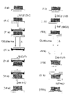
Fig. 1 shows a schematic of the process steps I-VII for
two embodiments of the process designated by a and b:
Ia, lb Starting point: substrate (glass) with
applied polymeric photonic crystal,
produced with multiphonon or holographic
polymerization (process step a).
ha, IIb Filling of the interstitial sites of the
polymeric photonic crystal by means of CVD
of 5i02 (process step b).
IIIa Application of a further substrate to the
surface of the crystal composed of polymer
and Si02.
IIIb Removal of the excess 5i02 by means of
reactive ion etching (RIE).
IVa Removal of the original substrate and of
the polymeric photonic crystal by means of
heating (A) or 02 plasma etching (process
step c).
IVb Removal of the polymeric photonic crystal
by means of heating (A) or 02 plasma etching
(process step c).
Va, Vb Layer-by-layer introduction of silicon or
another material with high refractive index
into the interstitial sites of the photonic
structure inverted with Si02 (process
step d).
CA 02573935 2007-01-15
- 9 -
VIa, VIb Application of a further substrate to the
surface of the crystal composed of silicon
and Si02.
VIIa, VIIb Removal of the Si02 by wet-chemical etching
in a strong acid (e.g. HF or HC1) leads to
a photonic crystal composed of silicon or
composed of another material with high
refractive index, whose cavities (pores)
are filled by the surrounding atmosphere
(air) (process step e).
Depending on the number of layers introduced in steps
(II) and (V), photonic crystals with different
topologies can be produced.
To perform the process according to the invention, in
process step a), the starting point provided in each
case is a polymeric photonic crystal which has been
introduced by means of direct laser writing into a
photoresist composed of EPON SU-8 and had been applied
to a glass substrate which had optionally been covered
with photopolymerized EPON SU-8.
Subsequently, Si02 was introduced layer by layer into
the polymeric photonic crystal by means of chemical
vapor deposition (CVD), for example via the SiC14
precursor substance, until complete filling of the
polymer structure had been achieved (process step b).
Thereafter, two alternative embodiments which comprise
process step c) were performed:
(a) The sample was rotated and applied to a further
substrate which serves for transfer. In this
working example, a glass substrate with a rough
surface was selected for this purpose. The
adhesive used was, for example, a sol-gel mixture
CA 02573935 2007-01-15
- 10 -
of Si02 (silicate) which had been produced with
TMOS and a commercially available suspension of
silicate colloid particles in water. Commercially
available high-temperature-resistant adhesives
have likewise been used successfully. The original
glass substrate and the polymeric photonic crystal
were removed by 02 plasma etching over 20 hours or
by thermal decomposition of the polymer at 450 C
over 6 hours. A combination of the two processes
was likewise found to be advantageous.
In this embodiment, the first substrate should
preferably point downward, in order to be removed
by gravity owing to lack of adhesion as soon as
the polymer has decomposed. Otherwise, there is a
risk that the first substrate and the silicate-
inverted structure sinter together at the high
temperatures which occur, as a result of which
later introduction of highly refractive material
is no longer possible.
(b) The Si02 structure which had grown above the
surface of the photonic crystal was removed by
means of controlled reactive ion etching. The
original polymeric photonic crystal was removed by
02 plasma etching over 20 hours or by thermal
decomposition of the polymer at 450 C over 6
hours. A combination of the two processes was
likewise found to be successful.
As a result, a mirror image of the original polymeric
photonic crystal was obtained, which withstands the
high temperatures which are required for the pyrolysis
of the disilane (Si2'H6) precursor substance during the
layer by layer application of hydrogenated amorphous
silicon (a-Si:H) during process step d) by chemical
vapor deposition (CVD).
CA 02573935 2007-01-15
- 11 -
The pressure was kept constant at 320 Pa (2.4 Torr),
while the coating rate and the optical properties of
the film were laid down by the temperature of the
substrate, which can vary between 340 and 430 C.
In order to obtain hydrogenated nanocrystalline silicon
(nc-Si:H), the sample was then treated thermally in a
nitrogen atmosphere with 5% hydrogen at 600 C for 20
hours.
Subsequently, the sample was rotated and placed onto a
polymethyl methacrylate (PMMA) substrate of high
optical quality or another substrate which does not
react in strong acids and which meets the optical
requirements, onto which a thin adhering film of a
photopolymerizable polymer of high optical quality has
been applied. In order to achieve good adhesion, the
sample was then placed under an ultraviolet lamp for 5-
10 minutes.
Finally, in process step e), the silicate substrate and
the photonic crystal were etched completely in a
solution composed of 10% by weight of aqueous hydrogen
fluoride (HF) and 12% by weight of aqueous hydrochloric
acid (HC1).
Fig. 2 shows a scanning electron micrograph (SEM) of an
inverted silicon woodpile structure produced in
accordance with the invention in high magnification. It
becomes clear that the replica has been completely
inverted, has been distributed homogeneously over the
entire volume of the original polymer structure and has
a smooth surface.
To analyze the properties of the photonic crystals
produced in accordance with the invention, band
structure calculations were performed on the basis of
the plane-wave expansion method.
CA 02573935 2007-01-15
- 12 -
To this end, the lattice was modeled as fixed
rectangular silicon beams which are arranged in a
classical woodpile structure against a background of
air. A value of n = 3.45 for the refractive index of
nc-Si:H was used owing to the agreement of experimental
findings in thin films on silicate with literature
data.
The result of the calculations for this structure can
be found in Fig. 3. This structure has a band gap of
23% (width of the band gap based on the center
frequency) at a frequency of 2.6 pm. These band
structure calculations prove the presence of a
completely photonic band gap with a pronounced
structure.