Note: Descriptions are shown in the official language in which they were submitted.
CA 02574028 2007-01-16
WO 2006/011650 PCT/JP2005/014164
1
DESCRIPTION
ACOUSTIC WAVE SENSOR
Technical Field
The present invention relates to an acoustic wave sensor
utilizing acoustic wave for detecting a distance to an object and/or an
orientation where the object is located.
Background Art
As for such a kind of acoustic wave sensor, for example,
Japanese Laid-Open Patent Publication No. 2002-156451 discloses an
acoustic wave sensor of reflected wave formula. In the acoustic
wave sensor of reflected wave formula, compressional wave such as
ultrasonic wave is intermittently transmitted from a wave transmitter
having a wave transmitting device to a medium, and reflected wave
reflected by an object is received by a wave receiver having a wave
receiving device. A distance to the object and an orientation where
the object is located is detected on the basis of a time difference from
the transmission of the compressional wave to the receiving of the
reflected wave.
On the other hand, for example, Japanese Laid-Open Patent
Publication No. 2003-279640 discloses an acoustic wave sensor of
direct wave formula. In the acoustic wave sensor of direct wave
formula, compressional wave is intermittently transmitted from a
wave transmitter to a medium, and a distance to the wave transmitter
CA 02574028 2007-01-16
WO 2006/011650 PCT/JP2005/014164
2
and an orientation where the wave transmitter is located are detected
on the basis of a time difference from the transmission of the
compressional wave to the receiving of the compressional wave by a
wave receiver.
As for the application of the acoustic wave sensor, an
ultrasonic level gauge, a back sonar in-vehicle, and so on are
provided as examples which propagate the ultrasonic wave in the air.
Alternatively, a sonar, a fish detector, and so on are provided as
examples which propagate the ultrasonic wave in the underwater.
Furthermore, an ultrasonic flaw detector, an ultrasonic CT, and so on
are provided as examples which propagate the ultrasonic wave in a
structure.
In the above-mentioned acoustic wave sensor, the wave
receiver has a plurality of wave receiving devices which are arranged
on the same plane for receiving the acoustic waves transmitted from
the wave transmitter. When an orientation of arrangement of the
wave receiving devices forms a predetermined angle (except cases of
right angle and parallel) with respect.to an arrival orientation of the
acoustic waves corresponding to the orientation where the object is
located, time differences occur in times when the wave receiving
devices respectively receive the acoustic waves owing to an
arrangement pitch of the wave receiving devices and the
predetermined angle. Therefore, it is possible to detect the arriving
direction of the acoustic wave, that is, the direction where the object
is located by detecting phase differences between two signals
CA 02574028 2007-01-16
WO 2006/011650 PCT/JP2005/014164
3
outputted from adjoining two wave receiving devices when they
receive the acoustic waves.
In the conventional acoustic wave sensors, piezoelectric
devices are widely used as the wave transmitting device for
transmitting acoustic wave in the air and the wave receiving devices
for converting received acoustic waves to wave receiving signals of
electric signals. In the acoustic wave sensor which uses
piezoelectric devices for both of the wave transmitting device and the
wave receiving devices, frequency of acoustic wave transmitted from
the wave transmitting device is generally set in a frequency near to
resonance frequency of the wave transmitting device and the wave
receiving devices for a purpose of increasing acoustic pressure of the
acoustic wave to be transmitted and sensitivity for sensing acoustic
wave in each wave receiving device.
However, in the acoustic wave sensor using the piezoelectric
device as the wave transmitting device, reverberation component due
to resonance of the wave transmitting device is included in the
acoustic wave transmitted from the wave transmitting device. In
addition, reverberation component due to resonance of the wave
receiving device is included in the wave receiving signal outputted
from each wave receiving device in the acoustic wave sensor using
the piezoelectric devices as the wave receiving devices. In the
acoustic wave sensor using the piezoelectric devices for both of the
wave transmitting device and the wave receiving devices,
reverberation components due to resonances of both devices are
CA 02574028 2007-01-16
WO 2006/011650 PCT/JP2005/014164
4
included.
A Q factor (mechanical quality factor Qm) of resonance
characteristic of the piezoelectric device is generally larger than 100.
Thus, when the wave transmitting device of the piezoelectric device is
intermittently driven, the acoustic wave generated by the wave
transmitting device becomes vibration wave as shown in FIG. 20.
The larger the value of the Q factor of the resonance characteristic
becomes, the longer a term Ti necessary for becoming the amplitude
of the vibration waveform to the greatest, and the longer a term
(reverberation term) T2 necessary for converging the reverberation
oscillation become. Thus, the term from the transmission of the
acoustic wave to the receiving of the acoustic wave becomes shorter.
Therefore, for example, in the acoustic wave sensor for
detecting a distance to an object, it is impossible to detect the distance
to the object with respect to the object positioned within a
predetermined distance from the wave receiving devices. Hereupon,
when a temperature is designated by a symbol "t" ( C), acoustic
velocity "c" (m/s) of acoustic wave is calculated by the equation
c=331.5+0.6t. For example, when the temperature is assumed as 14
degrees Celsius, acoustic velocity c is 340 (m/s). In this case,
acoustic wave advances only 34 cm per 1 ms. When assuming the
reverberation term T2 of the vibration waveform of the acoustic wave
transmitted from the wave transmission device is 2 ms, it is
impossible to.measure the distance to the object located at a position
within 34 cm from the wave receiving devices.
CA 02574028 2007-01-16
WO 2006/011650 PCT/JP2005/014164
As just described, in the acoustic wave sensor using the
piezoelectric device as the wave transmitting device, since a dead
zone caused by the reverberation component included in the acoustic
wave transmitted from the wave transmitting device is longer, a
distance to an object relatively near to the wave receiving devices
cannot be detected.
Furthermore, it is assumed that two objects are located in
relatively shorter distances to the acoustic wave sensor using the
piezoelectric devices as the wave transmitting device and the wave
receiving devices. Reflected wave reflected by one object may
arrive at the wave receiving devices of the acoustic wave sensor while
reflected wave reflected by the other object is received by the wave,
receiving devices. In such a case, it is difficult to distinguish
between the reflected waves from these two objects on the basis of the
wave receiving signals outputted from the wave receiving devices.
In other words, the acoustic wave sensor using piezoelectric
devices for the wave transmitting device and the wave receiving
devices has a long dead zone caused by the reverberation component
included in the acoustic wave transmitted from the wave transmitting
device and the reverberation component included in the wave
receiving signals outputted from the wave receiving devices. Thus,
even in an area where the distance and/or orientation of the object can
be detected by the acoustic wave sensor, when differences among
distances from the acoustic wave sensor to a plurality of the objects
are smaller, the distances to the objects may not be detected.
CA 02574028 2007-01-16
WO 2006/011650 PCT/JP2005/014164
6
Accordingly, it is desired to improve angular resolution of the
acoustic wave sensor. In addition, the wave transmitting device and
the wave receiving devices used in the acoustic wave sensor have
characteristics that the Q factor of resonance characteristic becomes
larger as the angular resolution becomes lower.
Furthermore, it is possible to constitute a position detecting
system for detecting position information of an object to be detected
with using the above acoustic wave sensor. For example, according
to the above Japanese Laid-Open Patent Publication No. 2003-279640,
a position detecting system, which comprises ultrasonic wave
transmitters respectively provided on a plurality of migration objects,
at least three ultrasonic wave receivers respectively provided in
predetermined areas on a ceiling of a building, and a processor for
obtaining position information of the migration objects on the basis of
a term from a time when the ultrasonic wave transmitter transmits the
ultrasonic wave to a time when the ultrasonic wave receiver receives
the ultrasonic wave, is proposed.
In such a position detecting system, the ultrasonic wave
receivers are,provided one by one in every predetermined areas on the
ceiling of the building, so that it is necessary to install the ultrasonic
wave receivers in at least three places so as to obtain the positioning
information of the object to be detected (migration object) in the
processor. Furthermore, the position information of the object can
be obtained in a domain where sensing areas of three ultrasonic wave
receivers are piled up, so that the disposition of the ultrasonic wave
CA 02574028 2010-10-21
7
receivers is difficult.
Disclosure of Invention
A purpose of the present invention is to provide an acoustic wave
sensor in which at least one of dead zone caused by reverberation
component included in an acoustic wave transmitted from a wave
transmitting device and dead zone caused by reverberation components
included in wave receiving signals outputted from wave receiving devices
can be shortened, and angular resolution of the acoustic wave sensor can
be increased, in comparison with the conventional acoustic wave sensor
using the piezoelectric devices as the wave transmitting device and the
wave receiving devices.
As an aspect of the present invention, there is provided an acoustic
wave sensor comprising: a wave transmitter having a wave transmitting
device which can transmit acoustic waves and a driving circuit for driving
the wave transmitting device; a wave receiver having wave receiving devices
which directly receive acoustic waves transmitted from the wave
transmitter or receive acoustic waves transmitted from the wave
transmitter and reflected by an object, and convert received acoustic waves
to wave receiving signals of electric signals; and a signal processing circuit
for processing output of the wave receiver, thereby at least one of a
distance to the wave transmitter or the object and an orientation where the
wave transmitter or the object is located can be detected; wherein the wave
transmitting device is constituted by an acoustic wave generator generating
the acoustic waves by applying thermal impacts to air; the driving circuit of
the wave transmitter has a timing controller to drive the wave transmitting
device for transmitting the acoustic waves intermittently; and the signal
CA 02574028 2010-10-21
7a
processing circuit at least an A/D converter for converting an analogue
wave receiving signal to a digital wave receiving signal and for outputting
the digital wave receiving signal, and a processing unit for performing a
calculation of a distance to the object and a calculation of an orientation
where the object is located with using the data of the wave receiving
signals, wherein the processing unit makes the A/ D converter operative
while a predetermined wave receiving term, only when the processing unit
receives a timing signal outputted in synchronism with a control signal for
controlling the timing of transmission of the acoustic wave from the timing
controller of the driving circuit of the wave transmitter, thereby, acoustic
waves which are reflected by the object are extracted and detected.
An acoustic wave sensor in accordance with an aspect of the present
invention comprises a wave transmitter having a wave transmitting device
which can transmit acoustic wave and a driving circuit for driving the wave
transmitting device, and a wave receiver having wave receiving devices
directly receive acoustic wave transmitted from the wave transmitter or
receive acoustic wave transmitted from the wave transmitter and reflected
by an object, and convert received acoustic wave to wave receiving signals
of electric signals, thereby at least one of a distance to the wave
transmitter
or the object and an orientation where the wave transmitter or the object is
located can be detected. The wave transmitting device is constituted by an
acoustic wave generator generating the acoustic wave by applying thermal
impacts to the air.
CA 02574028 2007-01-16
WO 2006/011650 PCT/JP2005/014164
8
In this way, when the acoustic wave generator which generates
the acoustic wave by applying the thermal impacts to the air is used
as the wave generating device, mechanical vibration rarely occurs in
the wave generating device. Therefore, a Q factor of resonance
characteristic of the wave transmitting device becomes much smaller
than a Q factor of resonance characteristic of the piezoelectric device.
Consequently, in comparison with the conventional acoustic wave
sensor using the piezoelectric devices as the wave transmitting device
and the wave receiving devices, the dead zone caused by
reverberation component included in the acoustic wave transmitted
from the wave transmitting device can be shortened, and the angular
resolution can be increased.
An acoustic wave sensor in accordance with another aspect of
the present invention comprises a wave transmitter having a wave
transmitting device which can transmit acoustic wave and a driving
circuit for driving the wave transmitting device, and, a wave receiver
having wave receiving devices directly receive acoustic wave
transmitted from the wave transmitter or receive acoustic wave
transmitted from the wave transmitter and reflected by an object, and
convert received acoustic wave to wave receiving signals of electric
signals, thereby at least one of a distance to the wave transmitter or
the object and an orientation where the wave transmitter or the object
is located can be detected. Each of the wave receiving devices is
constituted by an electrical capacitance microphone converting
variation of pressure due to acoustic pressure of the acoustic wave to
CA 02574028 2007-01-16
WO 2006/011650 PCT/JP2005/014164
9
variation of electric signal.
In this way, when the electric capacitance microphones are
used as the wave receiving devices, a Q factor of resonance
characteristic of each wave receiving device is smaller than a Q factor
of resonance characteristic of the piezoelectric device. In
comparison with the conventional acoustic wave sensor using the
piezoelectric devices as the wave transmitting device and the wave
receiving devices, the dead zone caused by reverberation component
included in the wave receiving signal outputted from each wave
receiving device can be shortened, and the angular resolution can be
increased.
Furthermore, when the acoustic wave generator which
generates the acoustic wave by applying the thermal impacts to the air
is used as the wave generating device, and the electric capacitance
microphones are used as the wave receiving devices, the Q factors of
resonance characteristics of the wave transmitting device and the
wave receiving devices are smaller than the Q factor of resonance
characteristic of the piezoelectric device. Thus, in comparison with
the conventional acoustic wave sensor using the piezoelectric devices
as the wave transmitting device and the wave receiving devices, the
dead zone caused by reverberation component included in the
acoustic wave transmitted from the wave transmitting device and the
dead zone caused by reverberation component included in the wave
receiving signal outputted from each wave receiving device can be
shortened, and the angular resolution can be increased.
CA 02574028 2007-01-16
WO 2006/011650 PCT/JP2005/014164
Brief Description of Drawings
FIG. 1 is a block diagram showing a configuration of an
acoustic wave sensor in accordance with a first embodiment of the
present invention.
FIG. 2 is a drawing showing a doctrine by which an orientation
where an object is located can be detected by the above acoustic wave
sensor.
FIG. 3A is a drawing showing a circumstance of arrival of
acoustic waves from each object to wave receiving devices when two
objects are located in an area where the acoustic wave sensor can
detect the object.
FIG. 3B is conceptual drawing showing combination of delay
times of the wave receiving devices corresponding to the orientation
where the object is located.
FIG. 3C is a waveform diagram showing groups of wave
receiving signals outputted from the wave receiving- devices delayed
in delay times of FIG. 3B.
FIG. 3D is a waveform diagram showing output waveforms
which are a result of addition of the groups of the wave receiving
signals of FIG. 3C.
FIG. 3E is conceptual drawing showing another combination of
delay times of the wave receiving devices corresponding to the
orientation where the object is located.
FIG. 3F is a waveform diagram showing groups of wave
receiving signals outputted from the wave receiving devices delayed
CA 02574028 2007-01-16
WO 2006/011650 PCT/JP2005/014164
11
in delay times of FIG. 3E.
FIG. 3G is a waveform diagram showing output waveforms
which are a result of addition of the groups of the wave receiving
signals of FIG. 3F.
FIG. 4 is sectional view showing a configuration of a wave
transmitting device in the above acoustic wave sensor.
FIG. 5A is a graph showing a waveform of an example of a
driving input waveform inputted into the wave transmitting device
shown in. FIG. 4.
FIG. 5B is a graph showing a waveform of acoustic wave
outputted from the wave transmitting device when the driving input
waveform shown in FIG. 5A is inputted into the wave transmitting
device.
FIG. 6 is a circuit diagram showing a constitutional example of
a driving circuit to drive the wave transmitting device in the first
embodiment.
FIG. 7A is a partially broken perspective view showing a
configuration of a wave receiving device in the first embodiment.
FIG. 7B is a sectional view of the wave receiving device of FIG.
7A.
FIG. 8 is a graph showing a relation between Q factor of
resonance characteristic and angular resolution of the acoustic wave
sensor.
FIG. 9.is a circuit diagram showing configurations of a wave
transmitting device and a driving circuit thereof in an acoustic wave
CA 02574028 2007-01-16
WO 2006/011650 PCT/JP2005/014164
12
sensor in accordance with a second embodiment of the present
invention.
FIG. IOA is a drawing showing a configuration of a position
detecting system in accordance. with a fourth embodiment of the
present invention.
FIG. l0B is a perspective view showing a configuration of a
wave receiving device used in the above position detecting system.
FIG. 11 is a block diagram showing configurations of a wave
transmitter unit and a wave receiver unit in above position detecting
system.
FIG. 12 is a drawing showing a doctrine by which an
orientation where an object is located can be detected by an acoustic
wave sensor used in the above position detecting system.
FIGs. 13A to 13C are waveform diagrams respectively
showing wave receiving signals outputted from the wave receiving
devices of FIG. 12 when a driving voltage is applied to the wave
transmitting device.
FIG. 14 is a drawing showing a case in which acoustic waves
arrive at the wave receiving devices from two orientations in the
position detecting system of the fourth embodiment.
FIGs. 15A to 15C are waveform diagrams showing wave
receiving signals outputted from the wave receiving devices of FIG.
14.
FIGs. 16A to 16C are waveform diagrams each showing a
relation between a trigger signal ST and a wave receiving signal
CA 02574028 2007-01-16
WO 2006/011650 PCT/JP2005/014164
13
outputted first from each wave receiving device after receiving the
trigger signal ST.
FIG. 17 is a drawing showing another case in which there is a
step in floor of a building in the position detecting system of the
fourth embodiment.
FIGs. 18A to 18D are waveform diagrams each showing an
identification information signal comprised of pulse strings different
each used for as an identification information signal of each migration
object.
FIGs. 19A to 19C are waveform diagrams each showing a
relation between the identification information signal outputted from
an identification information signal receiver and a wave receiving
signal outputted from each wave receiving device when a migration
object is located in an area where a wave receiver can detect acoustic
wave with using light or electric wave as the identification
information signal.
FIG. 20 is a waveform diagram showing vibration waveform of
acoustic wave generated by' a'piezoelectric device when the
piezoelectric. device is intermittently driven.
Best Mode for Carrying Out the Invention
First Embodiment
An acoustic wave sensor in accordance with a first
embodiment of the present invention is described with reference to
figures. The first embodiment relates to the acoustic wave sensor
detecting both of a distance to an object and an orientation where the
CA 02574028 2007-01-16
WO 2006/011650 PCT/JP2005/014164
14
object is located in order to recognize three dimension locus of the
object.
As shown in FIG. 1, the acoustic wave sensor of the first
embodiment comprises a wave transmitter 1 for transmitting an
acoustic wave (a compressional wave) intermittently in the air, a wave
receiver 3 for receiving reflected waves reflected by an object 2, and
a signal processing circuit 5 for processing output of the wave
receiver 3. The acoustic wave sensor is configured to detect the
distance to the object 2 and the orientation where the object 2 is
located on the basis of terms from a time when an acoustic wave is
transmitted from the wave transmitter 1 to times when the acoustic
waves reflected by the object 2 are received by the wave receiver 3.
The wave transmitter 1 comprises a wave transmitting device
which can transmit (output) the acoustic wave, and a driving
circuit 20 for driving the wave transmitting device 10 for transmitting
the acoustic wave intermittently. The driving circuit 20 has a timing
controller for controlling timing for intermittently transmitting the
acoustic wave from the wave transmitting device 10.
The wave receiver 3 has a plurality of wave receiving devices
30 for receiving the acoustic waves transmitted from the wave
transmitting device 10 and reflected by the object 2, and each for
converting the received acoustic wave to a wave receiving signal of
an electric signal. In the acoustic wave sensor of the first
embodiment, a plurality of (for example, ten) wave receiving devices
30 are arranged on the same plane of a single circuit board so as to
CA 02574028 2007-01-16
WO 2006/011650 PCT/JP2005/014164
measure not only the distance to the object 2 but also the orientation
where the object 2 is located. Specifically, five wave receiving
devices 30 are arranged at a predetermined pitch in a direction
parallel to one side of the circuit board, and other five wave receiving
devices 30 are arranged at the predetermined pitch in a direction
perpendicular to the above side.
In FIG. 2, only five wave receiving devices 30 arranged in
either one the direction are illustrated to simplify the description. It
is assumed that the acoustic waves arrive at a plane on which the
wave receiving devices 30 are arranged from an orientation crossing
at an angle 0 degree with respect to perpendicular line of the plane (in
other words, the object 2 is located in the orientation having an
azimuth angle 0 with respect to the wave receiver 3, and an angular
degree of wave front of the acoustic wave is 0). Hereupon, acoustic
velocity is designated by a symbol "c", a distance (delay distance)
between a wave front of an acoustic wave which will arrive at a wave
receiving device 30A and a center of adjoining wave receiving device
30B when the acoustic wave arrives at the wave receiving device 30B
is designated by a symbol "d", and a distance (above predetermined
pitch) between the centers of the adjoining wave receiving devices
30A and 30B is designated by a symbol "L". A time difference At
necessary for arriving the wave front of the acoustic wave at the wave
receiving device 30A is calculated by the equation At=d/c=L = sin 0/c.
Therefore, the azimuth angle 0 in which the object 2 is located can be
obtained by processing operation, if the time difference At between
CA 02574028 2007-01-16
WO 2006/011650 PCT/JP2005/014164
16
the times arriving the wave fronts of the acoustic waves at adjoining
two wave receiving devices can be measured. In addition, it is
desirable to set, the above predetermined pitch L to be about a half of
the wavelength of the acoustic wave transmitted from the wave
transmission device 10.
The signal processing circuit 5 comprises a signal amplifying
unit 51 having a plurality of amplifier 51 a each for amplifying the
wave receiving signal outputted from each wave receiving device 30,
an A/D converter 52 for converting an analogue wave receiving signal
amplified by each of the amplifier 51 a to a digital wave receiving
signal and for outputting the digital wave receiving signal, a memory
53 for memorizing the outputs from the A/D converter 52, and a
processing unit 54 consisting of a microcomputer for performing a
calculation of a distance to the object 2 and a calculation of an
orientation where the object 2 is located with using the data of the
wave receiving signals memorized in the memory 53. Though the
wave receiving signal is always in a state to be outputted from each
wave receiving device 30, the processing unit 54 makes the A/D
converter 52 operative while a predetermined wave receiving term,
only when the processing unit 54 receives a timing signal outputted in
synchronism with a control signal for controlling the timing of
transmission of the acoustic wave from the timing controller of the
LR
driving circuit 20 of the wave transmitter 1. Therefore, acoustic
waves which may be reflected by the object 2 can be extracted and
detected.
CA 02574028 2007-01-16
WO 2006/011650 PCT/JP2005/014164
17
The processing unit 54 has a distance calculating function for
calculating a distance to an object 2 and an orientation detecting
function for detecting an orientation where the object is located.
The distance calculating function calculates the distance to the object
2 on the basis a time difference (in other words, a term from the
transmission of the acoustic wave from the wave transmitter 1 to the
reception of the acoustic waves reflected by the object 2 by the wave
receiver 3) between a time when the processing unit 54 receives the
above timing signal (that is, the timing of transmission of the acoustic
wave from the wave transmitting device 10) and a time when the
digital wave receiving signals are memorized in the memory 53 (that
is, the timing that the wave receiving devices 30 receive the acoustic
waves, when the delay time in the signal processing circuit 5 is
negligible). The orientation detecting function detects the
orientation where the object is located (that is, the orientation from
which the acoustic wave reflected by the object 2 arrives) with
utilizing the wave receiving signals of the wave receiving devices 30
memorized in the memory 53. The processing unit 54 detects the
orientation from which the acoustic waves arrive at the wave receiver
3 on the basis of the phase differences of the wave receiving signals
outputted from the wave receiving devices 30 and the arrangement of
the wave receiving devices 30. The distance calculating function
and the orientation detecting function of the processing unit 54 can be
realized by executing appropriate programs in the microcomputer.
When the largest measurable distance of the acoustic wave
CA 02574028 2007-01-16
WO 2006/011650 PCT/JP2005/014164
18
sensor in the first embodiment is assumed, for example, 5 meters, the
acoustic wave should go ahead 10 meters at the maximum in the air.
While the acoustic wave transmitted from the wave transmitting
device 10 arrives at the object 2, reflected by the object 2 and arrives
at the wave receiver 3, the acoustic wave is attenuated by propagation
loss such as divergence loss (range attenuation), absorption loss,
reflection loss, or the like. Thus, the wave receiving signal
outputted from each wave receiving device 30 becomes a minute
voltage of 100 to 800 V extent. The amplifying gain (voltage gain)
of each amplifier 51 a is set to be 40 to 60 dB so that the reduction of
S/N can be prevented. In addition, a term necessary for propagating
the acoustic wave in a distance of 10 meters in the air is 30 ms extent,
so that the above wave receiving term should be set to 30 ms extent.
The wave receiving signal from each wave receiving device 30
in the wave receiving term is memorized in the memory 53.
Specifically, a number of data designated by [a number of wave
receiving devices 30] X [a number of wave receiving data outputted
from each wave receiving device 30] is memorized in the memory 53.
For example, it is assumed that the number of the wave receiving
devices 30 is ten, the wave receiving term is 30 ms, the sampling
period of the A/D converter 52 is 1 gs (sampling frequency is 1 MHz),
and each data is 16 bits. The memory 53 needs capacitance of (10)
X {(30 X 10 - 3) = (1 X 10 - 6) X 16) =4,800,000 bits = 600 Kbytes.
Therefore, it is preferable to use an SRAM of capacity more than 600
Kbytes as the memory 53.
CA 02574028 2007-01-16
WO 2006/011650 PCT/JP2005/014164
19
In a case of detecting the orientation where the object 2 is
located, the processing unit 54 has a delay function for delaying the
wave receiving signal of each wave receiving device 30 memorized in
the memory 53 with a delay time which corresponds to the
arrangement pattern (position of the wave receiving device in the
arrangement), grouping the delayed wave receiving signals, and
outputting the group of the delayed wave receiving signals. The
processing unit 54 further has an addition function for adding the
group of the delayed wave receiving signals, and a judgment function
for comparing a peak value of an added output waveform with a
predetermined threshold value and judging that an orientation
corresponding to the combination of the delay times as the orientation
where the object 2 is located (arrival orientation of the acoustic wave)
when the peak value larger than the threshold value appears.
Subsequently, the detection of the orientations where the
objects are located when two objects are located in a detectable area
(object area) of the acoustic wave sensor, and the acoustic waves
arrive at each wave receiving device 30 in two orientations is
described. As shown in FIG. 3A, it is assumed that two objects 21
and 22 are located in the detectable area (object area) of the acoustic
wave sensor. FIG. 3A, however, shows only four wave receiving
devices 30 arranged on a line on the same plane to simplify the
description.
FIG. 3B shows an example of a combination of the above delay
time of each wave receiving device 30 corresponding to the
CA 02574028 2007-01-16
WO 2006/011650 PCT/JP2005/014164
orientation where the object 22 is located, and overall length of a
transversal side of each rectangle corresponds to overall length of
each delay time of the wave receiving device 30. FIG. 3C shows a
group of the wave receiving signals of the wave receiving devices 30
which are delayed with the delay times of FIG. 3B. Since the
acoustic wave reflected by the object 21 and the acoustic wave
reflected by the object 22 arrive at each wave receiving devices 30,
two wave receiving signals are outputted from each wave receiving
device 30. There is substantially no phase difference among the
wave receiving signals at left hand outputted from respective wave
receiving devices 30 due to the above delay time. These are the
wave receiving signals caused by the acoustic waves reflected by the
object 22. On the other hand, the phase differences among the wave
receiving signals at right hand outputted from respective wave
receiving devices 30 are expanded due to the above delay time.
These are the wave receiving signals caused by the acoustic waves
reflected by the object 21. FIG. 3D shows a waveform which is
added the group of the wave receiving signals of FIG. 3C. In this
way, by adding the group of the wave receiving signals, the amplitude
of the wave receiving signals caused by the acoustic waves reflected
by the object 22 and having few phase differences are expanded, so
that it is possible to distinguish these wave receiving devices from the
wave receiving devices caused by the acoustic waves reflected by the
object 21.
Similarly, FIG. 3E shows a combination of the above delay
CA 02574028 2007-01-16
WO 2006/011650 PCT/JP2005/014164
21
time of each wave receiving device 30 corresponding to the
orientation where the object 21 is located, and overall length of a
transversal side of each rectangle corresponds to overall length of
each delay time of the wave receiving device 30. FIG. 3F shows a
group of the wave receiving signals of the wave receiving devices 30
which are delayed with the delay times of FIG. 3E. There is
substantially no phase difference among the wave receiving signals at
right hand outputted from respective wave receiving devices 30 due to
the above delay time. These are the wave receiving signals caused
by the acoustic waves reflected by the object 21. On the other hand,
the phase differences among the wave receiving signals at left hand
outputted from respective wave receiving devices 30 are expanded
due to the above delay time. These are the wave receiving signals
caused by the acoustic waves reflected by the object 22. FIG. 3G
shows a waveform which is added the group of the wave receiving
signals of FIG. 3F. In this way, by adding the group of the wave
receiving signals, the amplitude of the wave receiving signals caused
by the acoustic waves reflected by the object 21 and having few phase
differences are expanded, so that it is possible to distinguish these
wave receiving devices from the wave receiving devices caused by
the acoustic waves reflected by the object 22.
As just described, by setting various sets of different delay
times for outputs of the wave receiving devices 30 corresponding to
the orientation where the object is located, it is possible to distinguish
the wave receiving signals caused by the acoustic waves reflected by
CA 02574028 2007-01-16
WO 2006/011650 PCT/JP2005/014164
22
each object even when a plurality of objects are located in the
detectable area (object area) of the acoustic wave sensor.
Consequently, the orientation where each object is located can be
detected.
Hereupon, when the reverberation time included in the
acoustic wave transmitted from the wave transmitting device 10 is
longer similar to the acoustic wave transmitted from the wave
transmitting device of piezoelectric device of the conventional
acoustic wave sensor, a generation term of the waveform (the
waveform at left hand in FIG. 3D and the waveform at right hand in
FIG. 3G) which is the addition of the group of the wave receiving
signals becomes longer. Consequently, the distinction between the
object 21 and the object 22 may become difficult.
In the first embodiment, a thermally induced acoustic wave
generator, which generates the acoustic wave by applying thermal
impact to the air, is used as the wave transmitting device 10 serving
as a sound source. Since the thermally induced acoustic wave
generator generates the acoustic wave by converting a temperature
change of a metal film to expansion and contraction of the air which
is a medium, as described later, mechanical vibration rarely occurs in
itself. Thus, a Q factor of resonance characteristic of the thermally
induced acoustic wave generator is much smaller than the Q factor of
the piezoelectric device. Consequently, an acoustic wave with a
very short reverberation time can be transmitted from the thermally
induced acoustic wave generator. In addition, an electric
CA 02574028 2007-01-16
WO 2006/011650 PCT/JP2005/014164
23
capacitance microphone, which has a Q factor of resonance
characteristic much smaller than the Q factor of resonance
characteristic of the piezoelectric device, and has a shorter generation
term of the reverberation component included in the wave receiving
signal, is used as the wave receiving device 30.
As shown in FIG. 4, the wave transmitting device 10 is a
thermally induced acoustic wave generator which is comprised of a
base substrate 11 made of a single crystalline p-type silicon substrate,
a thermal insulation layer (heat insulating layer) 12 made of porous
silicon layer formed on a surface (upper surface in FIG. 4) of the base
substrate 11, a heating conductor layer 13 made of metal thin film and
formed on the thermal insulation layer 12, a pair of pads 14
electrically connected to the heating conductor layer 13, and so on.
Planar shape of the base substrate 11 is form of rectangle, and planar
shapes of the thermal insulation layer 12 and the heating conductor
layer 13 each are formed of rectangle, too. In addition, the heating
conductor layer 13 should be formed on at least one surface of the
base substrate 11.
In the wave transmitting device 10 configured as above, when
electric current is supplied between the pads 14 on both sides of the
heating conductor layer 13, sudden temperature change occurs in the
heating conductor layer 13, so that sudden temperature change
(thermal impact) occurs in the air contacting with the heating
conductor layer 13. In other words, the thermal impact is given to
the air contacting with the heating conductor layer .13. The air
CA 02574028 2007-01-16
WO 2006/011650 PCT/JP2005/014164
24
coming in contact with the heating conductor layer 13 expands while
a temperature rise of the heating conductor layer 13, and contracts
while the temperature decline of the heating conductor layer 13.
Therefore, an acoustic wave propagating in the air can be generated
by controlling the energization to the heating conductor layer 13,
appropriately.
As mentioned above, the thermally induced acoustic wave
generator, which constitutes the wave transmitting device 10,
generates the acoustic wave propagating in the air by converting the
sudden temperature change of the heating conductor layer 13
corresponding to the energization thereto to the expansion and
contraction of a medium (air). In the first embodiment, the heating
conductor layer 13 is used as a heating conductor, but the thermally
induced acoustic wave generator should have at least a heat conductor
of thin plate shape. For example, a thin plate made of aluminum can
be used for the heat conductor.
As an example, p-type silicon substrate is used for the base
substrate 11, and the thermal insulation layer 12 is formed of porous
silicon layer having porosity of about 60 to 70% in the wave
transmission device 10. The porous silicon layer serving as the
thermal insulation layer 12 can be formed by anodization of a part of
the silicon substrate to be used for the base substrate 11 in an
electrolytic solution which is a mixture of a hydrogen fluoride
aqueous solution and ethanol.
The porous silicon layer formed by anodization includes a lot
CA 02574028 2007-01-16
WO 2006/011650 PCT/JP2005/014164
of micro crystallite silicon (nanocrystalline silicon), grain size of
which is in an order of nanometer. In addition, thermal conductivity
and heat capacity of the porous silicon layer becomes smaller as
porosity rises. Therefore, it is possible to transmit the temperature
change of the heating conductor layer 13 to the air effectively by
making the heat conductivity and the heat capacity of the thermal
insulation layer 12 smaller than those of the base substrate 11, and by
making a product of the heat capacity of the thermal insulation layer
12 much smaller than those of the base substrate 11.
If effective heat exchange can be generated between the
heating conductor layer 13 and the air, and beginning and the base
substrate 11 can receive heat from the thermal insulation layer 12
efficiently, so that the heat from the thermal insulation layer 12 can be
radiated effectively, it is possible to prevent that heat from the heat
from heating conductor layer 13 is accumulated to the thermal
insulation layer 12. It is generally known that the porous silicon
layer having porosity of 60%, which is formed by anodization of a
single crystalline silicon substrate having thermal conductivity of 148
W/(m = k) and heat capacity of 1.63 X 10⁶ J/(m3 = k), has thermal
conductivity of 1 W/(m = k) and heat capacity of 0.7 X 10⁶ J/(m3 = k).
In the first embodiment, the thermal insulation layer 12 is formed of a
porous silicon layer having porosity of about 70%, thermal
conductivity of 0.12 W/(m = k) and heat capacity of 0.5 X 10⁶ J/(m3 = k).
As for. the material of the heating conductor layer 13, a kind of
high melting point metal such as tungsten, tantalum, molybdenum,
CA 02574028 2007-01-16
WO 2006/011650 PCT/JP2005/014164
26
iridium, aluminum, or the like can be used. In addition, as for the
material of the base substrate 11, another semiconductor material
which can be made porous by anodization such as Si, Ge, SiC, GaP,
GaAs, InP, or the like can be used.
For the wave transmitting device 10, a thickness of the base
substrate is made in a range of 300 to 700 m, a thickness of the
thermal insulation layer 12 is made in a range of I to 10 gm, a
thickness of the heating conductor layer 13 is made in a range of 20 to
100 nm, and thickness of the pads 14 is made as 0.5 gm. In addition,
the heating conductor layer 13 is set to have a wider side of 12 mm
and a narrower side of 10 mm. Beside, these measures are examples,
and they are not limited in particular.
In the wave transmitting device 10, the heating conductor layer
13 is heated by energization through the pads 14, and the acoustic
wave is generated by the temperature change of the heating conductor
layer 13. When a driving input waveform (a driving voltage
waveform or a driving current waveform) applied to the heating
conductor layer 13 is formed, for example, a sinusoidal waveform
having a frequency fl, a frequency f2 of temperature oscillation
generated in the heating conductor layer 13 becomes double of the
frequency fl of the driving input waveform, ideally. Thus, it is
possible to generate the acoustic wave having a frequency about
double of a frequency fl of the driving input waveform from the wave
transmitting device 10. In other words, since the wave transmitting
device 10 has a flat frequency characteristic, it is possible to vary the
CA 02574028 2007-01-16
WO 2006/011650 PCT/JP2005/014164
27
frequency of the generated acoustic wave widely by changing the
frequency fl of the driving input waveform.
In addition, when a solitary wave of half period of a sinusoidal
waveform is applied as a driving input signal between the pads, an
acoustic wave of about one period with little reverberation can be
generated from the wave transmitting device 10. Alternatively,
when a voltage waveform having a gauss waveform shown in, for
example, FIG. 5A is applied between the pads 14 as a driving input
waveform, an acoustic wave of a gauss waveform shown in FIG. 5B
can be generated from the wave transmitting device 10. For
generating an acoustic wave having about one period, a term of one
period of the acoustic wave to be generated is set to be a term of one
period of ultrasonic wave having a frequency in a range of 50 to 70
kHz. Beside, these numerals are not limited in particular. In
addition, for generating an acoustic wave having a gauss waveform, a
term while generation of the acoustic wave is set to be a term of one
period of ultrasonic wave having a frequency in a range of 50 to 70
kHz.
In order to generate the acoustic wave having a gauss
waveform shown in FIG. 5B from the wave transmitting device 10, a
circuit, for example, shown in FIG. 6 should be used as the driving
circuit 20. The driving circuit 20 is configured by a DC power
supply E, a capacitor connected between both terminals of the DC
power supply.E via a switch SW, a thyristor Th connected between
both terminals of the capacitor C, and a series circuit of an inductor L,
CA 02574028 2007-01-16
WO 2006/011650 PCT/JP2005/014164
28
a resistor R1 and a protection resistor R2. The wave transmitting
device 10 is connected between both terminals of the protection
resistor R2. The driving circuit 20 further has a timing controller
(not illustrated) for controlling the timing of transmission of the
acoustic wave from the wave transmitting device 10, so that not only
on/off of the switch SW but also the timing for applying the control
signal to the thyristor Th are controlled by the timing controller.
In the driving circuit 20 of the configuration shown in FIG. 6,
electric charge is accumulated in the capacitor C from the DC power
supply E while the switch SW is switched on, so that the capacitor C
is charged. Since the timing controller detects a voltage between
both terminals of the capacitor C, when the voltage between the
terminals of the capacitor C exceeds a predetermined threshold value,
the timing controller switches off the switch SW and applies the
control signal to a gate of the thyristor Th. When the control signal
is applied to the thyristor Th from the timing controller, the thyristor
Th turns on, and a voltage is applied between the pads 14 of the wave
transmitting device 10. Then, the acoustic wave is generated
corresponding to the temperature change of the heating conductor
layer 13. By setting an inductance of the inductor L and a resistance
of the resistor R1 to appropriate values, a driving voltage waveform
having a gauss waveform shown in FIG. 5A can be applied between
the pads 14 of the wave transmitting device 10.
Subsequently, the electric capacitance microphone constituting
the wave receiving device 30 is described. The electric capacitance
CA 02574028 2007-01-16
WO 2006/011650 PCT/JP2005/014164
29
microphone is formed with utilizing micro machining technology.
For example, shown in FIGs. 7A and 7B, the electric capacitance
microphone comprises a rectangular frame 31 and a pressure
receiving portion 32 of a cantilever provided on a surface of the frame
31. The frame 31 is formed by providing an opening 31 a on a
silicon substrate penetrating in thickness direction of the substrate.
The pressure receiving portion 32 is formed to astride two sides of the
frame 31 opposing each other.
A thermal oxidation film 35, a silicon oxide film 36 covering
the thermal oxidation film 35, a silicon nitride film 37 covering the
silicon oxide 36 are formed on the surface of the frame 31. A fixed
end of the pressure receiving portion 32 is held on the frame 31 via
the silicon nitride film 37, and a free end of the pressure receiving
portion 32 faces the silicon nitride film 37 with a gap in the thickness
direction of the above silicon substrate.
A stationary electrode 33a made of, for example, metal thin
film such as chromium film is formed on a portion facing the free end
of the pressure receiving portion 32 on the silicon nitride film 37.
Furthermore, a movable electrode 33b made of, for example, metal
thin film such as chromium film is formed on a face at the free end of
the pressure receiving portion 32 which does not face the silicon
nitride film 37.
In addition, a silicon nitride film 38 is formed on the other face
of the frame 3.1. The pressure receiving portion 32 is constituted by
a silicon nitride film which is formed in different process from the
CA 02574028 2007-01-16
WO 2006/011650 PCT/JP2005/014164
above silicon nitride films 37 and 38.
In the wave receiving device 30 of the electric capacitance
microphone shown in FIG. 7, a capacitor, which uses the stationary
electrode 33a and the movable electrode 33b as electrode thereof, is
formed. When the pressure receiving portion 32 receives a pressure
of an acoustic wave, the pressure receiving portion 32 is displaced, so
that a distance between the stationary electrode 33a and the movable
electrode 33b varies, and the capacitance between the stationary
electrode 33a and the movable electrode 33b also varies. When a
DC bias voltage is applied between the pads (not illustrated) provided
on the stationary electrode 33a and the movable electrode 33b, minute
variation of the voltage occurs between the pads corresponding to the
acoustic pressure caused by the acoustic wave, so that the acoustic
wave can be converted to an electric signal.
The electric capacitance microphone used as the wave
receiving device is not limited to the configuration shown in FIGs. 7A
and 7B. It is possible to form a diaphragm for receiving the acoustic
wave, a back plate opposing the diaphragm and having a plurality of
exhaust holes, and a spacer for defining a distance between the
diaphragm and the back plate when the diaphragm receives no
acoustic wave by processing a silicon substrate by micro machining
technology. A movable electrode is provided on the diaphragm and
a stationary electrode is provided on the back plate.
By the.way, a Q factor of resonance characteristic of a
thermally induced acoustic wave generator shown in FIG. 4 is about 1,
CA 02574028 2007-01-16
WO 2006/011650 PCT/JP2005/014164
31
and a Q factor of resonance characteristic of he electric capacitance
microphone shown in FIGs. 7A and 7B is in a range of 3 to 4 extent.
Both of these Q factors are much smaller than the Q factor of the
piezoelectric device. Thus, when the thermally induced acoustic
wave generator is used as the wave transmitting device 10 and the
electric capacitance microphones are used as the wave receiving
devices 30 in the first embodiment, angular resolution of the acoustic
wave sensor can be increased largely, in comparison with the
conventional acoustic wave sensor using the piezoelectric devices as
the wave transmitting device and the wave receiving devices. A
relation between the Q factor of resonance characteristic and the
angular resolution of the device is shown in FIG. 8. As can be seen
from FIG. 8, the angular resolution of the wave transmitting device 10
using the thermally induced acoustic wave generator is about 5
degrees, and the angular resolution of the wave receiving device 30
using the electric capacitance microphone is in a range of 9 to 10
degrees extent.
It is not necessary to use the electric capacitance microphones
as the wave receiving devices 30 with the thermally induced acoustic
wave generator used as the wave transmitting device 10,
simultaneously. Even when only the thermally induced acoustic
wave generator is used as the wave transmitting device 10 and the
piezoelectric devices are used as the wave receiving devices 30 like
the conventional acoustic wave sensor, or when only the electric
capacitance microphones are used as the wave receiving devices 30
CA 02574028 2007-01-16
WO 2006/011650 PCT/JP2005/014164
32
and the piezoelectric device is used as the wave transmitting device
like the conventional acoustic wave sensor, it is possible to
increase the angular resolution of the acoustic wave sensor in
comparison with the conventional acoustic wave sensor using the
piezoelectric devices as the wave transmitting device and the wave
receiving devices.
As described above, the acoustic wave sensor in the first
embodiment uses an acoustic wave generating device generating an
acoustic wave by applying thermal impact to the air as the wave
transmitting device 10, so that the Q factor of resonance characteristic
of the wave transmitting device 10 is much smaller than the Q factor
of resonance characteristic of the piezoelectric device. Thus, a
reverberation time included in the acoustic wave transmitted from the
wave transmitting device 10 can be shortened in comparison with the
case of using the piezoelectric device as the wave transmitting device
like the conventional acoustic wave sensor. In other words, a term
that the reverberation component occurs in the acoustic wave
transmitted from the wave transmitting device 10 can be shortened in
comparison with the conventional one.
Furthermore, electric capacitance microphones each converting
acoustic pressure of an acoustic wave to variation of capacitance are
used as the wave receiving devices 30, so that the Q factor of
resonance characteristic of each wave receiving device 30 is much
smaller than the Q factor of resonance characteristic of the
piezoelectric device. Thus, a reverberation time included in the
CA 02574028 2007-01-16
WO 2006/011650 PCT/JP2005/014164
33
wave receiving signal outputted from each wave receiving device 30
can be shortened in comparison with the case of using the
piezoelectric devices as the wave receiving devices like the
conventional acoustic wave sensor. In other words, a term, during
which the reverberation component included in the wave receiving
signal outputted from each wave receiving device 30 occurs, can be
shortened in comparison with the conventional one.
As a result, according to the acoustic wave sensor of the first
embodiment, it is possible not only to shorten the dead zone caused
by reverberation component included in the acoustic wave transmitted
from the wave transmitting device 10 and the dead zone caused by
reverberation component included in the wave receiving signals
outputted from the wave receiving devices 30, but also the angular
resolution of the acoustic wave sensor can be increased,-in
comparison with the conventional acoustic wave sensor which uses
the piezoelectric devices as the wave transmitting device and the
wave receiving devices and detects a distance to an object and an
orientation where the object is located.
When the Q factors of resonance characteristics of the wave
transmitting device 10 and the wave receiving devices 30 are equal to
or smaller than 10, sufficient performance of the acoustic wave sensor
can be provided. When the Q factors of them are equal to or smaller
than 5, it is preferable. Though the acoustic wave sensor in the first
embodiment is configured to detect both of the distance to the object
2 and the orientation where the object 2 is located, it is possible to
CA 02574028 2007-01-16
WO 2006/011650 PCT/JP2005/014164
34
configure the acoustic wave sensor for detecting only one of the
distance to the object 2 and the orientation where the object 2 is
located.
Second Embodiment
Subsequently, an acoustic wave sensor in accordance with a
second embodiment of the present invention is described with
reference to the figures. The second embodiment relates to the
acoustic wave sensor for detecting both of a distance to an object and
an orientation where the object is located in order to recognize three
dimension locus of the object. Basic configuration of the acoustic
wave sensor of the second embodiment is substantially the same as
that of the acoustic wave sensor of the first embodiment, but
configurations of a wave transmitting device 10 and a driving circuit
20 constituting the wave transmitter 1 are different, as shown in FIG.
9. Therefore, only the difference is explained, and illustration and
description of the other configurations are omitted.
The wave transmitting device 10 in the second embodiment is
a thermally induced acoustic wave generator generating an acoustic
wave by thermal impact, and has a pair of electrodes 19 opposing
with each other via a gap. When a spark discharge is generated by
applying a predetermined voltage between the electrodes 19 of the
wave transmitting device 10, thermal impact is applied to the air, so
that an acoustic wave is generated. A Q factor of resonance
characteristic, of this wave transmitting device 10 is about 2.
Therefore, an acoustic wave having a short occurrence term and a
CA 02574028 2007-01-16
WO 2006/011650 PCT/JP2005/014164
short reverberation time can be transmitted by the wave transmitting
device 10 of the second embodiment.
The driving circuit 20 for driving the wave transmitting device
10 is configured in a manner so that a capacitor Cl is connected
between both terminals of a DC power supply E via a charging switch
SW1 for charging the capacitor Cl, and the wave transmitting device
10 is connected between both terminals of the capacitor C1 via a
discharging switch SW2 for discharging the capacitor C 1.
Furthermore, the driving circuit 20 has a timing controller (not
illustrated) for controlling the timing of transmission of an acoustic
wave from the wave transmitting device 10, similar to the case of the
first embodiment, so that on/off of each of the charging switch SW1
and the discharging switch SW2 is controlled by the timing controller.
In the driving circuit 20, the charging switch SW1 and the discharging
switch SW2 are never switched on at the same time.
The capacitor Cl is charged while the charging switch S W 1 is
switched on. Since the timing controller detects a voltage between
the capacitor C 1, when the voltage between the terminals of the
capacitor Cl exceeds a predetermined threshold value (for example, a
spark voltage at which a spark discharge occurs between the
electrodes 19 of the wave transmitting device 10), the timing
controller switches off the charging switch SW1, subsequently, the
timing controller switched on the discharging switch SW2.
In the driving circuit 20 shown in FIG. 9, electric charge is
accumulated in the capacitor Cl from the DC power source E. When
CA 02574028 2007-01-16
WO 2006/011650 PCT/JP2005/014164
36
the voltage between both terminals of the capacitor C l exceeds the
predetermined threshold value, a control signal is applied to the
discharging switch SW2 from the timing controller, so that the
discharging switch SW2 is switched on. Thus, a voltage equal to or
larger than the spark voltage is applied between both terminals 19 of
the wave transmitting device 10, and the spark discharge occurs.
Thermal impact is given to the air in a circumference of the terminals
19 by the spark discharge between the electrodes 19, so that an
acoustic wave is generated by expansion and contraction of the air.
The acoustic wave can be generated in omnidirectional by the spark
discharge on a plane perpendicular to a direction where the electrodes
19 opposing each other. In addition, the acoustic wave generated by
the spark discharge includes frequency components of a relatively
broad band.
Third Embodiment
Subsequently, an acoustic wave sensor in accordance with a
third embodiment of the present invention is described. The third
embodiment relates to the acoustic wave sensor for detecting both of
a distance to an object and an orientation where the object is located
in order to recognize three dimension locus of the object. Basic
configuration of the acoustic wave sensor of the third embodiment is
substantially the same as that of the acoustic wave sensor of the first
embodiment, but configurations of a wave transmitting device 10 and
a driving circuit 20 constituting the wave transmitter 1 are different.
Therefore, only the difference is explained.
CA 02574028 2007-01-16
WO 2006/011650 PCT/JP2005/014164
37
In a wave transmitter 1 of the third embodiment, a thermally
induced acoustic wave generator used as the wave transmitting device
comprises a member to be heated having a low heat capacity and a
low heat conductance, and a laser device such as a semiconductor
laser for heating the member to be heated by irradiation of a laser
beam (not illustrated because of obviousness). The driving circuit
controls the driving of the laser device so as to heat the member to
be heated, so that an acoustic wave is generated by applying thermal
impact to the air contacting with the member to be heated.
According to the acoustic wave sensor of the third embodiment, it is
possible to transmit the acoustic wave having a short occurrence term
and a short reverberation time can be transmitted by the wave
transmitting device 10.
Fourth Embodiment
Subsequently, a position detecting system using an acoustic
wave sensor in accordance with a fourth embodiment of the present
invention is described with reference to figures. In the position
detecting system shown in FIG. 10A, a. migration object 4 such as a
shopping cart which moves on a floor 100 in a building is assumed as
an object to be detected. Such a position detecting system can detect
positions of a plurality of migration object 4 simultaneously, so that
each migration object 4 has inherent identification information.
On the migration object 4, a wave transmitting unit 110
comprising a wave transmitter 1 having a wave transmitting device 10
serving as a sound source which can transmit an acoustic wave and a
CA 02574028 2007-01-16
WO 2006/011650 PCT/JP2005/014164
38
driving circuit 20 for intermittently driving the wave transmitting
device 10 is mounted. On the other hand, a wave receiving unit 120
comprising a wave receiver 3 having a plurality of wave receiving
devices 30 for receiving the acoustic wave intermittently transmitted
from the wave transmitter 1 is disposed at a predetermined position
on a ceiling 200 of the building.
The position detecting system of the fourth embodiment is a
circulation measuring system which demands a relative position of the
wave transmitter 1 with respect to the wave receiver 3 as a relative
position of the migration object 4 for measuring a circulation for
tracing a migration of the migration object 4. It uses a thermally
induced acoustic wave generator, which is, for example, used in the
first embodiment, as for the wave transmitting device 10, and uses a
driving circuit 20 having substantially the same configuration in the
first embodiment. It, however, is not limited to these examples, and
the configurations of the wave transmitting device 1.0 and the driving
circuit 20 described in the second and third embodiments can be used.
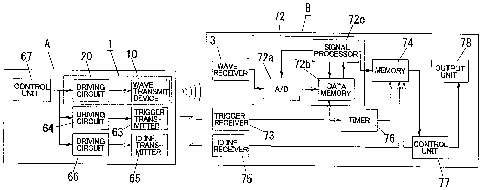
As shown in FIG. 11, the wave transmission comprises a unit
110 comprises a trigger signal transmitter 63 for transmitting a trigger
signal with using a light or a radio wave, a driving circuit 64 for
driving the trigger signal transmitter 63, an identification information
signal transmitter 65 for transmitting an inherent identification
information signal with using light, radio wave or acoustic wave, a
driving circuit 66 for driving the identification information signal
transmitter 65, and a control unit 67 for controlling the driving
CA 02574028 2007-01-16
WO 2006/011650 PCT/JP2005/014164
39
circuits 20, 64 and 66, further to the above-mentioned wave
transmitting device 10 and the driving circuit 20 for driving the wave
transmitting device 10.
Timing for starting transmission of an acoustic wave from the
wave transmitter 1, timing for starting transmission of a trigger signal
from the trigger signal transmitter 63, and timing for transmitting an
identification information signal from the identification information
signal transmitter 65 are controlled by the control unit 67. The
control unit 67 is mainly comprised of a microcomputer, and the
above each function of the control unit 67 is realized by executing an
appropriate program in the microcomputer.
The wave receiving unit 120 comprises the wave receiver 3, a
trigger signal receiver 73 for outputting a trigger receiving signal
when it receives the trigger signal transmitted from the trigger signal
transmitter 63, an identification signal receiver 75 for identification
information signal transmitter 65, a position calculator 72 for
calculating and outputting a relative position of the wave transmitter
1 with respect to the wave receiver 3 (an orientation where the wave
transmitter 1 is located and a distance to the wave transmitter 1) on
the basis of wave receiving signals outputted from the wave receiver
3 and the trigger receiving signal outputted from the trigger signal
receiver 73, a timer 76 for outputting a time when it receives the
trigger receiving signal from the trigger signal receiver 73
(hereinafter abbreviated as trigger receiving time), and a memory 74
for memorizing result of calculation (the orientation where the wave
CA 02574028 2007-01-16
WO 2006/011650 PCT/JP2005/014164
transmitter 1 is located and the distance to the wave transmitter 1)
outputted from the position calculator 72 in time-series homologizing
with the trigger receiving time outputted from the timer 76.
The trigger receiving time memorized in the memory 74, the
orientation where the wave transmitter 1 is located and a distance to
the wave transmitter 1 at each trigger receiving time (that is, data
relating to variation of relative position on the wave transmitter 1
mounted on each migration object 4 in time-series) are converted to
data array of data transmission form of an output unit 78 by a control
unit 77 so as to be outputted to an administration apparatus such as an
external computer through the output unit 78. As for the output unit
78, for example, a serial transmission interface such as
TIA/EIA-232-E or USB, or a parallel transmission interface such as
SCSI can be used. The above function of the control unit 77 is
realized by executing an appropriate program in the microcomputer.
When light is used as the trigger signal, for example, a light
emitting diode is used for the trigger signal transmitter 63.
Alternatively, when radio wave is used as the trigger signal, for
example, a radio wave transmitter is used for the trigger signal
transmitter 63. Since light and radio wave are much faster than
acoustic wave, a term for arriving light or radio wave can be regarded
as zero in a time region while an acoustic wave reaches from the wave
transmitting unit 110 to the wave receiving unit 120.
When light is used as the identification information signal, for
example, a light emitting diode is used for the identification
CA 02574028 2007-01-16
WO 2006/011650 PCT/JP2005/014164
41
information signal transmitter 65. Alternatively, when radio wave is
used as the identification information signal, for example, a radio
wave transmitter is used for the identification information signal
transmitter 65. Furthermore, when acoustic wave is used as the
identification information signal, for example, the thermally induced
acoustic wave generator is used for the identification information
signal transmitter 65.
As shown in FIG. 10B, the wave receiver 3 of the wave
receiving unit 120 has a plurality of wave receiving devices 30 (in the
figure, four devices are illustrated as an example) each for receiving
an acoustic wave transmitted from the wave transmitting device 10
and for transmitting the received acoustic wave to a wave receiving
signal of an electric signal. Each wave receiving device 30 is
two-dimensionally arranged on the same substrate 39. A distance L
(a pitch of arrangement) between the centers of the wave receiving
devices 30 is desirable to be set to a wavelength extent of an acoustic
wave generated by the wave transmitting device 10 (for example, 0.5
to 5 times of the wavelength of the acoustic wave). If the distance L
between the centers of the wave receiving devices 30 is shorter than a
half of the wavelength of the acoustic wave, a time difference
between the times when the acoustic waves reach to adjoining two
wave receiving devices 30 becomes too short to detect the time
difference. As for the wave receiving devices 30, for example, the
above electric .capacitance microphones as described in the first
embodiment can be used. Since the electric capacitance microphone
CA 02574028 2007-01-16
WO 2006/011650 PCT/JP2005/014164
42
has a Q factor much smaller than that of the piezoelectric device, it is
possible to make a region of frequency of receivable acoustic waves.
When light is used as the trigger signal transmitted from the
trigger signal transmitter 63, for example, a photo-diode is used for
the trigger signal receiver 73. Alternatively, when radio wave is
used as the trigger signal, for example, a radio wave receiving
antenna is used for the trigger signal receiver 73. As for the trigger
signal receiver 73, an apparatus, which can receive the trigger signal,
convert the trigger signal to an electric signal (trigger receiving
signal) and output the electric signal, can be used.
When light is used as the identification information signal
transmitted from the identification information signal transmitter 65,
for example, a photo-diode is used for the identification information
signal receiver 75. Alternatively, when radio wave is used as the
identification information signal, for example, a radio wave receiving
antenna is used for the identification information signal receiver 75.
Furthermore, when acoustic wave is used as the identification
information signal, for example, an electric capacitance microphone is
used for the identification information signal receiver 75. As for the
identification information signal receiver 75, an apparatus, which can
receive the identification information signal, convert the
identification information signal to identification information of
electric signal and output the electric signal, can be used.
The position calculator 72 has a function for demanding an
azimuth angle 0 where the wave transmitter 1 is located with respect
CA 02574028 2007-01-16
WO 2006/011650 PCT/JP2005/014164
43
to the wave receiver 3 (an orientation from which an acoustic wave
arrives) on the basis of the phase difference between the acoustic
waves received by the wave receiving devices 30 of the wave receiver
3 and the arrangement of the wave receiving devices 30.
Subsequently, the position calculator 72 is described. In'
order to simplify the description, the wave receiving devices 30 of the
wave receiver 3 is illustrated to be arranged one-dimensionally on the .
same plane as shown in FIG. 12. In addition, FIG. 12 is substantially
the same as FIG. 2 except a number of the wave receiving devices 30.
FIGs. 13A to 13C respectively show the wave receiving signals
of the wave receiving devices 30 shown in FIG. 12 when a driving
voltage having a waveform of a half period of a sinusoidal waveform
is applied to the heating conductor layer 13 of the thermally induced
acoustic wave generator constituting the wave transmitting device 10.
FIG. 13A shows the waveform of the wave receiving signal outputted
from the wave receiving device 30 disposed at uppermost position in
FIG. 12. FIG. 13B shows the waveform of the wave receiving signal
outputted from the wave receiving device 30 disposed at middle
position in FIG. 12. FIG. 13C shows the waveform of the wave
receiving signal outputted from the wave receiving device 30
disposed at undermost position in FIG. 12.
The position calculator 72 comprises a signal processor 72c
having a function for detecting an orientation where the wave
transmitter 1 is located with respect to the wave receiver 3 (an
orientation from which the acoustic wave arrives) on the basis of the
CA 02574028 2007-01-16
WO 2006/011650 PCT/JP2005/014164
44
phase difference of the acoustic waves received by the wave receiving
devices 30 of the wave receiver 3 and the arrangement of the wave
receiving devices 30.
The signal processor 72c comprises a delay function for
delaying the wave receiving signals which are electric signals
outputted from the wave receiving devices 30 of the wave receiver 3
in predetermined delay times corresponding to an arrangement pattern
of the wave receiving devices 30 and for outputting the delayed wave
receiving signals as a group, an adding function for adding each
group of the delayed wave receiving signals, and a judging function
for comparing a magnitude relation between a peak value of an output
waveform of the added and delayed wave receiving signals and a
predetermined threshold value and for judging an orientation
corresponding to a delay time which is set at a time when a peak
value exceeds to the threshold value appears as the orientation where
the wave transmitter 1 is located (the orientation from which the
acoustic wave arrives).
The position calculator 72 comprises an A/D converter 72a for
converting an analogue wave receiving signal outputted from each
wave receiving device 30 of the wave receiver 3 to a digital wave
receiving signal and outputting the converted digital wave receiving
signal, and a data memory 72b for memorizing outputs from the A/D
converter 72a in a predetermined wave receiving term from a time
when the trigger receiving signal from the trigger signal receiver 73 is
inputted, further to the signal processor 72c.
CA 02574028 2007-01-16
WO 2006/011650 PCT/JP2005/014164
The signal processor 72c sets a wave receiving term when the
trigger receiving signal is inputted to' the data memory 72b, and drives
the A/D converter 72a only while the wave receiving term for
obtaining an orientation where the wave transmitter 1 is located with
using the data of wave receiving signals stored in the data memory
72b while the wave receiving term. The signal processor 72c is
configured by a microcomputer and so on. In addition, [a number of
wave receiving devices 30] X [a number of data of signal receiving
signals from each wave receiving device] of data are stored in the
data memory 72b.
In the position detecting system of the fourth embodiment, a
thermally induced acoustic wave generator is used as the wave
transmitting device 10 of the wave transmitter 1. Therefore, it is
assumed that the acoustic waves arrive at the wave receiver 3 from
two orientations as shown in FIG. 14, and the acoustic waves from the
orientation having an azimuth angle 01 arrives earlier than the
acoustic waves from the orientation having the azimuth angle 02. As
shown in FIGs. 15A to 15C, two groups of wave receiving signals
rarely overlap each other. As a result, the azimuth angles 01 and 02
where the wave transmitters 1 mounted on the migration objects 4 are
located (orientation from which the acoustic waves arrive) can be
obtained.
FIG. 15A shows waveforms of two wave receiving signals of
the wave receiving device 30A at uppermost position in FIG. 14.
FIG. 15B shows waveforms of two wave receiving signals of the wave
CA 02574028 2007-01-16
WO 2006/011650 PCT/JP2005/014164
46
receiving device 30B at middle position in FIG. 14. FIG. 15C shows
waveforms of two wave receiving signals of the wave receiving
device 30C at undermost position in FIG. 14. The waveform
disposed at left hand in each of FIGs. 15A to 15C corresponds to the
acoustic wave arriving from the orientation having the azimuth angle
01, and the waveform disposed at right hand corresponds to the
acoustic wave arriving from the orientation having the azimuth angle
02.
When a distance (delay distance) between a wave front of the
acoustic wave which will arrive at a wave receiving device 30B and a
center of adjoining another wave receiving device 30C when the
acoustic wave arrives at the wave receiving device 30C is designated
by a symbol "dl" (see FIG. 14), a time difference Atl necessary for
arriving the wave front of the acoustic wave at the wave receiving
device 30B (see FIGs. 15A to 15C) is calculated by the equation
At l =d l /c=L = sin 01 /c. On the other hand, when a distance (delay
distance) between a wave front of the acoustic wave which will arrive
at a wave receiving device 30B and a center of adjoining another
wave receiving device 30A when the acoustic wave arrives at the
wave receiving device 30A is designated by a symbol "d2" (see FIG.
14), a time difference At2 necessary for arriving the wave front of the
acoustic wave at the wave receiving device 30B (see FIGs. 15A to
15C) is calculated by the equation At2=d2/c=L-sin 02/c.
The signal processor 72c of the position calculator 72
comprises a distance calculating function for calculating a distance
CA 02574028 2007-01-16
WO 2006/011650 PCT/JP2005/014164
47
from the wave receiver 3 to the wave transmitter 1 from a relation
between a time when the trigger signal is received by the trigger
signal receiver 73 and a time when the acoustic waves are received by
the wave receiving devices 30. Since a signal such as light or radio
wave which is much faster than acoustic wave is used as the trigger
signal, a term necessary for transmitting the trigger signal from the
wave transmitting unit 110 to the wave receiving unit 120 is
vanishingly shorter. The signal processor 72 calculates the distance
between the wave receiver 3 and the wave transmitter 1 with using a
time difference T from a time when the trigger signal ST is received
to a time when the wave receiving signal SP is received first after
receiving the trigger signal ST as shown in FIGs. 16A to 16C and
acoustic velocity. The distance calculating function of the signal
processor 72c can be realized by executing an appropriate program
with a microcomputer constituting the signal processor 72c.
In the above-mentioned position detecting system of the fourth
embodiment, orientations where the wave transmitters 1 mounted on
the migration objects 4 in a detectable area around a wave receiver 3
of a wave receiving unit 120 installed on a ceiling 200 can be
detected. In comparison with the conventional position detecting
system in which a plurality of acoustic wave receivers (wave
receivers) are installed on the ceiling with predetermined distances,
the application of the position detecting system becomes easier, and
the arrangement of the wave receivers 3 becomes easier.
In the acoustic wave sensor in the position detecting system of
CA 02574028 2007-01-16
WO 2006/011650 PCT/JP2005/014164
48
the fourth embodiment, an acoustic wave generating device, which
generates an acoustic wave by applying thermal impact to the air, and
has a Q factor of resonance characteristic much smaller than that of a
piezoelectric device, is used as the wave transmitting device 10, and
electric capacitance microphones each having a Q factor of resonance
characteristic much smaller than that of the piezoelectric device are
used as the wave receiving devices 30. Thus, in comparison with the
case of using the piezoelectric devices as both of the wave
transmitting device and the wave receiving devices, it is possible not
only to shorten a dead zone caused by reverberation component
included in an acoustic wave transmitted from the wave transmitting
device 10 and a dead zone caused by reverberation component
included in wave receiving signals outputted from the wave receiving
devices 30, but also to increase angular resolution of the acoustic
wave sensor.
When a floor 100 is flat and a height from the floor 100 to a
ceiling 200 is constant in a building to which the position detecting
system of the fourth embodiment is applied, and a size of migration
objects 4 are constant (that is a height from the floor 100 to an upper
face of the migration objects 4 are constant), a distance between a
plane including a wave receiver 3 and parallel to the ceiling 200 and a
plane including a wave transmitter 1 and parallel to the ceiling 200
becomes constant with no relation to a position of the migration
object 4 on the floor 100. Thus, when such a constant distance is
previously memorized into a memory of a microcomputer as known
CA 02574028 2007-01-16
WO 2006/011650 PCT/JP2005/014164
49
distance information (height information), it is possible to obtain a
distance between the wave receiver 3 and the wave transmitter 1 from
the distance information and an orientation where the wave
transmitter 1 is located.
On the other hand, even when a step 100b exists on the floor
100, it is possible to obtain a distance between the wave receiver 3 of
the wave receiving unit 120 and the wave transmitter 1 of the wave
transmitting unit 110 precisely by the signal processor 72c on the
basis of a relation between a time when the trigger signal is received
by the trigger signal receiver 73 and a time when acoustic waves are
received by the wave receiving devices 30.
The control unit 77 has a sound source identifying function for
identifying. the wave transmitter 1 mounted on each migration object
4 individually on the basis of the identifying information outputted
from the identification information signal receiver 75 and memorized
in the memory 74. Thus, even when a plurality of migration objects
4 is located in a detectable area in which the wave receiver 3 can
receive acoustic waves, relative positions of the wave transmitters 1
with respect to the wave receiver 3, that is the relative positions of the
migration objects 4 can be obtained.
For example, when four migration objects 4 are located, it is
possible to use identification information signals respectively
comprised of different pulse arrays, as shown in FIGs. 18A to 18D
can be used as the identification information signals transmitted from
the identification information signal transmitters 65 of the wave
CA 02574028 2007-01-16
WO 2006/011650 PCT/JP2005/014164
transmitting units 110 of the migration objects 4. In such a case, the
results of calculation by the signal processor 72c of the position
calculator 72 are memorized in the memory 74 in compliance with the
identification information. In the control unit 77, an orientation
where a wave transmitter 1 is located (an orientation from which
acoustic waves arrive) and a distance between the wave receiver 3 and
the wave transmitter 1 obtained by the position calculator 72 can be
distinguished from which wave transmitting units 110.
Furthermore, when it is assumed that light or radio wave is
used as the identification information signal, and only one wave
transmitting unit 110 is located in a detectable area of the wave
receiver 3 in which the wave receiver 3 can receive the acoustic
waves, relations between the identification information outputted
from the identification information signal receiver 75 and the wave
receiving signals outputted from the wave receiving devices 30 of the
wave receiving unit 120 are shown in FIGs. 19A to 19C. FIG. 19A
shows a waveform of the wave receiving signal of the wave receiving
device 30 at uppermost position in FIG. 12. FIG. 19B shows a
waveform of the wave receiving signal of the wave receiving device
30 at middle position in FIG. 12. FIG. 19C shows a waveform of the
wave receiving signal of the wave receiving device 30 at undermost
position in FIG. 12. In this case, the identification information
signal transmitter 65 can serve as the above trigger signal transmitter
63, and the identification information signal SI can be used as a
trigger signal. Furthermore, it is possible to provide the above
CA 02574028 2007-01-16
WO 2006/011650 PCT/JP2005/014164
51
sound source identifying function into the position calculator 72.
In the position detecting system of the fourth embodiment, the
trigger signal transmitter 63 is provided on the wave transmitting unit
110 and the trigger signal receiver 73 is provided on the wave
receiving unit 120, but the configuration of the position detecting
system is not limited to this. Contrary to the above-mentioned
description, it is possible to provide the trigger signal transmitter 63
on wave receiving unit 120, and the trigger signal receiver 73 is
provided on the wave transmitting unit 110. In such a case, the
control unit 67 of the wave transmitting unit 110 controls the driving
circuit 20 so that an acoustic wave is transmitted from the wave
transmitting device 10 on the basis of the output from the trigger
signal receiver 73, and the signal processor 72c of the position
calculator 72.obtains a distance to the wave transmitter 1 from
relations between a time when a trigger signal is transmitted from the
trigger signal transmitter 63 and times when acoustic waves are
received by the wave receiving devices 30. Furthermore, it is
possible to constitute the control unit 67 of the wave transmitting unit
110 so that it drives the driving circuit 20 just after receiving the
trigger receiving signal outputted from the trigger signal receiver 73
or after passing a predetermined term from receiving the trigger
receiving signal.
In addition, in the above position detecting system, the wave
transmitter 1 is mounted on the migration object 4 and the wave
receiver 3 is installed on a settlement face such as the ceiling 200. It,
CA 02574028 2007-01-16
WO 2006/011650 PCT/JP2005/014164
52
however, is possible to provide the wave transmitter 1 on a settlement
face and the wave receiver 3 is mounted on the migration object 4.
This application is based on Japanese patent applications
2004-219330, 2004-219331, 2005-5639, 2005-5640 and 2005-86787
filed in Japan, the contents of which are hereby incorporated by
references.
Although the present invention has been fully described by
way of example with reference to the accompanying drawings, it is to
be understood that various changes and modifications will be apparent
to those skilled in the art. Therefore, unless otherwise such changes
and modifications depart from the scope of the present invention, they
should be construed as being included therein.