Note: Descriptions are shown in the official language in which they were submitted.
CA 02576590 2007-01-30
TEST CIRCUIT BOARD AND METHOD FOR TESTING A TECHNOLOGY USED TO
MANUFACTURE CIRCUIT BOARD ASSEMBLIES
Field of the invention
The present invention relates to the field of reliability control of circuit
board
assembly manufacturing technologies and more particularly to test circuit
board, test
circuit board assemblies and method using the same for testing such
technologies.
Technical background
Until recently, most of the electrical and electronic products commercialized
in
the marketplace, such as consumer electronics devices like cell phones and
computers,
have been manufactured with circuit board assembling processes using lead-
containing
alloys to perform soldering, such as the well-known eutectic tin-lead (Sn-Pb)
alloy. The
always growing worldwide market for these electronic/computer- based products
combined with still shorter lifecycle characterizing such products have
resulted in a
significant increase of obsolete products waste (E-waste), the disposal of
which having
detrimental effects to the environment. To address that problem, governmental
authorities have issued specific directives aimed at restricting the use of
hazardous
siubstances found in electrical and electronic products to promote recycling
and limit the
quantity of waste going to disposal in the environment. For example, the
European
commission has issued a directive entitled: "Restriction of the Use of certain
Hazardous
Substances in Electrical and Electronic Equipment (RoHS)" which contains
incentives
for the product suppliers to design and manufacture electrical and electronic
equipment
in a more environmental-friendly way, considering waste management issues.
European commission has also issued a directive entitled: "Waste Electrical
and
Electronic Equipment (WEEE)" /95/EC t requiring the substitution of numerous
heavy
metals such as lead, mercury and cadmium used in the manufacturing of printed
circuit
boards (PCB's) by less hazardous or non-toxic substances. As a consequence of
the
application of such new environmental rules, the designers and manufacturers
of
electrical and electronic products are required to change or adapt their
product
manufacturing processes accordingly. The implementation of new circuit board
production processes requires the manufacturers to evaluate process
reliability
especially regarding the substitution of circuit board surface finish
compounds and
soldering alloys usually used assemble electrical and electronic components
onto the
circuit boards.
CA 02576590 2007-01-30
2
Highly Accelerated Life Testing (HALT), Environmental Stress Screening (ESS)
and Highly Accelerated Stress Screening (HASS) are product reliability test
standards
generally accepted by the electronic industry to allow the identification and
assessment
of faults related to PCB design and manufacturing technologies. These testing
standards can be used to control the manufacturing quality of electrical and
electronic
products produced with new lead-free manufacturing processes. The testing is
performed using environmental stimulus such as vibration, thermal variation,
shock or
humidity, combined with functional measurements made while subjecting the
product to
these environmental stimulus. To provide qualification testing in the context
of
electronic product development, it is known to use a test circuit board
assembly for
evaluating the quality of a circuit board mounting technology, as the
evaluation board
disclosed in U.S. Patent 6,888,360 B1 issued to Connell et al., which board is
provided
with a plurality of board pad matrix patterns formed on the board substrate
surface,
where the pad-to-pad spacing, pad shape and pad size can be chosen to
correspond to
the particular characteristics of the component packaging used, such as Quad
Flat
Package (QFP), Small Outline Package (SOP), Ball Grid Array (BGA), Chip Scale
Package (CSP) and the like, so as that the component terminals of each
electronic
component is properly aligned with the corresponding board pads covered with
solder
paste disposed on the circuit board substrate surface. The evaluation board as
taught
by Connell et al. is designed such that sizes of the board pads in the
patterns and the
pad-to-pad spacing of the board pads are varied over the substrate surface
allowing all
characteristics of a surface-mount technology to be tested under uniform
conditions.
Such evaluation board is used to conduct quality assessment tests such as open-
pad
detection characterized by an absence of solder paste, or shorted pads
(bridging) that
can occur during various stage of a SMT process, which tests being made by
visual
observation through manual means or automated visual inspection means. Another
circuit board manufacturing technology qualification testing approach of the
prior art for
use in product development is disclosed in U.S. Patent 6,806,718 B2 issued to
Berkley,
which makes use of a test assembly containing a surrogate circuit board and
surrogate
electronic components mounted thereon, wherein terminals of components are
joined
by wiring to respective bounding pads on the circuit board to form bounded
joints in a
configuration producing one or more test series circuits. A tester supported
on the
circuit board monitors each test series circuit to produce a persistent
indication when a
break occurs in a bounded joint or portion of the test series circuit when
subjecting the
test assembly to stresses such as temperature variation, vibration or shock. A
similar
approach for analyzing soldered joint fractures in response to external
stimulus is
CA 02576590 2007-01-30
3
disclosed in U.S. Patent 6,564,986 B1 issued to Hsieh, wherein a test assembly
uses a
particular integrated circuit (IC) package including solder balls
interconnected in pairs
with conductors to form a first daisy chain portion and a PCB provided with
pairs of
contact pads and test pads interconnected by conductive structures to form a
second
daisy chain portion, in such a manner than when the IC package is mounted on
the
PCB by a soldering process, pairs of connected soldered balls and associated
pairs of
connected contact pads form a complete daisy chained conductive path through
all
soldered balls between first and second test pads. In practice, such test
circuit board
assembly might not provide the flexibility required by still shorter
electronic product
design lifecycles or by the need for fast transition from existing
manufacturing process
to new process complying with new evolving environmental regulations.
Summary of invention
According to the present invention, from a broad aspect, there is provided a
test
circuit board for use with components each having connecting terminals and
being
characterized by one of a plurality of predetermined packaging types, and with
an
electrical continuity tester. The test circuit board comprises a substrate
having at least
one surface adapted to mount selected one or more of said components thereon,
at
least one circuit carried by the substrate, comprising a set of component
connection
sites interconnected by conducting traces and including, for each
predetermined
packaging type, at least one connection site having at least one input contact
pad and
at least one output contact pad adapted to be electrically bond to
corresponding
connecting terminals of the component characterized by the packaging type. The
circuit
further comprises a set of pairs of connecting areas associated with the set
of
component connection sites, the areas of each pair being in electrical
communication
respectively with the input contact pad and the output contact pad of the
component
connection site to which it is associated. The test circuit board further
comprises board
leads carried by the substrate and adapted to interface the circuit with the
electrical
continuity tester, wherein the connecting areas of any one of said pairs not
associated
with the component connection sites adapted to connect the selected components
are
capable of being shorted to enable the use of the test circuit board with the
electrical
continuity tester.
According to the present invention, from a further broad aspect, there is
provided a test circuit board assembly for use with an electrical continuity
tester,
comprising a substrate having at least one component mounting surface, at
least one
circuit carried by the substrate, comprising a set of component connection
sites
interconnected by conducting traces and including, for each one of a plurality
of
CA 02576590 2007-01-30
4
component packaging types, at least one connection site having at least one
input
contact pad and at least one output contact pad adapted to be electrically
bonded to
corresponding connecting terminals of a component characterized by the
packaging
type. The circuit further comprises a set of pairs of connecting areas
associated with
said set of component connection sites, the areas of each pair being in
electrical
communication respectively with the input contact pad and the output contact
pad of the
component connection site to which it is associated, one or more selected
components
each being characterized by one of said plurality of predetermined packaging
types and
each having connecting terminals being bonded to the contact pads provided on
one of
said connection sites corresponding to the packaging type characterizing the
selected
component, and board leads carried by said substrate and adapted to interface
said
circuit with the electrical continuity tester, wherein the connecting areas of
any one of
said pairs not associated with the component connection sites connecting said
selected
components are capable of being shorted to enable the use of the test circuit
board
assembly with the electrical continuity tester.
According to the present invention, from another broad aspect, there is
provided
a test circuit board assembly for use with an electrical continuity tester,
comprising a
substrate having at least one component mounting surface, at least one circuit
carried
by the substrate, comprising a set of component connection sites
interconnected by
conducting traces and including, for each one of a plurality of component
packaging
types, at least one connection site having at least one input contact pad and
at least
one output contact pad adapted to be electrically bonded to corresponding
connecting
terminals of a component characterized by said packaging type. The circuit
further
comprises a set of pairs of connecting areas associated with said set of
component
connection sites, the areas of each pair being in electrical communication
respectively
with the input contact pad and the output contact pad of the component
connection site
to which it is associated. The test circuit board assembly further comprises
one or
more selected components each being characterized by one of said plurality of
predetermined packaging types and each having connecting terminals being
bonded to
the contact pads provided on one of said connection sites corresponding to the
packaging type characterizing the selected component, board leads carried by
the
substrate and adapted to interface said circuit with said electrical
continuity tester; and
means for selectively shorting the connecting areas of any one of said pairs
not
associated with the component connection sites connecting said selected
components,
to enable the use of the test circuit board assembly with the electrical
continuity tester.
CA 02576590 2007-01-30
According to the present invention, from a further broad aspect, there is
provided a method for testing a technology used to manufacture circuit board
assemblies, comprising the steps of: i) providing a test circuit board
comprising: a
substrate having at least one component mounting surface; at least one circuit
carried
5 by the substrate, comprising a set of component connection sites
interconnected by
conducting traces and including, for each one of a plurality of component
packaging
types, at least one connection site having at least one input contact pad and
at least
one output contact pad adapted to be electrically bonded to corresponding
connecting
terminals of a component characterized by said packaging type, the circuit
further
comprising a set of pairs of connecting areas associated with said set of
component
connection sites, the areas of each said pair being in electrical
communication
respectively with the input contact pad and the output contact pad of the
component
connection site to which it is associated; board leads carried by said
substrate and
being in electrical communication with test locations on said circuit; ii)
providing one or
more selected components to be mounted on the component mounting surface, each
being characterized by one of said plurality of predetermined packaging types
and each
having connecting terminals; iii) using said technology to bond the connecting
terminals
of the selected component to the contact pads provided on one of said
connection sites
corresponding to the packaging type characterizing the selected component, to
produce
a test circuit board assembly; iv) shorting the connecting areas of any one of
said pairs
not associated with the component connection sites connecting said selected
components; and v)checking the electrical continuity of the circuit between
the board
leads.
According to the present invention, from a still further broad aspect, there
is
provided a method for testing a technology used to manufacture circuit board
assemblies, comprising the steps of: i) providing a test circuit board
assembly
comprising: a substrate having at least one component mounting surface; at
least one
circuit carried by the substrate, comprising a set of component connection
sites
interconnected by conducting traces and including, for each one of a plurality
of
component packaging types, at least one connection site having at least one
input
contact pad and at least one output contact pad adapted to be electrically
bonded to
corresponding connecting terminals of a component characterized by said
packaging
type, the circuit further comprising a set of pairs of connecting areas
associated with
said set of component connection sites, the areas of each said pair being in
electrical
communication respectively with the input contact pad and the output contact
pad of the
component connection site to which it is associated; one or more selected
components
CA 02576590 2007-01-30
6
each being characterized by one of said plurality of predetermined packaging
types and
each having connecting terminals being bonded using said technology to the
contact
pads provided on one of said connection sites corresponding to the packaging
type
characterizing the selected component; and board leads carried by the
substrate and
being in electrical communication with test locations on said circuit; ii)
shorting the
connecting areas of any one of said pairs not associated with the component
connection sites connecting said selected components; and iii) checking the
electrical
continuity of the circuit between the board leads.
Brief description of the drawings
Preferred embodiments of the test circuit board, test circuit board assembly
and
method for testing a technology used to manufacture test circuit board
assemblies, will
now be described in detail in view of the accompanying drawings in which:
Figs. 1 a and lb are schematic plan views of top and bottom (mirror view)
surfaces of a test circuit board, respectively, showing the location of areas
adapted to
receive electrical and electronic components to be mounted on the board;
Fig. 2 presents respective block diagrams of four distinct circuits having
component connection sites designed to implement daisy-chains of integrated
circuits
disposed on corresponding locations on the circuit board top and bottom
surfaces
shown in Figs. 1a and 1b, so as to form a test board circuit assembly;
Fig. 3 presents respective block diagrams of two circuits having component
connection sited adapted to receive resistor chains at respective locations of
top and
bottom board surfaces of Figs. 1a and 1b as part as the test circuit board
assembly;
Fig. 4 presents respective block diagrams of two circuits having component
connection sited adapted to receive chains of resistor networks at respective
locations
of top and bottom board surface of Figs. 1 a and lb as part of the test
circuit board
assembly;
Fig. 5 presents respective block diagrams of two capacitor chains to be
mounted on respective top and bottom board surfaces of Figs. 1a and 1b as part
as the
test circuit board assembly;
Fig. 6 (parts I-II) is a plan view of top surface of the test circuit board of
Fig. 1a,
showing the actual location thereon of the component connection sites
according to a
12-layer implementation example;
Fig. 7 (parts I-II) is a plan view of bottom surface of the test circuit board
of Fig.
1a, showing the actual location thereon of the component connection sites
according to
the implementation example;
CA 02576590 2007-01-30
7
Fig. 8 is a plan view of a first, top layer as part of the circuit board of
Fig. 1a,
showing the layout of component sites and conducting traces forming some of
the
circuits incorporated in the test circuit board according to the
implementation example;
Fig. 9 is a plan view of a second circuit board layer disposed directly under
the
top layer of Fig. 8, showing the internal conductor pattern of the Bald Grid
Array
connection sites and main vias extending through the board substrate according
to the
implementation example;
Fig. 10 is a plan view of the layout used by nine superimposed identical
circuit
layers disposed under second layer of Fig. 9, showing vias pattern associated
with Ball
Grid Arrays receiving sites and main vias further extending through the
circuit substrate
according to the implementation example;
Fig. 11 is a plan view of a last, bottom layer as part of the circuit board of
Fig.
1 b, showing the layout of component sites and conducting traces forming some
other
circuits incorporated in the test circuit board according to the
implementation example;
Fig. 12 is a photographic view of the top surface of an actual test circuit
board
assembly according to the design of Fig. 6, showing some components mounted
thereon;
Fig. 13 is a photographic view of the bottom surface of the actual test
circuit
board according to the design of Fig. 7, showing some other components mounted
thereon;
Fig. 14 is a graph presenting temperature curves in function of time
characterizing a heating-cooling stimulus cycle that was applied while testing
a test
circuit board assembly;
Fig. 15 is a graph representing acceleration profile curves as a function of
vibration frequency characterizing a vibratory stimulus that was applied to a
test circuit
board assembly;
Figs. 16A and 16B are graphs presenting resistance (impedance) data in
function of scan number as a result of testing a circuit board assembly while
applying
vibration effective levels of 5g and 10g, respectively;
Figs. 17 is a graph presenting resistance (impedance) data in function of scan
number as a result of testing another circuit board assembly while applying
vibration
effective levels of 20g.
Detailed description of the preferred embodiments
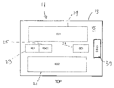
Referring to Fig. 1a, there is shown a test circuit board generally designated
at
11 including a substrate having a top surface 15 that is adapted to mount
selected one
or more electrical and/or electronic components thereon, such as integrated
circuits
CA 02576590 2007-01-30
8
(IC's), resistors, capacitors, inductors, rectifiers and/or transistors
available in various
packages. Although circuit board 13 can be provided with only its top surface
being
populated with components, its bottom surface as designated at 17 on Fig. 1 b
can also
be adapted to mount further selected one or more components thereon. It is
pointed out
that Fig. lb is a schematic mirror view of the bottom surface of circuit
substrate 13 to
better show the actual alignment of respective circuits provided on both top
and bottom
surfaces 15 and 17. Turning back to Fig. 1a, the board substrate shown carries
first
and second circuits 19, 21 adapted to form first and second integrated
circuits chains
(ICC1, ICC2), a third circuit 23 adapted to form a first resistor chain (RC1),
a fourth
circuit 25 adapted to form a first resistor network chain (RNC1) and a fifth
circuit 27
adapted to receive a first capacitor chain (CC1). Similarly, as shown in Fig.
1 b, the
substrate 13 can also carry further circuits adapted to receive components to
be
mounted onto its bottom surface 17, which circuits, in the present example,
includes
sixth and seventh circuits 29, 31 adapted to form third and fourth integrated
circuits
chains (ICC3, ICC4), a eighth circuit 33 adapted to form second resistor chain
(RC2), a
ninth circuit 35 adapted to form a second resistor network chain (RNC2) and a
tenth
circuit 37 adapted to receive a second capacitor chain (CC2). It is pointed
out that the
ten circuits 19 to 37 are schematically represented in dotted lines in Figs. 1
a and lb to
indicate that portions of any such circuits may be located within one of a
plurality of
board layers depending on the complexity and number of components to be
connected
within these circuits. Turning back to Fig. 1a, the test circuit board 11 is
further
provided with leads carried by substrate 13 and adapted to interface circuits
19-37 with
an electrical continuity tester (not shown) through a connector 39 of a
standard type
(DB-25) in the example shown, the function of which leads and tester being
explained
below in detail.
Referring now to Fig. 2, circuits 19, 21, 29 and 31 are shown as comprising a
set of component connection sites schematically depicted in dotted lines by
blocks 41,
42, 43 and 44, respectively. The component sites 41, 42, 43 and 44 of each set
are
interconnected by conducting traces 46. Each circuit 19, 21, 29, 31 includes,
for each
one of a plurality of predetermined components packaging types, at least one
connection site having at least one input contact pad 48 and at least one
output contact
pad 50 adapted to be electrically bounded to corresponding connecting
terminals of the
component characterized by its packaging type. Associated with each set of
component
connection sites 41, 42, 43, 44, each one of circuits 19, 21, 29, 31 further
comprises a
set of pairs of connecting areas 52, 52' in electrical communication
respectively with
input contact pad 48 and output contact pad 50 of the component connection
site to
CA 02576590 2007-01-30
9
which it is associated through bypass conducting traces 54 and 54', for each
component connection site 41, 42, 43, 44 provided on each circuit 19, 21, 29
and 31,
respectively. It can be seen from Fig. 2 that each component connection site
41, 42, 43,
44 is adapted to receive a selected one of predetermined packaging types such
as
Small Outline Packages (SOP), Ball Grid Arrays (BGA), Chip Scale Packages
(CSP),
Thin Small Outline Packages (TSOP), Thin Shrink Small Outline Packages
(TSSOP),
Small Outline J-lead packages (SOLJ), Quad Flat Packages (QFP), Thin Quad Flat
Packages (TQFP) or Discrete Packages (DPAK). It is to be understood that any
other
type of available or custom integrated circuit packaging may be used with the
proposed
test circuit board 11 having a component site designed to receive such
packaging. A
brief description of some of such integrated circuits packages available in
the market
place is given in Table 1.
Daisy
Item Supplier Description Chain Notes
1 TopLine D2PAKE7A-TIN-DC123 Yes SnlOO
2 TopLine TSSOP16M25-DE-TIN Yes Sn100
3 TopLine SOLJ20/26M-TIN-DE Yes Sn100
4 TopLine TSOP32T19.7-T1-DE-TIN Yes Sn100
5 TopLine TQFP44T30-DE-TIN 1mm thick Yes SnlOO
6 TopLine BGA46T.75C-DC24 Yes SnAgCu
7 TopLine BGA256T1.27C-DC200 Yes SnAgCu
8 TopLine SBGA256T1.27C-DC200 Yes SnA Cu
9 TopLine QFN28M.8-TIN-DE Yes Sn100
10 Topline BGA256T1.27-DC200 Yes SnPb
11 Topline BGA46T.75-DC24 Yes SnPb
12 Digikey MCR01 MZPF10R0 resistor 10R 1% 0402 ROHS) No ROHS
13 Di ike RC0603FR-0710RL resistor 10R 1% 0603 ROHS) No ROHS
14 Digikey RC0805FR-0710RL resistor 10R 1% 0805 ROHS) No ROHS
Digikey EXB-28V472JX(resistor array 0402x4 conc 4.7kR No ROHS
16 Di ike ECJ-2VB1 E104K ca acitor 0.1 uf/25V 0805 No ROHS
17 Di ike GRM1 55F51 E104ZA01 D ca acitor 0.1 uf/25V 0402) No ROHS
TABLE 1
15 It can be seen from the data of Table 1 that while some components are
adapted to be
soldered onto corresponding receiving site with environmentally approved
soldering
alloy (SnlOO, SnAgCu, ROHS), some components are adapted to be soldered with
conventional SnPb alloy, thus allowing to compare leadless mounting technology
with a
conventional soldering process. Conveniently, the selected integrated circuit
packages
are of a daisy chain integrating, dummy type to allow simple circuit
continuity testing.
The test circuit board 11 further comprises, for each circuit 19, 21, 29 and
31, a pair of
board leads 40, 40' carried by the substrate 13, which are in electrical
communication
CA 02576590 2007-01-30
respectively with end conducting traces 56, 56' used as test locations
provided on each
circuit 19, 21, 29 and 31, to interface thereof with an electrical continuity
tester through
connector 39 shown in Fig. 1a. Turning back to Fig. 2, according to the
proposed
circuit board, the connecting areas 52, 52' of anyone of the connecting area
pairs which
5 is not associated with the component connection sites used to connect a
selected
component, are capable of being shorted to enable the use of the test circuit
board with
an electrical continuity tester. For so doing, each circuit 19, 21, 29, 31 is
adapted to be
used in combination with shorting means in the form a conducting element
designated
at 58, capable of selectively shorting any pair of connecting areas 52, 52'
not
10 associated with the component connection site(s) connecting the selected
component(s), thereby establishing electrical communication between these
connecting
areas 52, 52' and pads 48, 50 that are associated with an unused component
site 41,
42, 43, or 44, to enable the use of the test circuit board assembly with an
electrical
continuity tester. It can be seen from Fig. 2 that circuits 19, 21, 29 and 31
in the
present example are adapted to receive identical integrated circuits of the
selected
package types, so as to provide a better coverage of the substrate for testing
purposes.
However, it should be understood that a single such circuit or a plurality of
circuits
including different combinations of circuit type packages could also be used.
Although a
plurality of jumpers (JP1-JP52) are used as shorting means in the present
example,
any other appropriate conducting element capable of shorting the pairs of
connecting
areas 52,52', can be used, such as a cable, wire, connector, switch, solder
link or
fusible trace (as disclosed in U.S. Patent 6,936,775).
Turning now to Fig. 3, fifth and sixth circuits 60, 62 are shown, which are
typical resistor chain circuits presenting a similar configuration as compared
with
circuits 19, 21, 29, 31 described above, but including in this case component
connection sites 60, 61 enabling circuits 60, 62 to form respective resistor
chains no. 1
and 2, each being adapted to receive a given number of connected resistors
represented by a single standard resistor symbol 62 in Fig.3 to simplify the
illustration.
Each circuit 60, 62 is also provided with conducting traces 46, input contact
pad 48,
output contact pad 50, connecting areas 52, 52', bypass conducting traces 54,
54', end
conducting traces 56, 56' as well as conducting elements 58, as above
described in
detail in view of the circuits of Fig. 2. In the example shown in Fig. 3, each
resistor
series 63 includes ten (10) resistors of a particular packaging type as
indicated, which
is different than the packaging type employed by the other resistor series in
the circuit
60, 62. It can be also seen that circuits 60 and 62 forming resistor chains
no. 1 and no.
2 are identical to provide a better substrate coverage for testing. However,
it should be
CA 02576590 2007-01-30
11
understood that other combinations of resistors and resistor packaging types
may be
implemented in circuit to form resistor chains, for example a given component
site may
be designed to receive a single resistor of a particular type while the other
component
sites within the same chain may be adapted to receive a plurality of resistor
characterized by different packaging types. Here again, the selected
component(s) can
be selectively implemented in the circuit at the desired location, while
unused
connection site may be bypassed using conducting elements 58 in a same manner
than
it can be done with the circuits shown in Fig. 2 as described above. The
substrate 13 of
test circuit board 11 integrating resistor chain circuits 60 and 62 also
carries additional
pairs of board leads 61, 61' as part of connector 39 shown in Fig. 1a to
interface these
circuits with an electrical continuity tester.
Turning now to Fig. 4, seventh and eight chain circuits are shown at 64 and 66
using a plurality of component connection sites 68, 69 each adapted to receive
a
resistor network package also represented here by a single standard resistor
symbol at
70 for simplicity of illustration. Although additional circuits 64 and 66 may
be adapted to
be used in combination with conducting elements to provide bypassing of any
individual
resistor network 70, the example of Fig. 4 is provided to illustrate the fact
that only
some of the circuits provided on a particular test board can have such
feature,
depending upon the requirement of the test designed for the particular product
and
process involved. Also provided on the board substrate 13 are additional board
leads
71, 71' to respectively interface circuits 64 and 66 to the electrical
continuity tester.
Referring now to Fig. 5, another example of additional ninth and tenth test
circuits is presented, wherein circuits generally designated at 72 and 74
include
respective pairs of component connection sites 76,76' and 77,77'. The ninth
circuit 72
shown is adapted to receive a parallel-connected group of eight (8) capacitors
respectively numbered C9-C16 as generally designated at 78, and C1-C8 as
generally
designated at 79, which are associated with component connection sites 76. The
tenth
circuit 74 shown is adapted to receive a further parallel-connected group of
eight (8)
capacitors numbered C17-C24 as generally designated at 80, and C25-C32 as
generally designated at 81, which are associated with component connection
sites 77.
To operatively couple these capacitive circuits to an electrical continuity
tester, a
ground lead 83 is provided on the board substrate, and further component
connection
sites 86, 88 are respectively connected between lead 82 and component site 76
and
between board lead 84 and component site 77 to receive coupling resistors R61,
R62
as designated at 90 and 92. If desired, a pair of connecting areas 94, 94'
with
corresponding bypass conducting traces 95, 95' may be provided in each
circuits 72, 74
CA 02576590 2007-01-30
12
for use with a conducting element 96 whenever the corresponding connection
site has
not be used to mount a component thereon. It should also be understood that
some
application could require to provide the test board with connection sites
specifically
adapted to receive other categories of electrical or electronic components
such as
inductors, rectifiers or transistor packages.
Turning now to Fig. 6, showing an actual layout of the circuits and associated
components provided on the top surface 15 of substrate 13 of the test circuit
board 11
as described above, particular locations of first and second circuits 19, 21
forming
integrated circuit chains no. 1 and 2 are shown respectively at upper and
lower portion
of the layout. As part of circuit 19, the pairs of connecting areas 52, 52'
associated with
each component connecting site 41 are shown, which connecting areas 52, 52'
can be
used in combination with corresponding conducting elements as indicated by
indicia
JP1-JP10 also appearing on Fig. 2 in relation with each conducting element 58.
It can
be seen from Fig. 6 that the layout of circuit 21 implementing integrated
circuit chain no.
2 uses a symmetrical configuration as compared with circuit 19. Within the
left central
portion of board substrate,13 third and fourth circuits 23 and 29 respectively
implementing resistor chains no. 1 and 2 are shown, while fifth circuit 27 and
interface
connector 39 are shown within the right central portion of board substrate 13.
In the
example shown, amongst circuits 23, 25 and 27, only circuit 23 is provided
with pairs of
connecting areas 52, 52' for use with conducting element identified as JP27-
JP32 also
appearing on Fig. 2.
Turning now to Fig. 7 illustrating the layout of bottom substrate surface 17
of the
test circuit board shown in Fig. 1 b, are shown, at the upper portion of board
substrate
13, the locations of the component connection sites 43 of sixth circuit 29
implementing
integrated circuit chain no.3, and, at the lower portion of board substrate
13, the
locations of the component connection sites 44 of seventh circuit 31
implementing IC
chain no. 4. Conveniently, in view of Fig. 6, the pairs of connecting areas
52, 52' as
part of circuit 29 and for use with conducting element identified as JP11-JP20
are
disposed between circuits 19 and 23 at a location 29', to be accessible from
top surface
15 of board substrate 13, rather than disposed on bottom surface off board
substrate 13
shown in Fig. 7, allowing access to the connecting areas of all circuits from
a same
board surface. Similarly, as shown in Fig. 6, the connecting areas 52, 52'
associated
with circuit 31 implementing IC chain no. 4 and for use with conducting
element
identified as JP33-JP42 are conveniently disposed between circuits 21 and 23
at a
location 29'. Turning back to Fig. 7, at the right central portion of board
substrate 13 are
located eighth circuit 33 implementing resistor chain no. 2 and ninth circuit
34
CA 02576590 2007-01-30
13
implementing resistor network chain no.2, while within left central portion of
board
substrate 13 is located tenth circuit 36 implementing capacitor chain no. 2.
Turning
again to Fig. 6, it can be seen that connecting areas 52, 52' as part of
circuit 33 to be
used with conducting element numbered JP21-JP26 are accessible from top board
surface 15 and disposed between circuit 23 and connection areas location at
33', as
indicated at 33'.
Referring now to Fig. 8 to Fig. 11, actual circuit board layers that can be
used to
manufacture a 12-layer test circuit board are shown. In Fig. 8 representing
the top layer,
there is shown the layout of component sites and conducting traces forming
circuits 19,
21, 23, 25 and 27 as described above. Some components implemented in these
circuits
can be seen on the photographic view of Fig 12, showing the top surface of an
actual
test circuit board assembly according to the design of Fig. 6. In Fig. 9
representing the
second circuit board layer disposed directly under the top layer of Fig. 8,
there is shown
the internal conductor pattern designated at 41' and 42' of the Bald Grid
Array
connection sites (U2, U3, Ull, U12) designated at 41' and 42', and some pairs
of
connecting areas in the form of rows of vias generally designated at 53
extending
through the board substrate. In Fig. 10, representing the layout used by nine
superimposed identical circuit layers disposed under the second layer of Fig.
9, there is
shown the vias pattern generally designated at 41 " and 42" of the same Bald
Grid
Array connection sites (U2, U3, U11, U12) as referred to above in view of Fig.
9, with
rows of vias 53 further extending through the board substrate. In Fig. 11,
representing
the last, bottom layer of the board, there is shown the layout of component
sites and
conducting traces forming circuits 29, 31, 33 , 35 and 37 as described above.
Some
components implemented in these circuits can be seen on the photographic view
of Fig
13, showing the bottom surface of an actual test circuit board assembly
according to
the design of Fig. 7.
Various methods for testing a technology used to manufacture test circuit
board
assemblies with the aid of the test circuit board as described above, will now
presented
in detail in view of an experimental example involving a set of 12-layer
printed circuit
assemblies. Table 2 contains general information and summarized results about
a
series of tests that were performed with these test circuit board assemblies
characterized by manufacturing parameters (surface finish and soldering alloy
used), in
terms of fault detection according to various testing conditions.
CA 02576590 2007-01-30
14
Manufacturing
Test board parameters Fault description
no. Post- Thermal
Finish Alloy assembling testing Vibratory testing
non circuit no.3: 8g;
1 Ag SAC305 U26 applicable circuits no. 2,3, 8: 20 g;
circuit no.3: 2g;
2 Ni-Au SAC305 U26 applnon icable circuit no.4: 10 g;
circuit no. 1: 12 g;
circuits no.7,9,10 previously open;
circuit no.3: 2g;
3 Ag SAC305 U35 appl~able circuit no.1: 12 g;
circuit no.4: 18 g;
circuits no. 1,2,3,4,7,9,10: 20 g;
4 Ag SAC305 U35 none circuit no.4: 5g;
circuit no.3: 5g;
U26, U35, circuits no. 3,4: 10 g;
Ni-Au SAC305 U25 none
circuits no. 2, 3 4: 15 g;
circuits no. 2,3,4,7,9: 20 g;
6 Ag SAC305 PCBB a I~able circuit no.8: 10g;
7 Ni-Au SAC305 U2 - JP2 none circuit no.3: 20g; non 8 Ni-Au SAC305 none
applicable
none
9 Ag SAC305 none none circuit no.9: 20g;
none
Ni-Au SAC305 none applicable
11 Ni-Au SAC305 none none none
12 Ni-Au SAC305 none none none
13 Ag NC100C U3, U25 none none
14 Ag NC100C U25 a I non cable circuit no.2: lOg
TABLE 2
All the tests performed involved the following procedure. First, a test
circuit board is
5 manufactured according to a predetermined design such as the one described
above,
using a specific board manufacturing technology to be tested and with which
the end
product is planed to be produced. The test circuit board is therefore
characterized by
the manufacturing parameters of the manufacturing process, especially
including the
particular surface finish applied, such as Ag or Ni-Au based compound
available in the
10 marketplace. Then, the selected components to be mounted on one or both of
board
substrate surfaces, each of which being characterized by one of the
predetermined
CA 02576590 2007-01-30
packaging types, are provided. Then, using the chosen manufacturing
technology,
characterized by employing a particular soldering alloy such as SAC305 or
NCIOOC
available in the marketplace, the connecting terminals of each selected
components are
bounded to the contact pads of the connection site corresponding to the
packaging type
5 characterizing the selected component, to produce the test circuit board
assembly.
Next, the connecting areas that are not associated with the component
connection sites
used for connecting the selected components are shorted with the particular
shorting
means used. Finally, the electrical continuity of each circuit between the
corresponding
board leads is checked, which leads are electrical communication with the test
locations
10 on each circuit provided on the test board. For so doing, using an
appropriate
connector, the test circuit board assembly can be conveniently interfaced with
a tester
capable of automatically checking the electrical continuity of each circuit
between the
corresponding board leads used. Electrical continuity checking can be
performed by
measuring electrical resistance (impedance) of the circuit between its
corresponding
15 board leads, for then comparing the measured electrical resistance
(impedance) with a
predetermined limit value. Although any ohmmeter or multimeter can be used, a
measurement/data acquisition system integrating a resistance (impedance)
measurement function is conveniently used, as will be later explained in more
detail.
Alternately, the electrical continuity checking can also be performed through
electrical
conductance (admittance) using an appropriate instrumentation. While
electrical
continuity checking can be performed in normal, unstressed condition as part
of a post-
assembling basic test, the electrical continuity checking can also be
performed while
subjecting the test circuit board assembly to an external stimulus over a
range of
intensities and durations. Typically, a standard procedure such as HALT, ESS
or HASS
involving predetermined thermal and vibratory conditions are used for planning
and
conducting the tests. Alternately or in addition to thermal and vibratory
conditions, other
external stimulus can be considered such as mechanical shock and humidity
level
variation, depending upon the expected field of use of the end product. It
should be
understood that the test circuit board in its bare-board (non populated) form
can be built
using manufacturing parameters characterizing the technology used by a first
supplier,
while the mounting of these selected components onto the test circuit board
can be
made using a particular bounding technology characterized by specific
manufacturing
parameters as used by another supplier, resulting in the final test circuit
board
assembly. The testing procedures can also be performed by a third supplier
specialized
in testing services. The test circuit board, resulting test circuit board
assembly and
testing method hereinabove described can be used for manufacturing technology
CA 02576590 2007-01-30
16
proofing as a whole, considering bare-board manufacturing as well as component
assembling stages.
According to a test planning that was established for the series of tests
involving
the fourteen test circuit board assemblies numbered 1-14 in Table 2, three (3)
successive testing steps were performed. First, a post-assembling testing
procedure
was conducted to control the quality of assembling. Second, thermal testing
was
performed on selected test circuit board assemblies involving fast temperature
variations within a-40 C to +110 C range. Finally, vibratory testing was
conducted on
all fourteen (14) test circuit board assemblies. It should be understood that
vibratory
testing can alternately be performed prior to thermal testing, or only one of
such testing
conditions can be applied in specific cases. Referring again to Table 2, the
post-
assembling testing data given in the fault description section provide an
identification of
the specific components for which the bounding to the associated component
connection site was found defective. Prior to further testing under external
stimulus,
namely thermal testing and vibratory testing, the defective bounding areas
were
repaired on the affected test circuit board assembly to reinstate electrical
continuity
within the circuits involved. A detailed description of the testing procedures
that were
employed for test circuit board assemblies numbered 6-14 as listed in Table 2
will now
be presented. The instrumentation that was used to perform the test included a
thermal
and vibration testing chamber incorporating an acoustical device model ESSAD
2000
manufactured by the assignee of the present application and as disclosed in US
Patent
6,666,850 issued on December 13, 2003, then assigned also to the present
assignee. It
is to be understood that any other appropriate type of vibrating device, such
as electro-
dynamic or pneumatic type, could have also be used. The instrumentation
further
included a data acquisition switch unit model no.: 34970A from Agilent
Technologies
(Santa Clara, CA, USA), having a sufficient number of channels to
simultaneously
measure electrical continuity for all test circuits implemented in the test
circuit board
assemblies, and an accelerometer used as a vibration sensor supplied by PCB
Piezotronics (Depew, NY, USA) to be coupled to the test circuit board
substrate during
vibratory testing.
Referring now to Fig. 14, presenting temperature measurements over time
when simultaneously testing test circuit board assemblies 7 and 9 referred to
in Table 2
following the post-assembling testing procedure, the HALT protocol used for a
total
number of ten complete cycles was based on a temperature profile shown by
curve 97,
characterized by including fast temperature variations within the -40 C to
+110 C
temperature range, separated by constant temperature stages of 5 minutes
duration
CA 02576590 2007-01-30
17
characterized by minimum and maximum limit values respectively indicated at
numerals
99, 99' and 100, 100'. The actual temperature of each test circuit board
assembly was
also measured using a thermocouple attached thereto, as indicated by curve
101, along
with ambient air temperature as indicated by curve 103. As reported in Table
2,
regarding test circuit board assemblies no. 7 and 9, no fault was detected
under
thermal stimulus applications. Similar tests were performed on test circuit
board
assemblies nos. 4, 11, 12 and 13, all of which giving none-defective results.
As to
vibratory testing, a vibration excitation profile for each test circuit board
assembly of a
specific design was established through modal analysis based on the data
obtained
with preliminary testing in random vibration mode, allowing to find natural
resonance
frequency of each test circuit board assembly. Model analysis can be performed
according to the teaching of U.S. Patent 6,763,310 issued on July 13, 2004 to
the
present assignee. An excitation profile especially tailored to the physical
characteristics
of the test circuit board assembly can be established on the method disclosed
in US
Patent 6,810,741 issued on November 2, 2004 also to the present assignee.
A typical vibration profile that was used to perform vibratory testing on test
circuit board assemblies nos. 7 and 14 as listed in Table 2 is presented on
Fig. 15,
showing acceleration measurement curves in function of frequency. It can be
seen from
Fig. 15 that an operating acceleration intensity range with respect to a
target profile
curve designated at 105 is delimited by upper, maximum profile curve 107 and
lower
minimum profile curve 109, so as to obtain an equivalent effective, mean
acceleration
level at a desired value, ranging from 5g to 20g by 5g increment in the
present
experimental example, during a predetermined time period that was arbitrarily
set to 10
minutes. During testing, each successive target average acceleration level was
progressively reached while performing electrical continuity checking through
resistance (impedance) measurement and the occurrence of any fault was
monitored
with reference to a predetermined limit value. Whenever a fault was observed,
the
applied vibratory excitation was interrupted to verify if the detected fault
was either of an
intermittent nature representing a circuit operational limit (whenever the
fault was no
longer observed following vibration interruption) or of a permanent nature
presenting a
circuit destructive limit (whenever the fault was still observed following
vibration
interruption).
Turning now to Fig. 16a, graphically presenting the results of vibration
testing at
an effective level of 5g and as measured from the channel interfaced with the
second
circuit 21 of Fig. 2 implementing integrated circuit chain no. 2, minimum,
maximum and
average values of measured resistance (impedance) as a function of scanned
number
CA 02576590 2007-01-30
18
over time are respectively represented by curves 111, 113 and 115. The curves
111,
113 and 115 were plotted from the acquired measurement data in the following
manner.
Each scan corresponding to the number indicated along the horizontal axis of
the graph
of Fig. 16a was constituted from a predetermined number of readings
successively
performed for all data acquisition channels in accordance with the sampling
rate of the
tester used. In the present example, a sampling rate of 100 readings per
second shared
between the ten (10) channels associated with the ten (10) tested circuits was
used, so
as that ten (10) readings per channel were acquired during each scan of one
(1)
second. Within each scan period, readings having minimum and maximum values
were
identified and used to plot curves 111 and 113, respectively, while the
average of all 10
readings per scan was computed to plot curve 115. Assuming a predetermined
limit
value set to 10.0 S2 , it can be appreciated that none of curves 111, 113 or
115 extend
above that predetermined limit value, thus indicating that no fault was
observed with an
effective vibration level of 5g.
However, turning to Fig. 16b representing the result of measurements made
with the same channel associated with the second circuit implementing
integrated
circuit chain no.2 while subjected to an effective vibration level of 10g, it
can be seen
that all curves 111', 113' and 115' exceed the predetermined limit values set
at 10 S2
between scans no. 37 and 40, indicating the occurrence of a fault which was
identified
as an intermittent nature upon vibratory interruption. It can also be seen
that between
scan 35 and scan 37, the resistance (impedance) value has abruptly raised at a
variation rate indicated by slope axis 117 that is of a significantly higher
value as
compared with a predetermined limit variation rate as represented by reference
slope
axis 119. Thus, either the measurement (minimum value, maximum value or
average)
or a variation rate of the measurement can be compared with a corresponding
predetermined limit value to check electrical continuity characterizing the
tested circuit.
Turning back to Fig. 16a, it can be seen that a similar test wherein slope
axis 117' is
compared with limit slope axis 119' does not reveal any fault.
Turning now to Fig. 17, there is shown the results observed while applying an
effective vibration level of 15g on the ninth circuit included in the test
circuit board
assembly listed at no. 9 in Table 2, which circuit implements capacitor chain
no.1 as
designated at 27 on Fig. 5. Assuming a predetermined limit value of 51 k SZ ,
it can be
seen that the maximum values on curve 113" observed at scans 12 and 26,
respectively corresponding to peak values designated at 121 and 123, indicate
a high
resistance (impedance) fault of an intermittent nature located on the tested
circuit.
Considering that such a fault cannot be observed from minimum and maximum
curves
CA 02576590 2007-01-30
19
111" and 115" in the example shown, it can be appreciated that maximum
measurement data is especially useful for the diagnostic intermittent fault of
short
duration. It should be understood that any other appropriate measurement
derivation
approach such as standard deviation analysis can also be used to perform
alternative
or additional checking functions.
For analysis purpose, the testing results for all test circuit board
assemblies are
presented Table 3 wherein the presence of a fault is indicated by "1" and the
absence
of a fault by "0" for each step of the testing procedures.
Manufacturing Fault description
Test board parameters
no. Finish Alloy Post- Thermal Vibrational Vibrational
assembling testing testing Low testing High
5 Ni-Au SAC305 1 0 1 1
7 Ni-Au SAC305 1 0 0 1
11 Ni-Au SAC305 0 0 0 0
12 Ni-Au SAC305 0 0 0 0
Ni-Au SAC305 0 0 0 0
8 Ni-Au SAC305 0 0 0 0
2 Ni-Au SAC305 1 0 1 1
3 Ag SAC305 1 0 1 1
6 Ag SAC305 1 0 1 1
4 Ag SAC305 1 0 1 1
1 Ag SAC305 1 0 1 1
9 Ag SAC305 0 0 0 1
13 A SN100C 1 0 0 0
14 Ag SN100C 1 0 1 1
10 TABLE 3
Table 3 presents the data sorted by surface finish and alloy type, and
segregates
vibratory testing in two categories, namely low-level vibration test (10g and
below) and
high-level vibration test (over 10g), respectively associated with
manufacturing- related
faults and destructive limit-related faults. For the test circuit board
assemblies for which
no post-assembling related fault was detected, it can be seen that no fault
was induced
during low-level vibratory test, indicating an acceptable manufacturing
quality. Only one
fault was detected under high-level vibratory test, which fault is related to
an inherent
destructive limit of the tested circuit.