Note: Descriptions are shown in the official language in which they were submitted.
CA 02576778 2013-09-20
Doc No: I 02-25 CA Patent
SELF-CALIBRATING MULTI-PORT CIRCUIT AND METHOD
TECHNICAL FIELD
[002] The present invention relates generally to RF circuits and sub-
systems and methods of
calibration thereof, and in particular to self-calibrating multi-port circuits
or subsystems for
operating on modulated signals and to methods for calibration thereof.
BACKGROUND OF THE INVENTION
[003] . Many communication systems employ circuits or subsystems that
receive multiple
modulated input signals through a plurality of input ports, perform pre-
determined operations,
and output one or more signals via one or more output ports. In many cases,
internal operations
performed by the circuit or sub-system in question involve scaling and /or
phase shifting the
input signals and forming particular combinations of the input signals or
channels to obtain a
desired output. The circuit's performance in such cases is often sensitive to
any unintended inter-
port cross-talk and deviations in signal transfer functions within the circuit
from their ideal, or
target characteristics. Therefore, to achieve high performance, it is
typically required to either
fine-tune the circuit's internal parameters e.g. during, the manufacturing or,
if it is not possible or
practical to do, to pre-distort input signals in a particular way adjusted to
a particular circuit so as
to compensate as much as possible for the circuit's non-ideality.
One example of such circuit is a multi-port amplifier (MPA), which is also
referred to
in the art as a hybrid matrix amplifier, and is used, for example, in multi-
beam communication
systems to efficiently share amplifier power among multiple communication
channels or beams
when the number of such channels or beams can vary, e.g. depending, on
capacity demands. A
-1-
CA 02576778 2007-03-06
Doc No: 102-25 CA
Patent
four-port example of such an amplifier is schematically shown in Fig. 1. It
consists, essentially,
of three sections: input coupler matrix (IHM) network 10 formed by a number,
in this case four,
preferably identical 3-dB/90 hybrid combiners 25, also referred to as 3dB
couplers; a set 15 of
amplifiers (PA), one of each of the four input channels 5; and an output
coupler matrix (OHM)
network 20, which is also formed by a number of 3-dB/90 hybrid combiners 25,
and is
substantially identical to the IHM 10. The IHM splits each of the input
signals 5 between the four
PA, so that each output of the IHM 10 is a sum of all input signals (5) pi to
p4 with pre-
determined phase shifts so that each amplifier 15 is operating on all signals.
The amplifiers 15
operate preferably in their linear region and ideally have equal gain and
phase shift associated
therewith. The amplified signals are then fed to the OHM that phase shifts the
signals in such a
manner that each of the output ports 30 provides a single input port signal
pi, i=1,...,4, after
having been amplified by all amplifiers 15, so that, for example, the output
signal ri = pi, the
output signal r2=p2, etc. By controlling the relative amplitude of the input
signals pi, the power
allocated to each signal can go from 0 to 100% of the total power available
from the set 15 of the
amplifiers. This allows moving power amongst channels or beams therefore
enabling the move
of bandwidth/capacity easily as per the traffic demand.
10051 However, any deviation in gain/attenuation and phase shift transfer
function in the
couplers 25 and/or amplifiers 15 from the ideal ones would result in a
distortion of the output
signals, reduction of the output power of the useful signal, and signal
leakage from one port to
another when a signal from one of the input ports 5 appears in more than one
output ports 30.
When the signals share a bandwidth, the signal leakage results in channel
cross-talk and thus
interference, in addition to the output signal power reduction, thereby
detrimentally affecting the
performance of the communication link. When the input signals have no
overlapping bandwidth,
the cross-talk signals limit the frequency re-use capability offered by the
multiple beam spatial
discrimination.
10061 It is therefore typically required to maintain the transfer function
of each element of
the MPA as close as possible to the ideal one in order to have a good
performance from the
MPA. This could potentially be accomplished by imposing tight specifications
on the MPA
¨ 2 ¨
CA 02576778 2007-03-06
Doc No: 102-25 CA
Patent
components and the fabrication processes, which however leads to a costly
system if at all
achievable.
10071 Another approach is to pre-distort the input signals such that the
deviation from the
ideal transfer function of the MPA is compensated. This involves an estimation
of the transfer
function of the MPA, which is commonly achieved through a calibration process.
A typical
prior-art calibration process includes an injection of a calibration signal
and therefore cannot be
done during a normal operation of the MPA, and thus involves an interruption
of the
communication link when the calibration has to be done on an installed
circuit, which is highly
undesirable.
10081 Another example of a multi-port circuit wherein pre-distortion of
input signals helps
to achieve a better performance is a quadrature direct transmitter, which is
schematically
illustrated in Fig.2. Such a transmitter may include a digital signal
generator 40 to produce an in-
phase (I) and a quadrature (Q) signal, two transmit chains 60 and 65 which
convert the digital I
and Q signals into analog signals, filter and amplify these analog signals,
and a vector modulator
80 fed by the analog I and Q signals. Within the vector modulator 80, the
analogue I and Q
signals independently modulate in-phase and quadrature components of a carrier
signal
generated by a local oscillator (LO) 50. In order for the direct transmitter
to perform well, the
transmit chains 60, 65 must be matched in gain and phase, and their DC offsets
must be as
expected by the vector modulator 80. In addition, the vector modulator 80 must
provide an exact
90 degrees phase shift of the LO signals received by mixers 75 and 75', and
the mixers' response
must be matched in gain and phase.
[0091 These conditions are difficult to achieve, especially for vector
modulators operated at
microwave and higher frequencies. In practice, the vector modulator inputs are
tuned, or pre-
distorted, to compensate for the gain/phase imbalances, and DC offsets in the
circuit. The signal
tuning may consist in adjusting the relative amplitude and phase of the
analogue I and Q signals
and in adjusting the DC offset on both signals. Such a technique described,
for example, in a
U.S. Patent 4,930,141, issued May 29, 1990, wherein a look-up table is used to
store pre-
- 3 -
CA 02576778 2007-03-06
Doc No: 102-25 CA
Patent
distortion coefficients for analogue I and Q signals. Alternatively, the
tuning can be done by pre-
compensating the I and Q signals in the digital signal generator to achieve
similar results.
100101 However, signal pre-distortion techniques used heretofore for
calibration of multi-
port circuits and subsystems have some disadvantages. First, many of them
require the use of
specially-designed calibration signals as the circuit's input, and cannot
therefore be used when
the circuit is embedded in a working communication system without disrupting
normal operation
thereof. For example, U.S. Patents 5,387,883, issued Feb. 7, 1995, describes a
technique for
compensating phase imbalances in a quadrature modulator using calibration
signals to determine
pre-distortion phase shifts. US Patent 5,293,406 issued March 8, 1994,
discloses a technique for
determining pre-distortion coefficients for DC offset, gain imbalance and
phase imbalance
sequentially using a variety of calibration signals.
100111 Other techniques to determine various signal pre-distortion
parameters for vector
modulators are described in James K. Cavers, A fast method for adaptation of
quadrature
modulators and demodulators in amplifier linearization circuits, Proc. Of IEEE
Vehicular
Technology Conference, Atlanta, April 28-May 1, 1996, Vol. II, pp. 1307-1311;
R. Datta, S. N.
Crozier, Direct modulation at L-band using a quadrature modulator with
feedback, Proc. Of the
4th Intl Mobile Satellite Conference - IMSC'95, June 6-8, 1995, Ottawa,
Canada; James K.
Cavers, Maria W. Liao, Adaptive compensation for imbalance and offset losses
in direct
conversion transceivers, IEEE Trans. On Vehicular Technology, Vol 42, No.4,
Nov. 1993, pp.
581-588, M. Faulkner, T. Mattsson, W. Yates, Automatic adjustment of
quadrature modulators,
Electronics Letters, Vol. 27, No. 3, Jan. 31, 1991, pp.214-216. Although the
techniques
described in these papers appear to serve their intended purposes, all of them
require the use of
special training or calibration signals and thus cannot be performed during
normal operation of
the respective transmitters.
[00121 Similarly, many prior-art techniques for determining signal pre-
distortion parameters
in application to multi-port amplifiers also rely on injecting test signals
and therefore cannot be
performed with the amplifier in operation. Examples include techniques
described in U.S. Patent
US 6,661,284 issued to Yuda Luz et al, US Patent 5,784,030 issued to S. 0.
Lane et al, and an
- 4 -
CA 02576778 2013-09-20
Doc No: I 02-15 CA
Patent
article J.P. Starski, Calibration block for Jigiial beam forming antenna,
Antennas and
Propagation Society International Symposium, Volume 4, 18-23 June 1995, Pages:
1978-1981.
[0013] Prior art techniques requiring output signal manipulation, e.g.
sampling at the
modulation rate or above, signal synchronization and/or frequency down-
conversion: Scott A.
Leyonhjelm, Michael Faulkner, The effect of reconstruction filters on direct
npconversion in a
multichannel environment, IEEE Trans. On Vehicular Technolog,y, Vol 44, No.1,
Feb. 1995, pp.
95-102: Qiming Ren, Ingo Wolff, Improvement of digital mapping predistorters
for linearising
transmitters, 1997 IEEE-MTT-S proceeding, June 8-13, 1997, vol. III, pp. 1691-
1694 (signal de-
modulation): Rossano Marchesani, Digital precompensation of imperfections in
quadrature
modulators. IEEE Trans. On Comm.. Vol. 48, No. 4, April 2000, pp. 552-556.
[0014] U.S. patent 6,771,709, which is issued to the inventors of the
cunent invention,
describes a direct transmitter self-calibrating technique that estimates the
gain/phase imbalances
and DC offsets in the vector modulator and pre-compensate for their effects.
It employs a
nonlinear mapping between the modulator parameters and its output power to
simplify the
problem, and a least-squares method to estimate the modulator parameters. The
technique can be
used without interrupting the normal transmitter operation, and yields an
excellent compensation
of the gain/phase imbalance and DC offsets. However, the technique needs to
relate the
modulator output signal to its input signal, and an accurate synchronization
between them is
required to achieve a good performance, increasing the hardware cost required
for its
implementation. Furthermore, relatively complex digital signal processing
hardware and
software is required to implement the synchronization and the parameter
estimation, especially at
very high transmission rate.
[0015] European patent application EP 1126544A2 by S. Pietrusiak, entitled
System for
calibrating and characterizing an antenna system and method for characterizing
an array of
antenna elements, describes a process of calibrating a coupler matrix
amplifier system that
involves injecting a test signal and filtering out interfering signals at the
output, followed by its
demodulation for deriving a phase and gain transfer function of the amplifier.
Drawbacks of the
method include the need to inject test signals and therefore to interrupt the
normal operation of
-5--
CA 02576778 2007-03-06
,
Doc No: 102-25 CA
Patent
the system, and the need to perform frequency conversion and demodulation of
the output signal,
followed by high-rate sampling thereof at least at the Nyquist rate.
[0016] Recently, the inventors of the present invention developed a method
of linearizing a
single-port nonlinear circuit for processing a communication signal that
relies on a unique
relationship between a modulation format and statistical properties of a
modulated
communication signal to determine signal pre-distortion information. The
method, which is
described in commonly owned U.S. Patent 6,885,241, involves determining a
cumulative
statistical characteristic, or type, of the output signal of the amplifier
while the amplifier carries
information traffic by sampling its envelope at a relatively low rate,
comparing it to an ideal
statistical characteristic for the signal, and determining a non-parametric
pre-distortion function
for the input signal to compensate the non-linear distortions introduced by
the amplifier.
Advantageously, the method does not involve interruption of the communications
or any
complex high-speed circuitry for bit-rate signal processing. However, the
method described in
US Patent 6,885,241 is not applicable to a multi-port circuit receiving a
plurality of input signals,
since it does not account for cross-talk between the input signals that lead
to the output signal or
signals distortions.
[0017] Accordingly, the object of the present invention is to provide a
method of calibrating
a multi-port circuit or sub-system that can be used without interrupting a
normal operation of a
communication system wherein the circuit or subsystem is used, and which does
not require
output signal de-modulation or processing at the Nyquist rate.
[0018] Another object of the present invention is to provide a method for
determining pre-
distortion parameters for a multi-port circuit that can be used during a
normal operation of the
circuit using low-rate sampling of the output signal.
100191 Another object of this invention is to provide a self-calibrating
circuit having multiple
input ports for receiving multiple modulated signals which is adaptive to time-
induced and
environment-induced changes of the circuit parameters, and does not require
modulation-rate
processing or time-domain reconstruction of the circuit's output signal or
signals.
¨ 6 ¨
CA 02576778 2007-03-06
Doc No: 102-25 CA
Patent
[0020] In the context of this specification, the term "circuit" is used to
mean a network of
elements or devices for transmitting or receiving and manipulating signals,
such as microwave
electrical signals, which can include one or more circuit boards and/or one or
more integrated
circuits such as those embodied using one or more semiconductor chips. The
terms "circuit" and
"sub-system" are used herein interchangeably.
SUMMARY OF THE INVENTION
100211 In accordance with the invention, a method for compensating for
distortion in a
circuit comprising a plurality of input ports for receiving a plurality of
input signals and an
output port for outputting an output signal, the method comprising the steps
of: a) providing
reference distribution information for the output signal; b) sampling the
output signal to
determine an output distribution information; and, c) modifying a first of the
plurality of input
signals for reducing a difference between the output distribution information
and the reference
distribution information; wherein step (c) includes adding a controlled amount
of cross-
correlation between the first and a second of the plurality of input signals
or signals related
thereto so as to at least partially compensate for undesired signal cross-talk
in the circuit.
[0022] According to a preferred embodiment of the method, step (c)
comprises the steps of:
determining an objective function from the reference distribution information
and the output
distribution information; determining distortion compensation information for
the plurality of
input signals based on the objective function; and, based on the distortion
compensation
information, adjusting one or more elements of the circuit; and steps (b)-(c)
are iteratively
repeated until the objective function reaches a threshold value.
100231 Another aspect of the invention provides a self-calibrating circuit,
comprising: N
input ports, wherein N
for receiving N input signals; at least one output port for outputting at
least one output signal, wherein the N input signals and the at least one
output signal each
comprise digitally modulated signal or signals; one or more circuit element
coupled between the
N input ports and the at least one output port for forming the at least one
output signal from the
N input signals; a variable coupling means coupled to the N input ports for
controllably
adjusting cross-coupling between at least some of the N input signals or
signals originated
¨ 7 ¨
CA 02576778 2007-03-06
Doc No: 102-25 CA
Patent
therefrom; a memory for storing a reference distribution function; and, a
feedback circuit
coupled between the at least one output port and the variable coupling means
for controlling
thereof in dependence on the output signal. The feedback circuit comprises a
sampling circuit for
sampling the at least one output signal to provide a plurality of signal
samples, and a processor
coupled to the sampling circuit and the memory and programmed for computing an
output signal
distribution function based on the plurality of signal samples, and for
controlling the variable
coupling means so as to substantially reduce a difference between the output
signal distribution
function and the reference signal distribution function.
[0024] Embodiments of this aspect of the invention provide self-calibrating
quadrature
transmitter, self-calibrating mutli-port amplifier, and self-calibrating beam
forming network,
each comprising a feedback circuit including a low-rate sampling circuit for
assessing distortions
of statistical characteristics of the output signals or signals of the
respective devices, and
iteratively adjusting at least signal cross-coupling in respective devices to
eliminate or
substantially decrease said distortions.
BRIEF DESCRIPTION OF THE DRAWINGS
[0025] The invention will be described in greater detail with reference to
the accompanying
drawings which represent preferred embodiments thereof, wherein:
[0026] Fig. 1 is a diagram of a prior-art multi-port amplifier having four
input and four
output ports;
[0027] Fig. 2 is a diagram of a prior-art quadrature transmitter;
100281 Fig. 3 is a diagram of the prior-art quadrature transmitter
illustrating internal sources
of distortion;
[0029] Fig. 4 is a diagram of the self-calibrating quadrature transmitter
according to the
present invention;
[0030] Fig. 5A is a graph illustrating the envelope cumulative distribution
function for
different modulation formats;
¨ 8 ¨
CA 02576778 2007-03-06
Doc No: 102-25 CA
Patent
100311
Fig. 5B is a graph illustrating the envelope cumulative distribution function
for
different roll-off characteristics of a square-root raised cosine pulse-
shaping filter;
100321
Fig. 6 is a graph illustrating the effect of circuit distortion on the
envelope cumulative
distribution functions for a QPSK signal;
100331
Figs. 7A and 7B are 3D graphs illustrating the objective function in
dependence on
the gain and phase imbalances and DC offsets, respectively;
100341
Figs. 8A and 8B are contour plots of graphs shown in Figs. 7A and 7B
illustrating the
objective function in dependence on the gain and phase imbalances and DC
offsets, respectively;
100351
Fig. 9 is diagram illustrating the alternate one-dimensional search for a
minimum of
the objective function;
100361
Fig. 10 is a flow-chart illustrating general steps of the iterative method of
updating
pre-distortion parameters of the self-calibrating transmitter of the present
invention;
[0037]
Fig. 11 is a flow-chart of the initialization sub-process of the iterative
method
according to Fig.10;
[0038]
Fig. 12 is a flow-chart of the process of updating the gain compensation
parameter in
the iterative method according to Fig.10;
100391
Fig. 13 is a flow-chart of the process of updating the phase compensation
parameter
in the iterative method according to Fig.10;
100401
Fig. 14 is a flow-chart of the process of updating the I-channel DC offset
compensation parameter in the iterative method according to Fig.10;
100411
Fig. 15 is a flow-chart of the process of updating the Q-channel DC offset
compensation parameter in the iterative method according to Fig.10;
100421
Fig. 16 is a plot showing output spectra of the self-calibrating quadrature
transmitter
before and after the calibration;
- 9 -
CA 02576778 2007-03-06
Doc No: 102-25 CA
Patent
100431 Fig. 17 is a graph illustrating the convergence performance of the
QT circuit
calibration algorithm in one embodiment of the present invention;
[0044] Fig. 18 is a graph illustrating the convergence of the output CDF to
a reference, or
'ideal' CDF after the calibration of the self-calibrating QT circuit;
100451 Fig. 19 is a diagram of a prior art 2-port MPA;
100461 Fig. 20 is a diagram of a prior art 8-port MPA;
[0047] Fig. 21 is a block diagram of a self-calibrating MPA according to
the present
invention;
100481 Fig. 22 is a contour plot of the objective function illustrating an
application of the
method of steepest descent to calibrating a 2-port MPA according to the
present invention;
100491 Fig. 23 is a flowchart showing main steps of the process of self-
calibrating an MPA
using the algorithm of the steepest descent according to the present
invention;
100501 Figs. 24 and 25 illustrate the per-channel convergence of output
PDFs to the
corresponding reference PDFs for a four-channel MPA in dependence of the
modulation scheme
for sample sizes 105 and 106, respectively;
100511 Fig. 26 is a graph showing the convergence performance of the self-
calibration
method of the present invention for the 4-port MPA in dependence on the used
sample size;
[0052] Fig. 27 is a graph illustrating QPSK signal constellation at an
output of the 4-port
MPA before (left pane) and after (right pane) of performing the MPA self-
calibration according
to the present invention;
[0053] Fig. 28 is a graph illustrating 8-PSK signal constellation from
output port 3 of the 4-
port MPA before (left pane) and after (right pane) of performing the MPA self-
calibration
according to the present invention;
¨10¨
CA 02576778 2007-03-06
Doc 1'Jo: 102-25 CA
Patent
100541 Fig. 29 is a graph illustrating QPSK signal constellation from
output port 2 of the 4-
port MPA before (left pane) and after (right pane) of performing the MPA self-
calibration
according to the present invention;
[0055] Fig. 30 is a graph illustrating 16-QAM signal constellation from
output port 4 of the
4-port MPA before (left pane) and after (right pane) of performing the MPA
self-calibration
according to the present invention;
[0056] Fig. 31 is a diagram of a prior art BFN;
[0057] Fig. 32 is a diagram of a self-calibrating BFN circuit according to
an embodiment of
the present invention.
DETAILED DESCRIPTION
[0058] In the following detailed description, numerous specific details are
set forth in order
to provide a thorough understanding of the invention. However it will be
understood by those of
ordinary skill in the art that the present invention may be practiced without
these specific details.
In other instances, well-known methods, procedures, components and circuits
have not been
described in detail so as not to obscure the present invention.
[0059] Some portions of the detailed description, which follow, are
presented in terms of
algorithms and symbolic representations of operations on data bits or binary
digital signals
within a computer memory. These algorithmic descriptions and representations
may be the
techniques used by those skilled in the data processing arts to convey the
substance of their work
to others skilled in the art.
[0060] Unless specifically stated otherwise, as apparent from the following
discussions, it is
appreciated that throughout the specification discussions utilizing terms such
as "processing,"
"computing," "calculating," "determining," or the like, refer to the action
and/or processes of a
computer or computing system, or similar electronic computing device, that
manipulate and/or
transform data represented as physical, such as electronic, quantities within
the computing
system's registers and/or memories into other data similarly represented as
physical quantities
¨11¨
CA 02576778 2013-09-20
Doc No: 102-25 CA
Patent
within the computing system's memories, registers or other such information
storage,
transmission or display devices.
[00C] Furthermore, the term "circuit" in the context of the present
specification means
either a single component or a multiplicity of components, either active
and/or passive, that are
arranged to cooperate with one another to provide a desired function, and may
be at least
partially implemented in firmware and/or software.
[0062] The term "signal" means at least one RF signal, current signal,
voltage signal or data
signal.
[0063] The term "modulated signal" as used herein includes modulated AC
carrier signals
having non-zero carrier frequency and having its frequency, phase and/or
amplitude modulated
according to a pre-determined modulation format with a sequence of information
symbols, and
modulating signals having a DC carrier, such as binary or multi-level data
signals, used to
modulate one of the parameters of an AC carrier signal. The terms "modulation
format" and
"modulation scheme" are used in the specification interchangeably.
100641 In this specification we will use the terms "type" and 'type
information' when
referring to statistical distributions related to modulation signals. "Type"
is a term used in
information theory for a histogram estimate of a discrete probability density
function as is found
in the text of T. Cover and J. Thomas, Elements of information theory, John
Wiley & Sons, Inc.,
New York, 1991, pp. 279-335. Type information describes the statistical
property of a time
series, where cumulative distribution function (CDF) and probability density
function (PDF) are
examples thereof. The terms "type information" and "distribution" both relate
to statistical
properties of a signal and are used in the specification interchangeably.
10065] Preferred embodiments of the invention will be described hereinbelow
mainly in
application to quadrature transmitters, multi-port amplifiers, and beam
forming networks (BFN),
although it can be used for other types of circuits or sub-systems having two
or more input ports
for receiving two or more modulated signals, and at least one output port for
outputting a
modulated output signal obtained by the circuit from the input signals.
First Embodiment: Quadrature Transmitter
-12-
CA 02576778 2007-03-06
Doc 1;lo: 102-25 CA
Patent
100661
Referring to Fig. 3, a functional block diagram of a prior art quadrature
transmitter
(QT) 100 is shown including most common sources of distortion within the
circuit, schematically
represented by elements 141, 142, 1511. 1512, 1521, 1522, 161 and 162. The QT
100 has two
input ports 101 and 102 connected to two transmit chains, the I-signal chain
1101 and the Q-
signal chain 1102, respectively, each including a Digital-to-Analog (D/A)
converter 120 and 121
and a low pass filter (LPF) 130 or 131. The anti-aliasing LPF 130, 131 in each
chain can be
followed by amplifiers which are not shown in this figure. The I and Q signal
chains receive
digital I and Q signals, which are mutually orthogonal to each other, from a
digital signal
generator that has modulated and pulse shaped the signals, convert them into
analogue I and Q
signals using the D/A converters 120, 121, filter them using the LPFs 130,
131, and feed said
signals to a vector modulator 150, which in the shown embodiment includes a
local oscillator
(LO) 160, two mixers 1511 and 1512, a phase shifter 152 and a signal combiner
153. A signal
generated by the local oscillator 160 is split into two orthogonal signals in
the splitter/phase-
shifter 152 which has a nominally non-phase shifting output connected to the
mixer 1511, and a
900 phase-shifting output connected to the mixer 1512. The mixer 1511
multiplies the in-phase
signal I by the LO-signal, whereas a second mixer 1512 multiplies the
quadrature signal Q by a
90 -shifted LO signal. The mixed signals are then summed in the adder 153 to
form an RF
output signal at the output port 155. Of course, the design of the vector
modulator as described
above constitutes only one specific design of the vector modulator, and other
designs for the
vector modulator can be easily envisioned by a person of skill in the art. For
example, the I-
signal LO is phase shifted by -45 and the Q-signal LO is phase shifted by 45
.
100671
In order for the QT 100 to perform properly, the transmit chains 1101 and 1102
are
preferably matched in gain and phase, and their DC offsets are preferably such
as expected by
the vector modulator 150. In addition, the splitter/phase shifter 152 has to
provide a 90 shift and
the mixers 1511 and 1512 responses have to be matched in gain and phase. If
all these conditions
are met, the RF signal so(t) generated by the QT 100 can be represented as
follows:
s0 (t) = /(t ) cos( tut) - Q(t)sin(wt) (1)
100681
where /(t) and Q(t) are the analog I and Q modulating signals, each having a
unit
power and independent of each other, and zu is the carrier frequency, i.e. the
frequency of the
-13-
CA 02576778 2007-03-06
, Doc No: 102-25 CA
Patent
LO signal. The analogue in-phase I(t) and quadrature Q(t) signals are pre-
selected so that the
signal so(t) has a pre-determined modulation format, e.g. QPSK and pulse
shaping.
100691
The exact matching of the I and Q transmit chains from the input ports 101
and 102
up to the adder 153 is very difficult to achieve, especially when the direct
digital transmitter 100
is operated at microwave frequencies. In practice, the I and Q signals at the
inputs of the
adder/combiner 152 differ in power, and have a phase shift that differs from
the nominal 900
.
This is schematically represented in Fig. 3 by signal multipliers 161 and 162,
wherein the
multiplier 161 multiplies the I signal by an effective gain ao, and the
multiplier 162 multiplies
the Q signal by an effective gain V(2¨
. Parameter ao represents the total gain imbalance in
the QT 100; without loss of generality, in the chosen representation the total
power gain in the I
and Q channels at the adder 153 is normalized to unity.
100701
The phase imbalance is represented by phase shifters 1521 and 1522 which form
the
splitter/phase shifter block 152, and which add phase shifts
and 90 - Oa to the LO signals
directed to the I and Q chains, respectively. Here, Oc, represents the total
phase imbalance
between the I and Q signals which, for ease of mathematical modeling and
without loss of
generality, is assumed to be split equally between the I and Q channels.
[0071]
In addition, there may be an undesirable DC offset between the I and Q
signals at the
input of the mixers 1511 and 1512, which, if exists, causes the LO signal to
'leak' through the
vector modulator and appear at the output port 155 of the QT 100 and in the
output RF signal. In
many cases, vector modulators are designed to be fed the I- and Q-signals with
a given DC
offset, for example 0.5 V, which is then compensated by the modulator
circuitry prior to the
modulation of the LO signal. After fabrication of the vector modulator, the
optimal DC offset
may take on values that are different from the designed values. For example,
the optimal DC
offset for the I-channel is 0.48V, whereas the optimal offset for the Q-
channel is 0.52 V.
Therefore, the expression "correcting for DC offset" has to be understood as
"compensation for
deviation from an optimal DC offset". In Fig. 3, these DC offset deviations
are modeled by
elements 141 and 142, which add DC offsets C1,0 and Cao, to be understood as
the DC offset
deviations, to the I and Q chains.
¨14¨
CA 02576778 2007-03-06
Doc No: 102-25 CA
Patent
100721 Accordingly, when the gain, phase imbalances and DC offsets shown in
Fig. 3 are
taken into account, an actual output RF signal at the output port 155 of the
QT 100 can be
represented as follows:
0
s(t) = a (1(0 + C )costut + I ¨ 2 ¨ a2 + CQ,o tut ¨ I
(2)
2 ) 2 )
[0073] The signal s(t) is distorted compared to the "ideal" output signal
so(t) due to the gain,
phase imbalances and DC-offsets in the QT 100. One consequence of this
distortion is that the
actual output RF signal s(t) includes a tone at the LO frequency which is
independent on the I
and Q signals, does not therefore carry useful information and which at least
reduces the power
efficiency of the QT 100. Another undesired aspect of this distortion is the
appearance of a cross-
talk between quadrature components of the output signal s(t). Indeed,
expression (2) can be
expressed in the following form:
s(t) = U(t)cos(wt) ¨ V(t)sin(wt) ( 3)
[0074] where the time-dependent coefficients U(t) and V(t) are defined in
matrix form as
(U(t)) (cos/2 ) sin(00/2)) rao 0 )( 1(t) + C1 ,o)1
( 4 )
V(t)) L sin(00/2) cos(012)J 0 ¨ a2 jQs(t)+ C
Q,o
[0075] or, equivalently,
(71:t ) (1õ r-,) 1(Rt) 4- vi2 ¨
(i,2,siti(4)(citt
-(r + + \/2 ().;1, fs( 4-)(0(t ()
(4a)
[00761 It follows from expression (4a) that each of the amplitudes U(t) and
V(t) of the
quadrature components of the output RF signal s(t) depends on both the I and Q
analogue
modulating signals 1(t) and Q(t), and are therefore not independent.
[0077] As known in the art, by suitably tuning the input signals I and Q
prior to supplying
them to the QT 100, the effect of the distortions in the QT 100 can be
substantially or at least
¨15¨
CA 02576778 2007-03-06
Doc No: 102-25 CA
Patent
partially compensated. However, the distortion parameters 0, ao, Ci,0 and
CQ,,, of the circuit
100 are generally not known to the user and can vary from circuit to circuit,
and for a same
circuit with time and with changing environmental conditions, such as
temperature. The present
invention provides means to determine and adaptively adjust tuning parameters
for the input
signals so as to substantially compensate for the gain, phase imbalances and
DC offsets of the
QT 100.
[00781
Turning now to Fig. 4, shown is a functional block diagram of a self-
calibrating QT
200 according to one embodiment of the present invention; this circuit will
now be described
along with an embodiment of the method of the present invention as applied for
compensating
imbalances and DC offsets in a QT.
[00791
The self-calibrating QT circuit 200 differs from the QT 100 shown in Fig. 3
substantially by the addition of a distortion compensation network 210, also
referred to herein as
the pre-compensation network 210 connected at the input of the QT circuit 100,
which is
hereinafter also referred to as the first circuit, and a feedback circuit 250
connected between the
RF output port 155 of the vector modulator 150 and a control port 219 of the
pre-compensation
network 210. The output port 155 serves simultaneously as an output port of
the self-calibrating
QT circuit 200. The pre-compensation network has two input ports 201 and 211,
each of which
is coupled to each of the input ports 101, 102 of the QT 100 by means of
connecting links 206,
207, 216 and 217, each of said links including a signal multiplier 202, 203,
212 or 213 that
multiplies a respective input signal by an adjustable scaling, or transmission
coefficient hu,
where ij=1,2, so that said links are characterized by tunable transmission. In
particular, link 206
couples the input port 201 with the input port 101 of the circuit 100 with a
transmission
coefficient h1,1, link 216 couples the input port 211 with the input port 102
of the circuit 100
with a transmission coefficient h2.2, link 217 couples the input port 201 with
the input port 102 of
the circuit 100 with a transmission coefficient h1,2, and link 207 couples the
input port 211 with
the input port 101 of the circuit 100 with a transmission coefficient h2,1.
The links 217 and 207,
which can be referred to as cross-coupling links, result in adding a
controlled amount of cross-
coupling and cross-correlation into signals input into the first and second
ports of the QT 100,
which enables to compensate for the undesired cross-talk in the QT circuit 100
between the
quadrature components of the output RF signal associated with the phase
imbalance (IL The
-16--
CA 02576778 2007-03-06
Doc No: 102-25 CA
Patent
coefficients ho where i j are referred to hereinafter as the cross-coupling
coefficients. In
addition, the links 206 and 216 include signal combiners 205 and 215 for
subtracting DC offsets
(CI) and (CQ) at the input ports 101 and 102 of the first circuit 100,
respectively.
100801
In operation, each of the input digital signals I(t) and Q(t), which are also
referred to
hereinafter as the first and second input signals, is split in two, scaled by
a respectively scaling
coefficients h, and provided to each of the input ports 101 and 102 with added
DC offsets (-C1)
and (-CQ), so that the port 101 receives a first pre-distorted input signal
Ic(t) formed from a sum
of the first and second scaled input signals 111,14(0 and h2,1=Q(t):
Ic(t) = (hi j=I(t) + h2,1=Q(t)) - C1, (5a)
100811
and the port 102 receives a second pre-distorted signal Qc(t) formed from a
sum of
the first and second scaled input signals h1,24(t) and h2,2=Q(t),
Qc(t) = (h1,24(t) + h2,2=Q(0) - CQ. (5b)
100821 Note that, according to the invention, the set of four scaling
coefficients is to
compensate for gain and phase imbalances a() and 4)0 in the analogue circuitry
of the QT 100,
therefore they should be selected so that the pre-compensation circuit 210
outputs signals that are
characterized by gain and phase imbalances a and (I) which, if selected
correctly, would exactly
compensate for the gain and phase imbalances of the QT 100. This can be
achieved by selecting
the scaling coefficients hii to satisfy the following set of equations (6),
wherein the
scaling/transmission coefficients kJ are dependent on two independent
parameters a and (I).
¨
( 6 )
\ 2 pi
.1" 21
=' ¨ I I C-0: t:1
-17-
CA 02576778 2007-03-06
, Doc No: 102-25 CA
Patent
100831
With this selection, the first and second pre-distorted signals satisfy the
following
matrix equation (7):
)
'
; ;
)
(7)
10084]
By selecting the gain, phase and DC offset parameters a, (I), C1 and CQ of
the pre-
compensation circuit 210 to be equal to the distortion parameters ao, 11)0,
C1,0 and Cal))
respectively, of the circuit 100, the gain, phase imbalances and DC offsets
causing distortions of
the output RF signal can be substantially compensated, so that each of the
amplitudes U(t), V(t)
of the in-phase and quadrature components of the output RF signal defined by
equation (3)
become substantially equal to a respective one of the in-phase and quadrature
signals I and Q:
U(t) = I(t), V(t) = Q(t), (8)
100851
resulting in the actual RF output signal s(t) being substantially equal to
the ideal
output signal so(t) as defined by equation (1), without distortions.
[0086]
In the following we will be referring to the set of parameters a, (I), CQ, C1
as the pre-
distortion parameters, and to the set of parameters hi,j, i,j=1,2, CQ, C1 as
the compensation circuit
parameters, with the DC-offsets CQ and C1 belonging to both sets. Clearly,
once pre-distortion
parameters are selected, the compensation circuit parameters are obtainable
therefrom using
equations (6).
[00871
According to the invention, the feedback circuit 250 operates by adjusting
the
compensation circuit parameters hi CQ and C1 so as to compensate for the
circuit imbalances
and DC offsets. To this end, the feedback circuit 250 assesses statistical
characteristics of the
output signal s(t), compare them to a corresponding target characteristic of
an "ideal", non-
distorted output signal so(t), and derives from this comparison distortion
compensation
information required to suitably modify, or pre-distort, the input signals so
that the imbalances
and DC offsets in the circuit 100 are substantially compensated.
¨18¨
CA 02576778 2007-03-06
Doc No: 102-25 CA
Patent
[00881
In the illustrated embodiment, the feedback circuit 250 includes a sampling
circuit
255 and a processor 245. The sampling circuit 255 is formed by an envelope
detector 240
embodied as a power detector shown as a diode 240, which is coupled to the
output port 155 to
receive a fraction of the output RF signal s(t), followed by a low-pass anti-
aliasing filter (LPF)
233, which is in turn followed by an analog-to-digital (A/D) converter 223.
Output of the A/D
converter 223 in the form of a stream of signal samples p(1) is fed to the
processor 245 embodied
herein as a digital signal processor (DSP) 245. Optionally, an amplifier (not
shown) is integrated
into the feedback circuit 250. A memory 290 coupled to the DSP 245 is provided
for storing
reference distribution information as will be explained hereinafter. One
skilled in the art would
appreciate that other processing means can be used in place of the DSP 245,
such as but not
limited to: a general purpose processor, a specialized microprocessor, an
FPGA, or a
combination of the above. In some embodiments, the memory 290 can be a part of
the DSP 245.
In another embodiment, the pre-compensation circuit 210 and the DSP 245 can be
embodied
using a single integrated circuit. The DSP 245 functions as a parameter
estimator, and generates
the pre-compensation DC offset coefficients C1, CQ, and the scaling
coefficients hu, where ij =
1,2.
100891
In operation, the feedback circuit 250 cooperates with the pre-compensation
network
210 to adaptively determine the gain/phase imbalances and DC offsets, and to
adjust the
compensation circuit parameters C1, CQ, and hi according to the current
conditions of the analog
vector modulator circuit 150. Accordingly, the circuit 200 is able to react to
variations in the
circuit's parameters due to variations in ambient temperature and the like
occurring during
circuit operation, and operates as a self-calibrating device.
10090f
Operation of the feedback circuit 250 is based upon an observation that a
modulated
signal carrying a sufficiently long information sequence have many properties
of a random signal
when viewed over a time scale much longer than the length of an individual
information symbol,
and that statistical properties of an envelope function of a modulation signal
substantially
depends on the respective modulation format used to produce the modulated
signal, and are
sensitive to signal distortions. Given the selected modulation scheme and
pulse shaping function,
which for the QT 200 is defined by the received I and Q signals, the "ideal"
modulated signal
so(t) has a unique envelope statistical distribution. The approach of the
present invention is to
¨19¨
CA 02576778 2007-03-06
, Doc No: 102-25 CA
Patent
adjust the compensation parameters of the QT 200 circuit, based on statistical
properties of the
output signal envelope.
100911 The term "envelope function", or simply "envelope" in the context
of this
specification relates to a modulated carrier signal, and is used herein to
mean a signal, or a
function thereof, that can be obtained by time-averaging of said modulation
signal power over a
sliding time window that substantially exceeds the period 2rc/co of the LO
carrier, but is on the
order of or less than a period Tn, associated with the modulation. In the
embodiment described
herein, an envelope of a modulation signal s(t) is obtained using the power,
i.e. square, detector
240 having a response time t satisfying a relationship 27c/co <<
Tni, where T,õ is the
modulation period of the I and Q signals, and therefore, of the RF output
signal s(t). Note that in
other embodiments, the envelope function of the output signal s(t) can be
obtained using an
alternative envelope detector 240, e.g. a linear or a logarithmic envelope
detector, so that the
shape of the envelope function S(t) can differ in alternative embodiments.
100921 In an ideal case with no distortions, the envelope function So(t)
of the output signal
so(t), as detected by the power detector 240, would satisfy the following
relationship (9):
soN¨j2 + Q2 = pideõ,N, (9)
10093] where P
i the average instantaneous power of the ideal, non-distorted output
- .s
signal so(t), resulting in a sequence of signal samples PidealW = Pideal(t/),
provided to the DSP 245,
wherein ti , / = 1,..., denotes different time instances at which the AID
converter 223 samples the
power signal P(t) as received from the LPF 233.
[0094] When the uncompensated distortions in the QT 100 circuit are taken
into account, the
power detector 240 provides to the LPF 223 a signal proportional to the
envelope function S(t) of
the actual output signal s(t),
S(t) 2 , D
1-1 actuadt), (10)
100951 where Puma/(t) is the power of the actual output signal s(t) as
detected by the detector
240. This envelope signal, after filtering by the LPF 233, is sampled by the
AID 223, which
provides to the DSP 245 a sequence of actual signal samples Pactual(n) =
Pactual (tn)=
-20-
CA 02576778 2007-03-06
, Doc No: 102-25 CA
Patent
[0096]
DSP 245 processes the received signal samples to determine the distortion
compensation information. First, DSP 245 determines statistical distribution
information, also
referred to herein as the output distribution information or the output type
information, for the
modulated output signal s(t) by i) collecting in an associated buffer a
suitably large number of
the signal samples n
,actual(0 SO to obtain a plurality of signal samples In
,actual(0,
L1----{pactuat}L, where L is a suitably large number, and ii) sorting said
plurality of signal samples
in logical bins, e.g. according to their magnitude to obtain a histogram
representing the PDF of
the output signal s(t) reflecting statistical properties thereof.
100971
In one embodiment, the PDF of the actual output signal obtained in this way,
which
will be denoted hereinbelow as PDFõtuai, is directly used as the output
distribution information to
assess the presence of distortions in the output signal s(t) by comparing it
to a reference PDF of
an "ideal" modulated signal, denoted as PDFideai, as described hereinbelow. In
another
embodiment described more in detail hereinbelow, the DSP 245 computes the CDF
of the
plurality of the output signal samples fn
,actual, e.g. by integrating the previously determined
PDFactual according to formula (11):
nt
CDFactual M = PDFactual( ) 171 = 1,2,..., B, (11).
1=1
100981
where B is the number of bins in the PDF histogram. By way of example, Fig.
5A
shows simulated cumulative distribution functions (CDF) 520, 530 and 510 for
signals
modulated using the QPSK, 8-PSK and 16-QAM modulation formats, respectively,
with the
same pulse-shaping function; Fig. 5B shows simulated CDFs 540, 550 and 560 of
QPSK
modulated signals with different pulse-shaping functions. These figures
clearly show that
statistical properties, i.e. type information, of a signal envelope differ
depending on the
modulation scheme and/or the pulse-shaping function used to generate the I and
Q signals.
100991
When the vector modulator 150 is characterized by gain, phase imbalances
and/or DC
offset, its output statistics are distorted. Provided that characteristics of
the vector modulator 150
have no discontinuities, a deviation in the modulator output statistics from
corresponding
statistics of an ideal vector modulator without distortion can be related to
the particular
gain/phase imbalances and the DC offsets.
¨21¨
CA 02576778 2007-03-06
. Doc No: 102-25 CA
Patent
1001001 By way of example, curve 610 in Fig. 6 illustrates CDFideal, i.e. the
CDF of the
modulator output envelope for an ideal output QPSK signal with a square-root
raised-cosine
(SQRC) filtering with 0.35 roll off, while a curve 620 shows CDFactual, i.e.
the CDF of an
otherwise similar QPSK signal, but generated in the presence of a gain
imbalance characterized
by a0=0.8, which corresponds to about 68% relative gain imbalance between the
I and Q
channels, a phase imbalance of (1)0 = -20 , and relative DC offsets of C1,0 = -
0.1 and CQ,0 = 0.1.
The distortion of the CDF due to the gain/phase imbalances and DC offsets is
evidenced well in
this figure.
1001011 In the following we will be referring to a distribution function, for
example the PDF
or the CDF, corresponding to a plurality of signal samples pidean) of the
ideal, distortion-less
modulated signal so(t), as an ideal or reference distribution, or as reference
distribution
information. A distribution function, e.g. the PDF or the CDF, which is
obtained by sampling the
actual output signal s(t) detected at the circuit's 200 output with an
envelope detector 240, will
be referred to as an output distribution or an output distribution
information.
1001021 According to one embodiment of the invention, the reference
distribution
information, for example in the form of the reference CDFideaKm) for the
output signal s(t), is
stored in memory 290 and in operation is provided to the DSP 245. The
reference CDFideal(m)
can be unambiguously generated in advance for any selected modulation format
and any selected
pulse-shaping function used to generate the I and Q signals. In one
embodiment, the memory 290
stores a plurality of reference distributions for a plurality of modulation
format/pulse shaping
function combinations, which are then selected in operation according to an
actual modulation
and pulse shaping format used in generating the I and Q signals received in
the first and second
ports 201, 211 of the self-calibrating QT circuit 200.
[00103]
Since imbalances in the vector modulator 150 result in a deviation of the
actual output
distribution function from the ideal one, e.g. as illustrated in Fig.6, a
measure of such deviation
can be used as a feedback for determining the pre-distortion parameters for
the self-calibrating
QT circuit 200 which would result in suppressing the distortions. According to
one embodiment
of the invention, the DSP 245 computes an objective function f which
represents a mean square
-22-
CA 02576778 2007-03-06
, Doc No: 102-25 CA
Patent
difference between the output distribution information, e.g. CDFactuai, and
the reference
distribution information, e.g. CDF ideal, according to the following equation:
f C DF (a, 0, CI ,CQ)= E(cDFõ,õ,õ,(m)¨cDF,deõ,(m))2 (12)
,,,-1
1001041
where the notation used in the left-hand-side (LHS) of equation (12)
indicates that
the reference/output distribution information used in this embodiment to
compute the objective
function is the CDF, and that the objective function is a single-valued
function that depends on
the set of gain, phase and DC-offset pre-distortion parameters.
1001051 By way of example, Fig. 7A illustrates the objective function defined
by equation
(12) in dependence on gain and phase imbalances in the circuit 200, while Fig.
7B illustrates the
objective function in presence of DC offsets. Note that in these figures, the
gain, phase
imbalances and DC offsets are the respective net imbalances of the whole self-
calibrating circuit
200, including the pre-compensator 210 and the QT circuit 100. Figs. 8A and 8B
show the same
functions as contour plots on (a4) and (C1, CQ) planes, respectively.
Advantageously, the shown
3D functions have a smooth surface with a single minimum corresponding to a
full compensation
of all imbalances and DC offsets in the circuit, as can be clearly seen from
the figures 7A-8B.
1001061 Therefore, based on the objective function of Equation (12), the
problem of
determining distortion compensation information, i.e. finding a set of
compensation parameters
{a, (I), C1, CQ} that eliminates or at least decreases the overall signal
distortions in the circuit 200,
is reduced to the problem of finding a minimum of the objective function (12);
using
conventional mathematical notation, this minimization problem can be
formulated as follows:
(a,co,C 1,0= arg { min fc,F(a,co,C,,C4
(13)
1001071 Various prior-art minimization techniques can be used to find the
location of the
minimum, said location providing estimates of the compensation parameters {a,
4), Ci, CO that
substantially compensate for the overall circuit distortions; one skilled in
the art would be able to
select a suitable minimization technique given the constraints of a particular
implementation.
-23¨
CA 02576778 2007-03-06
, Doc No: 102-25 CA
Patent
[00108] Once a set of compensation parameters that substantially minimize
or at least
decrease the objective function is determined, the DSP 245 computes therefrom
the scaling
coefficients kJ using equations (6), and passes the computed values of the
scaling coefficients,
together with the found values of the DC-offset pre-compensation parameters,
to the pre-
compensation circuit 210 for setting values of the multipliers 203, 202, 212
and 213, and to set
DC offset values stored in storage elements 221 and 222, so as to suitably
modify the first and
second input signals I(t) and Q(t) before passing them onto the first circuit
100.
[00109] According to the invention, the general steps of determining
optimal values of the
compensation parameters so as to substantially minimize the objective function
are performed
iteratively until a predetermined condition is satisfied, e.g. the objective
function reaches a pre-
defined threshold value, or a pre-defined maximum number of iterations is
reached. In other
embodiments, the iterations can continue indefinitely during normal operation
of the circuit 200
to adaptively adjust the circuit's parameters to changing environmental
conditions.
1001101 Generally, the method of the present invention for compensating of
the multi-port
circuit distortions includes the following iterative steps:
1001111 sampling the output signal to determine an output distribution
information;
[00112] determining an objective function from the reference distribution
information and
the output distribution information;
[00113] determining distortion compensation information for the plurality
of input signals
based on the objective function; and,
[00114] based on the distortion compensation information, modifying at
least one of the input
signals so as to add a controlled amount of cross-correlation between the
first and a second of the
plurality of input signals to reduce distortion of the output signal.
1001151 The method is also referred to herein as the type-based method, since
it uses type
information, which is understood herein in its statistical meaning, i.e. as a
statistical distribution
function or histogram as described hereinabove, to assess the presence of
distortions in the
output signal or signals. Advantageously, a relatively low-rate sampling of
the output signal or
-24-
CA 02576778 2007-03-06
Doc No: 102-25 CA
Patent
signals, which can be substantially smaller than the modulation bandwidth of
the input signals
and therefore does not require high-speed data or signal processing or complex
hardware, is
suitable for obtaining the required statistical distribution, or type,
information.
[00116] An exemplary embodiment of a method for iteratively determining the
distortion
compensation information using the objective function as a feedback parameter
in accordance
with the present invention will now be described with reference to Figs. 9-15.
In this
embodiment, the method is based on a minimization technique which is referred
to herein as the
alternate 1-dimensional search approach. One skilled in the art would
appreciate that other more
sophisticated techniques, such as the method of steepest descent, or the
Newton's method, may
enable a faster convergence at the potential expense of a higher computational
complexity.
[00117] The alternate 1-dimensional search approach is substantially a
sequence of alternate
1-dimensional searches, each of them locating a lower point on the error
surface of the objective
f
CDF
function Q ) along one of the four pre-compensation parameters cr(
Once a lower point is found, the corresponding parameter value is updated to
the one that yields
0,
the smaller value off CDF (2, ,C 1 C Q ). The alternate 1-dimensional search
is schematically
illustrated in Fig. 9 in the DC offset plane (C1, CQ), showing a contour plot
of the objective
function on said plane. In the figure, symbol "o" identifies the starting
point, "+" identifies the
destination, i.e. the point of optimal DC offset distortion compensation, and
the zigzag line 910
therebetween shows the path with a fixed step size going from the starting
point to the
destination i.e. the minimum. This technique can be easily implemented within
the self-
calibrating QT circuit 200 with the pre-compensation block 210 and the DSP
based
feedback/measurement circuit 250 shown in Fig. 4.
[00118] With reference to Fig. 10, one iteration of the alternate 1-
dimensional method of
determining the pre-compensation parameters for the self-calibrating circuit
200 includes the
following general steps:
[00119] Step 1010 - Initialization,
[00120] Step 1020 - Updating a,
-25--
CA 02576778 2007-03-06
Doc No: 102-25 CA
Patent
[00121] Step 1030 - Updating .0,
[00122] Step 1040 - Updating C1,
[00123] Step 1050 - Updating CQ.
[00124]
The steps 1010-1050 will also be referred to hereinafter as sub-process 1010-
1050, as
each of them in turn involves a number of steps of a lower level.
[00125] In one embodiment, at the end of step 1050, the DSP 245 checks if a
pre-determined
condition is met, and if not - the process returns to step 1020, but generally
with new values of
pre-compensation parameters and new values of corresponding scaling
coefficients set in the pre-
compensation circuit 210.
[00126] Note also that the steps 1010-1050 are preferably performed during
normal operation
of the self-calibrating QT circuit 200, while it receives the first and second
input modulation
signals carrying a sequence of information symbols, and forms therefrom the
modulated output
RF signal s(t) for outputting from the output port 155.
[00127]
Turning now to Figs. 11-15, flowcharts are shown illustrating how each of the
steps
1010-1050 is implemented in one embodiment of the self-calibrating circuit 200
of the invention.
1001281
To facilitate the description, the following notations and parameters are
introduced:
pre-compensation parameter matrix
( hl I h21 c/1
cm(ce,0,c,,c,Lh h C
12 22 Q (14)
[00129] and increments, or step sizes A a,A0' and Ac of the pre-compensation
parameters a,
C1, and CQ, respectively, which are used in the iterative updating of said
parameters.
Depending on the performance requirement, either fixed or variable step sizes
can be adopted.
1001301
With reference to Fig. 11, during the initialization step 1010 the DSP 245
performs
the following operations:
-26-
CA 02576778 2007-03-06
=
Doc No: 102-25 CA Patent
1001311 In a step 1110, computer code for performing the alternate 1-
dimensional search of
the optimal pre-compensation parameters is loaded, and variables of said
computer code are
initialized; this step includes initialization of variables corresponding to
the pre-compensation
parameters a, (I), C1, and CQ;. By way of example, this initialization can be
performed as follows:
a =1,0= 0,C =0, and Co = 0
(15)
1001321
The step size parameters Aa, AP and Ac are also initialized in this step
according to
the performance requirement, with smaller steps leading to a slower
convergence of the process
but a more stable steady state.
1001331
In a next step 1120, the reference distribution information, for example the
reference
CDF corresponding to an ideal, non-distorted output signal CDFidecd(m) (m
=1,2, B), is loaded
from the memory 290, or generated by the DSP 245 on the bases of a selected
modulation format
and a selected pulse shaping function.
1001341
In a next step 1130, the initial pre-compensation matrix CM(1,0,0,0) is
computed and
uploaded to the pre-compensation circuit 210.
1001351 Next, in a step 1140 the envelope sampling circuit 255 performs L
power
measurements on the resulting output signal s(t) as described hereinabove,
producing L signal
samples p(1) (1=1,2, . . L) which are provided to the DSP 245. The DSP 245
computes the
PDFae,/ (m) (m =1,2, ..., B) using the histogram approach.
1001361
In a next step 1150, the PDF õc,õai (m) is scaled in the DSP 245 as required,
which then
obtains therefrom the corresponding output distribution information
represented as CDFactuai (n).
1001371 Next, in a step 1160 the objective function is computed from the
reference and output
distribution information using equation (12), and the value obtained is
assigned to a current
objective function minimum dmin:
8
d,,11 = E(cDFõeõ,õ,(m)¨cDF,,,õ,(m))2 (16)
111=1
-27-
CA 02576778 2007-03-06
Doc No: 102-25 CA
Patent
1001381 Next, the processing switches to the sub-process 1020 - 'a update',
which is
illustrated by a flow chart shown in Fig. 12. This sub-process searches along
the a-axis for a
(a,O,CõC
CDF ,
smaller value of the objective function '
). First, the current value of the gain pre-
compensation parameter a is incremented by (+4,,) to see whether a smaller
value of the
objective function is obtained. If not, the current value of the gain
parameter a is incremented
by (-AO, or decremented, after which the objective function test is performed
again.
1001391
Turing now to Fig. 12, the 'updating a' sub-process 1020 includes the
following
sequence of operations:
1001401
First, in a step 1210 the current value of the a parameter is incremented by
+4õ,
yielding an incremented a value a+ = a+ Aa.
[00141]
Next steps 1215, 1220, 1225 and 1230 substantially repeat the hereinabove
described
steps 1130, 1140, 1150 and 1160, yielding an updated value of the objective
functionfcDF, which
is then assigned to a parameter d+ and compared to the current minimum value
dmin of the
objective function. If d+<dõ,iõ, the values of dmin and the gain compensation
parameter a is
updated in a next step 1235 according to the update equations
d . =d+ , and a = ce , (17)
11118
[00142] and the processing switches to the
update' sub-process 1030. Otherwise, in a next
step 1240 the current value of the a parameter is incremented by (-AO,
yielding a decremented
value a- =a- A. . Next steps 1245, 1250, 1255 and 1260 again substantially
repeat the
sequence of steps 1130, 1140, 1150 and 1160, resulting again in an updated
value of the
objective function, which is assigned to a parameter d- and then compared to
the current
minimum value dmin of the objective function.
[00143] If cr <dõõõõ the values of dm,õ and the gain compensation parameters a
is updated in
a next step 1265 according to the update equations
-28-
CA 02576778 2007-03-06
Doc No: 102-25 CA
Patent
[00144] d = , and a = a- , (18)
[001451 and the processing switches to the `431update' sub-process 1030.
1001461 The *update' sub-process 1030, the 'CI update' sub-process 1040, and
the 'Cc?
update' sub-process 1050 are illustrated in Figs. 13-15, and in the current
embodiment are
performed in substantially the same way as the aforedescribed 'a-update' sub-
process 1020
shown in Fig. 12, and therefore will not be described herein in further
detail.
[00147] In essence, the sub-process 1030 includes the same steps as the 'a
update' sub-
process 1020 does, except that it searches along the (131-axis for a smaller
value of the objective
function f
CDF (a'0,C,,C0). At the end of the process, the parameter 4 is updated to the
new
value that results in a smaller value of the objective function.
[00148] Similarly, the sub-process 1040 includes the same steps as the 'a
update' sub-process
1020 and the µ43. update' sub-process 1030, except that it searches along the
C1-axis for a smaller
value of the objective function f
CDF (a,O,C1,CQ). At the end of the process, the parameter C1 is
updated to the new value that results in a smaller value of the objective
function. And finally, the
sub-process 1050 includes the same steps as the `C1 update' sub-process 1040,
except that it
searches along the CQ-axis for a smaller value of the objective function /
CDF (a,0,C1,CQ). At the
end of the process, the parameter CQ is updated to the new value that results
in a smaller value of
the objective function.
1001491 In one embodiment, the steps 1020-1050 of updating the compensation
parameters
are iterated until the objective function reaches a suitable value, i.e. until
the output distribution
information becomes suitably close to the reference distribution information
CDF ideal. In Fig. 10,
the decision step 1060, wherein it is decided if the iterations are to
continue, is performed at the
end of each compensation parameter update cycle 1020-1050. In other
embodiments, the DSP
245 can be programmed to skip one or more of the sub-processes 1020 ¨ 1050
after a number of
iterations if the objective function becomes insensitive to variations of the
respective parameter.
¨29¨
CA 02576778 2007-03-06
, Doc ,No: 102-25 CA
Patent
Self-Calibrating QT Circuit Performance
[00150] Performance of the self-calibrating QT circuit 200 as shown in Fig. 4
programmed to
implement the aforedescribed iterative algorithm has been assessed using
computer simulations.
1001511 By way of example, the first and second input signals I and Q have
been selected to
provide at the output port a QPSK signal with a pulse shape defined by a 35%
roll-off SQRC
filter.
1001521 The following relative large imbalances were used in the
simulation:
(a000,C1,,,C (0.8,-20" ,-0.1,0.1)
1001531 Q,0 , (20)
1001541 with the gain imbalance value corresponding to about 3.3 dB power
imbalance
between the I and Q channels in the vector modulator 150. Results of the
simulation with fixed
step sizes of Aa = A(/' Ac = 0.02 after 100 iterations are shown in Figs. 16-
18.
[00155] Turning first to Fig. 16, the output signal spectrum is shown
before and after the self-
calibration process when a single tone is transmitted before and after
calibration.
Advantageously, the spectrum after the self-calibration process demonstrates a
significant
suppression of the undesirable frequency peaks 1630 and 1620 corresponding to
the LO signal
and an image, i.e. an unwanted sideband signal of the modulating tone,
respectively.
[001561 Advantageously, the self-calibration method of the present invention
yields
substantially unbiased estimates of the distortion or imbalance parameters of
the analogue
circuitry of the quadrature transmitter 100 or the vector modulator 150. The
estimation accuracy
improves significantly with the sample size L. More specifically, in the
simulation example the
variances of the parameter estimates are significantly reduced as the sample
size increases from
80K to 800K. In both cases, the standard deviations of all the parameter
estimates are smaller
than 1% of the true values, as illustrated in Table 1.
¨30¨
CA 02576778 2007-03-06
Doc No: 102-25 CA
Patent
12a1)k. 1: .N1i.ans dud vartitni ¶1 t1i pdrantoter is-,tintalcs for
Ilittertqa
= 'a'
0,1
I(=,isitro \tuie kin Vari?-
nici, 11[4,an
NoK I.N0111 "4,963 i(,-r; -19,9N9!"; 0.1S70
-0.0999 =';.794.50-(i 0.099s 1.ii'-7
:4.011K stIiip1. 1,()01 11131 1-5 -20.03111 0,01125 -
0.09!1.9 0.3127e-1i ()111011 1.26171.-7
1001571 Fig. 17 illustrates the convergence of the method by showing the
objective function
= C C ,
-
versus the number of iterations for two exemplary sets of distortion
parameters
(ao, (ko, C10, CQ ). Curve 1710 represents the objective function versus the
iteration number in the
case of the large distortions in the circuit 100 as defined by relation (20);
one can see that the
objective function 1710 falls to about 104 in about 100 iterations. Curve 1720
represents the
objective function for 50% smaller circuit
distortion parameters
.(7) ,c: .
o.
, in this case, the objective function 1720 decreases to
the same small level in about 35 iterations. In this example, 800,000 samples
were used to
calculate the output CDF.
[001581
Turning now to Fig. 18, the output CDFactual 1820 of the self-calibrating QT
circuit
200 is shown before the aforedescribed iterative technique of the circuit self-
calibration was
turned on; also shown is the reference distribution CDFideal represented by a
solid curve 1810.
The output CDF after 100 iterations of the method is shown by dots that
substantially overlap
with the reference CDF 1810. Figure 18, together with the Table 1, indicate an
excellent
convergence of the method and its ability to correctly calibrate the circuit
so to substantially
compensate for each of the particular distortions in the QT 100, including the
gain, phase
imbalances and DC offsets.
Second Embodiment: Self-Calibrating Multi-Port Amplifier Circuit
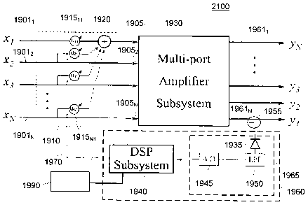
1001591
Figs. 4-18 illustrate the first embodiment of a multi-port self-calibrating
circuit and
related method for distortion compensation of the present invention in
application to quadrature
transmitters. In the following portion of the description we will show that
essentially the same
approach can be used to provide self-calibration capabilities to other multi-
port circuits which
¨31¨
CA 02576778 2007-03-06
16 Doc No: 102-25 CA
Patent
operate on multiple input modulated signals and can have internal mismatches
and imperfections
leading to distortions in output signal or signals.
001601 Accordingly, we will now turn to describing a second embodiment of the
present
invention, wherein the method of the present invention is applied to
calibrating a multi-port
amplifier (MPA), and a self-calibrating MPA is provided.
1001611 A four-port example of a prior-art MPA is shown in Fig. 1 and has been
briefly
described hereinabove according to prior art. From the point of view of
circuit calibration and
compensation for distortions associated with circuit mismatches and
imperfections, a main
difference from the QT 100 described hereinabove is that an MPA has typically
as many output
ports as it has input ports, and the number of input ports typically exceeds
2. In a next difference,
input signals that an MPA receives may be modulated by differing modulation
formats and
therefore have differing reference distribution information associated
therewith and with the
corresponding output signals.
[00162] Before turning to a detailed description of the circuit and method of
the present
invention in this second embodiment, it is instructive to present a
mathematical model of a prior-
art MPA having N input ports and N output ports.
1001631 Referring now to Fig. 19, a simple 2-port MPA 1900 is shown, which
consists of two
preferably identical amplifiers (PAs) 930a and 930b connected between an input
3-dB 90 hybrid
combiner 925a and an output 3-dB 90 hybrid combiner 925b. Hereinafter in this
specification
the 3-dB 90 hybrid combiners, including the 3-dB 90 hybrid combiner 925a,b
will be referred
to as 3-dB couplers.
1001641 In the figure, x1 and x2 denote the two input signals, while yj and y2
denote the two
output signals. The transfer functions of the input and the output couplers
are denoted by an
input and an output matrices H1 and Ho , respectively, as follows:
nil rip.)
H 1 ,
(
(21)
100165] and
-32-
CA 02576778 2007-03-06
Doc No: 102-25 CA
Patent
. in ,
HO =
' 21;22
(22)
1001661 The amplifiers 930a,b are represented by a diagonal matrix
Cl
-
- 2 )
(23)
[00167] with G1 and G2 representing the complex gains of the respective PAs.
The input-
output relationship of the 2-port MPA is characterized by an MPA transmission
matrix T2
T2 = HO X P2 XHI (24)
[00168] In the last equation, the subscripts "2" identifies the number of
input ports of the
MPA, and simultaneously the size of the respective matrix.
1001691 Ideally, the transfer matrix of the 3-dB couplers 925a,b have the
following form:
/ 1.
H = H( ) = , = 7 7
_ -
(25)
[00170] where j = =\i-1 represents a 900 phase shift. If the two PAs 930a,b
have equal gains,
i.e., GI = G2 = G, then the MPA transmission matrix has an anti-diagonal form:
v/72. v7)._ `\ 1 .1/v2
_=
\ vi.7 / vi7 (-; / viT i/\2
(-;
jC
(27)
[00171] Therefore, the transfer function of an ideal 2-port MPA is
characterized by an anti-
diagonal matrix, whose anti-diagonal elements are equal to the PA's gain while
all other
elements are equal to zero. Under this condition, the output signals of the
ideal 2-port MPA are
-33-
CA 02576778 2007-03-06
- Doc No: 102-25 CA
Patent
just scaled, i.e. amplified versions of the input signals, without any added
cross-talk or "leakage"
of any of the input signals into more than one output port:
yi = j=G=xi,
Y2 =/"G -x2 (28)
1001721 Note that the equations (27) and (28) hold due to a perfect mutual
cancellation of
fractions of each of the input signals as they arrive at all but one output
port, due to a particular
balanced form of the 3-dB coupler matrix and the gain equality of all the PAs
of the MPA 1900.
Accordingly, under the ideal conditions, the MPA's output signals are the
amplified versions of
the input signals. Generally, an ideal 2-port MPA provides 2 independent
amplification channels
for the 2 input signals without any cross-talk between said channels. In
practice, however, there
always exist some mismatches and imperfections in the 3dB couplers 925a,b and
the PAs 930a,b.
Therefore, due to non-ideal characteristics of the used components, the MPA
1900 transmission
matrix is in general non-diagonal:
ri, 2 ¨ _itI I t
. 12
,
(29)
\t21 t22/
1001731 and the relationship between the output signals and the input signals
can be presented
in the following matrix form:
(Y2 (t11 t12 YXI\ (t11x1+ t12X2
= = (30)
\.Y1, \..121 122)\x2) t21.X1 + t22X2i
[00174] where
{ tn. = (iii 111G1 + (1.11.112G2
,(-, , > f
i 12 = (L12 ;1 .1.-T.I. -I- ".'"')1.`i"-"
1 rr
t-)1 = '11 21 -1
,. /.
.(=,) = (1 10 Ji.')1("; 1 + ( i.).), ./=-)2(_;=-)
(31)
-34-
CA 02576778 2007-03-06
- Doc No: 102-25 CA
Patent
[00175]
and aii and pu are coefficients of the non-ideal transmission matrices of the
3-dB
couplers 925a and 925b, as shown in Fig. 19, and G, and G2 are the complex
transfer functions
of the first 930a and second 930b PA respectively.
[00176] Equations 30 and 31 demonstrate that in the presence of device
mismatches and
imperfections, the MPA output signals are distorted by cross-talks between the
amplification
channels, or coupling between each input port and a plurality of the output
ports.
[00177] Referring now to Fig. 20, a prior-art 8-port MPA 2000 is shown by way
of example.
Similar to the 2-port MPA shown in Fig. 19 and a 4-port MPA shown in Fig. 1,
the MPA 2000
which consists of an input hybrid matrix (IHM) 2010, a bank of 8 amplifiers
2015, and an output
hybrid matrix (OHM) 2020.
[00178] The IHM 2010 includes three columns 2001, 2003 and 2005 of four 3-dB
couplers
25, connected by two connection networks 2002 and 2004. Similarly, the OHM
2020 includes
three columns 2011, 2013 and 2015 of four 3-dB couplers 25, connected by two
connection
networks 2012 and 2014, wherein the connecting networks 2002, 2012 and 2004,
2014 are pair-
wise identical.
[00179] If all of the 3dB couplers 25 have the same ideal parameters, and all
of the PAs 30
have exactly the same gain and phase delay associated therewith, transmission
characteristics of
the MPA 2000 can be described by an anti-diagonal 8x8 matrix Tg:
0 H II 0 II 0 -j(; \
IIII
0 II II 0 II -.G. ()
.1
II 0 ii ii 0 -J ( ; 0 0
ii u II II ¨"C.; H 0 0
II 0 H -.,.0 0 II 0 0
II 0 ¨JC; II i) II ) 0
II ¨JG ii II 0 II 0 0
0 II If 0 II 0 0 /
(32)
[00180] Accordingly, an ideal 8-port MPA provides 8 independent amplification
channels for
the 8 input signals without any cross-talk between said channels. However, if,
for example, there
-35-
CA 02576778 2007-03-06
Doc No: 102-25 CA
Patent
are internal mismatches and imperfections in at least some of the 3dB couplers
leading to an
imbalance between their output ports, in the MPA transmission matrix appear
non-antidiagonal
elements resulting in cross-talk between the amplification channels and the
undesired cross-
coupling of the output signals, when, for example, an output signal yi from an
output port 2031
includes not only an amplified signal xi received in an input port 2028, but
also traces of one or
more input signals xi, from other input ports.
[00181] In a general case of N-port MPA, where N=211, where q is an integer,
an ideal transfer
matrix TN can be represented as
0 = = = 0 PG\
T
0 PG 0
-
tv - (33)
=
. .
j"G 0 0
N.N
[00182] i.e. again having an anti-diagonal form with all the other elements
of the matrix being
zero, resulting in a desired amplification operation when each of the output
signals yi ,
is an amplified input signal x, , without any cross-talk between the channels.
Here again, this
ideal result is a consequence of a perfect cancellation of fractions of the
input signals arriving at
each output port but one, due to perfectly balanced 3dB couplers and PAs
within the N-port
MPA.
1001831 Accordingly, if transmission characteristics of at least some of
these elements deviate
from the ideal, a transfer matrix of such a non-ideal, or real MPA has non-
diagonal elements and
is representable as a general-form NxN matrix
ti (34(1.V
TN = 121 12:1 t')N
\ tN IIN2 t.VN
-36-
CA 02576778 2007-03-06
Doc No: 102-25 CA
Patent
1001841
wherein at least some of the non-antidiagonal transmission coefficients t,j,
with j#
(N+/-0, are non-zero.
1001851 Turning now to Fig. 21, the second embodiment of the self-calibrating
multi-port
circuit of the present invention 2100 includes an N-port MPA 1930, a
distortion compensation
network 1910, and a feedback circuit 1960. The self-calibrating multi-port
circuit 2100, which is
also referred to hereinbelow as the self-calibrating MPA (SCMPA) circuit 2100
or the SCMPA
2100, receives in operation N input signals xi, i = 1,...,N, in N input ports
19011 to 1901N, and
provides at the output N output signals y,, i = 1,...,N, each of which is
ideally one of the input
signals amplified by a gain coefficient G of the MPA 1930. In an alternative
embodiment, the
number of output ports of the MPA 1930 may differ from the number of input
ports thereof. The
signals xi to be amplified by the SCMPA 2100 are digitally modulated signals
modulated using
same or differing modulation schemes, for example such as M-PSK or M-QAM. As
discussed
hereinabove, such a signal modulated using a given modulation format and a
pulse-shaping
function has a unique statistical distribution, referred to herein as the
reference distribution, such
as the PDF or CDF; according to the method of the present invention, this
reference distribution
is compared to an output distribution for the respective signal as measured as
the output of the
SCMPA 2100 to assess signal distortions introduced by the SCMPA.
1001861 The N-port MPA 1930, which in the context of this embodiment will be
referred to as
the first circuit 1930 or the MPA Subsystem (MPAS) 1930, has N input ports
19051 to 1905N
which are commonly referred to hereinafter as the MPAS input ports 1905, and N
output ports
19611 to 1961N which are commonly referred to hereinafter as the MPAS output
ports 1961.
Counting the input and output ports of the MPAS 1930 from top to bottom as
shown in Fig. 21,
the ports 19051 and 19611 will be referred to hereinafter as the first input
and first output ports of
the MPAS 1930, respectively, while the ports 1905N and 1961N will be referred
to hereinafter as
the Nth input and Nth output ports of the MPAS 1930, respectively. The MPAS
output ports 1961
serve also as the output ports of the SCMPA circuit 2100.
1001871
The distortion compensation network 1910 has N input ports 19011 to 1901N,
which
serve also as input ports of the self-calibrating MPA circuit 2100, and will
be commonly referred
to hereinafter as the circuit input ports 1901. In a preferred embodiment,
each of the circuit input
¨37¨
CA 02576778 2007-03-06
. Doc No: 102-25 CA
Patent
ports 1901 is connected to each of the MPA input ports 1905 using a connecting
link that
includes an externally controllable multiplier 1915ii, for tuning a
transmission coefficient u1, i,j =
1,...,N, of the link 'if. The transmission coefficients u,j, which are
generally complex-valued
and characterized each by an amplitude coefficient and a phase shift, will
also be referred to
hereinafter as scaling coefficients. The notation 'if is used herein to
indicate a connecting link
that couples an i-th circuit input port 1901; with a j-th MPA input port
1905j; when used as a
subscript in notation "tiii", it indicates a transmission coefficient of the
'if link, i.e. the link
coupling an i-th circuit input port 1901, with a j-th MPA input port 1905j.
Transmission
coefficients ti,j with
will also be referred to herein as cross-coupling coefficients, as they
couple a controlled fraction of an input signal x1 into a j-th MPA input port
1905j, resulting in a
cross-talk between signals received into the MPA 1910 through different MPA
input ports 1905.
In the preferred embodiment, each of the MPAS input ports 1905 receive a
modified input
signal which is representable as a linear combination of the N input signals
xi, i=1,...,N.
1001881 The feedback circuit 1960 includes a processor 1940 that can be
embodied as a DSP,
and a sampling circuit 1965 connected between one of the output ports 1961 and
the DSP 1940.
The sampling circuit 1965 can be functionally and structurally substantially
identical to the
sampling circuit 255 of the first embodiment and is described hereinabove with
reference to Fig.
4; it includes a tap-off coupler 1955, an envelope detector 1935, and anti-
aliasing LPF 1950 and
an AID 1945. As shown in Fig. 21 by way of example, the sampling circuit 1965
is coupled to
the N-th output port 1961N, and cooperates with the DSP 1940 for monitoring
the output signal
yi from said output port 1961N-
100189]
The DSP 1940 is linked to the distortion compensation network 1910 by one or
more
control links exemplified in Fig. 21 by a bus 1970, and in operation generates
signals for
controlling the multipliers 1915ii to adjust complex transmission coefficients
uij of the connecting
links 'if within the compensation circuit 1910. Similarly to the operation of
the DSP 245 of the
first embodiment, the DSP 1940 is programmed to perform the following
operations:
1001901
a) determines output distribution information for the output signal yi(t) from
a
plurality of samples {p'} of the output signal yi, said plurality of samples
{p,} provided by the
sampling circuit 1965,
-38-
CA 02576778 2007-03-06
. Doc No: 102-25 CA
Patent
1001911 b) compares the output distribution information with a respective
reference
distribution information for the monitored output signal yl which is stored in
a memory 1990,
and
1001921
c) determines therefrom distortion compensation information for setting the
complex
transmission coefficients uu so as to reduce a difference between the
reference and output
distribution information; this difference is reduced by the addition of a
controlled amount of
cross-coupling and cross-correlation between the signals input into the ports
of the MPAS 1930
so as to compensate for the undesired imbalances and cross-coupling
therewithin the first circuit
1930, thereby reducing the cross-talk between the amplification channels
appearing at the output
channels of the self-calibrating MPA circuit.
[00193]
Fig. 21 shows one sampling circuit 1965 for monitoring output from one, i.e. N-
th, of
the N output ports 1961, and a corresponding portion of the distortion
compensation network
1910 which is responsible for modifying only a signal that is provided to the
first input port
19051 of the MPAS 1930; it includes a set of N multipliers 1915u=i with
corresponding cross-
connecting links 'ii' coupling each of the input signals x1 into the first
input port of the MPAS
1930. The shown elements are sufficient to substantially compensate
distortions that the MPAS
circuit 1930 introduces to the output signal yi. However, it may also in the
process additionally
distort the other (N-1) output signals .)),, i=2,...,N, if those signals are
not monitored. In a
preferred embodiment, the feedback circuit 1960 includes N sampling circuits
such as the
sampling circuit 1965, each coupled to a different one of the N output ports
1961 so as to
monitor each of the output signals yi, i = 1,...,N, of the self-calibrating
MPA circuit 2100,
providing to the DSP 1940 N pluralities of signal samples {N}. The DSP 1940
processes the
received pluralities of signal samples to determine output distribution
information for each of the
N output signals, and compare the output distribution information for each of
the output N output
signals y, with reference distribution information for the respective output
channel. In another
embodiment, the single sampling circuit 1965 is used sequentially to gather
the signal power
distribution at each output port 1961, i.e. one after the other, for example
using an Nxl switch
connected between the output ports 1961 and the sampling circuit 1965. In yet
another
embodiment, one or more of the input signals x, includes frequency-multiplexed
modulated
channels and the feedback circuit 1960 processes these channels as a single
one, using reference
-39-
CA 02576778 2007-03-06
=
Doc No: 102-25 CA Patent
distribution information representing statistical characteristics of the
multiplexed signal without
distortions.
1001941 If each of the input signals xi has the same modulation format and
same pulse shape,
only one reference distribution information, such as the PDF or the CDF, needs
to be stored in
the memory 1990. Otherwise, different reference distribution information
should be provided for
each different modulation format/pulse shaping function combination, so that
the memory 1990
may store a plurality of reference distributions corresponding to a plurality
of modulation and
pulse shaping formats.
1001951 Alternatively, the modulation format of each of the N input signals xi
can be
determined in operation by providing to the DSP 1940 samples of the input
signals xi, e.g. using
sampling circuits similar to circuit 1965 but coupled to the input ports 1901,
and programming
the DSP 1940 to determine therefrom input signal envelope distributions to use
as the reference
distributions for the respective output signals. In one such embodiment, the
sampling circuit
1965 can be time shared, e.g. switched between the input 1901 and output 1961
ports to tap off
and sample the respective input and output signal alternately.
1001961 Before describing the operation of the SCMPA 2100 in further detail,
it is instructive
to provide several mathematical notations and formulas representing the SCMPA
operation in
mathematical terms.
1001971 Denote the plurality of input signals with a vector X, the
plurality of output signals
with a vector Y, and the plurality of transmission coefficients uu with a
matrix U, hereinafter
referred to as the compensation matrix:
./.1 iii) === Hi\ \ / 11\ \
11,1 1,22 = = = 1/ ,\ !I\
x = . u . and Y =
"II ) = = = if :fIl
(35)
[00198] With these notations, the operation of the SCMPA 2100 is described
by the
following matrix equation:
-40-
CA 02576778 2007-03-06
, Doc No: 102-25 CA
Patent
Y = T\UX (36)
1001991
Equations (36) and (35) result in a following formula (37) for an n-th output
signal }In,
n=1,. ..,N:
= =ill
till ill õ )=i.õ + ( tõ./,
/.I / I, I / õ /.. (37)
1002001
One can see that the last term in the RHS of equation (37) represents signal
cross-talk
at the n-th output port 1961, and should be minimized or, preferably,
eliminated. This is
possible by selecting the transmission coefficients u, i,j = 1,...,N, of the
connecting links in the
compensation network 1910 so that
-- Ii
=1 (38).
1002011
The process of selecting such values of the transmission coefficients uji ,i,j
= 1,...,N,
that satisfy the equation (38) so as to compensate for the imbalances in the
first circuit 1930
thereby providing for cross-talk-free output, will be referred to as
calibration of the SCMPA
2100. This is done in the present invention by iteratively adjusting the
transmission coefficients
uu so as to reduce an objective function representing distortions of the
output signals statistics.
1002021 For this purpose, the DSP 1940 computes for each of the output signals
yi an output
PDFnactuai(m) from the respective plurality of L signal samples {P}L, and then
compares it with a
corresponding reference distribution PDFnideai(m) stored in the memory 1990.
In one
embodiment, N objective functions can be formed for each output signal using a
measure of
differences between the respective reference and output distributions, which
can then iteratively
be minimized one by one for each of the output signals individually, similarly
to how it is
described hereinabove for the first embodiment. Advantageously, an embodiment
described
hereinbelow employs a single objective function combining together distortions
of output signal
statistics in a single error function
-41-
CA 02576778 2007-03-06
Doc No: 102-25 CA
Patent
= E ,
pay!: (,,, ,
(39)
1002031 where
(iii)
(40)
1002041 denotes the PDF mean-squared error (MSE) for the output signal at an n-
th output
port 1961. Alternatively, other measures of PDF difference may also be used.
In another
alternative embodiment, respective CDFs can be used in place of the PDFs to
assess the circuit-
induced distortion of statistical properties of the output signal and to
compute the objective
function, as described hereinabove with reference to the self-calibrating QT
200.
1002051
In accordance with the invention, the compensation circuit 1910 is tuned
during
normal operation of the SCMPA 2100, by iteratively adjusting the transmission
coefficients
forming the compensation matrix U so as to minimize the objective function -µ
I ), which has a
minimum when equation (27) is satisfied, and the output signals y, have
statistical distributions
approximating the respective reference distributions of un-distorted modulated
signals.
Mathematically, the circuit calibration process can be expressed as finding a
minimum of the
objective function
vµ"
itilti õ ,,,,,, ,)-}
(41)
1002061 By solving this minimization problem, we achieve the purpose of
calibrating the N-
port MPA. To this end, many approaches can be used. Examples are the alternate
1-dimensional
search described hereinabove, and the method of steepest descent.
¨42¨
CA 02576778 2007-03-06
Doc No: 102-25 CA
Patent
[002071 An embodiment of the iterative circuit calibration method according to
the present
invention that employs the method of steepest descent will be now described.
The method of
steepest descent is one of the oldest methods of optimization, and is well
know to those skilled in
the art. It employs an iterative procedure to search for the minimum of an
objective function of
many variables. At each iteration, a direction of the steepest descent from
the current position on
the surface of the objective function is found, and the operating point is
moved along this
direction to a next position, resulting in a smaller value of the objective
function.
1002081 Mathematically, the direction of the steepest descent is defined by
a gradient vector
Di = V.A4 (V/ )
1002091 and the updating process is described by the following equation:
Ut i = (It ¨ AtD1
1002101 where the subscript "t" denotes the time index, Dt denotes the
matrix of derivatives of
M(U) with respect to U at time "t". Xt represents the step size of the
adjustment, and its subscript
"t" implies that its value may be adjusted over time.
1002111 Intuitively, the successive updates or corrections to the
calibration matrix U in the
direction of the negative gradient, i.e., the direction of the steepest
descent, should eventually
lead to the minimum value of the objective function M(U), at which point the
calibration matrix
U reaches its optimum value. As an illustration, arrows 2210, 2220 and 2230 in
Fig. 22 show the
search path on a plane of two parameters for three consecutive steps of the
steepest descent for
the case of a two-port MPA, when it is sufficient to adjust only one complex
cross-coupling
coefficient u12.
1002121 Turning now to Fig. 23, an implementation of the method for distortion
compensation
of the present invention for the SCMPA 2100 using the steepest descent
algorithm to tune the
compensation circuit 1910 will now be described. This figure shows a flowchart
of the
calibration process. It includes four major sub-processes, or steps:
Initialization step 2310,
determining compensation information step 2340, which takes the form of
Determining Matrix
-43-
CA 02576778 2007-03-06
Doc No: 102-25 CA
Patent
of Derivatives as labeled in Fig. 23 and explained hereinbelow, Calibration
Matrix Update step
2350, and Modifying the Compensation circuit step 2360. These steps are
described
hereinbelow.
[00213] During the initialization step 2310, the following operations are
performed:
[00214] A) the reference PDFs for the N output signals, PDF (m) (M
nideal
1, 2, = = = ,M) for
given modulation schemes and pulse-shaping functions of the MPA input signals
xn are loaded
from the memory 1990, computed or determined by measurements;
[00215] B) the compensation matrix U is initialized as follows: U=U0,
t_ =
=
= = = J
= \ = \
[00216] and the matrix Uo is uploaded to the compensation circuit 1910;
[00217] C) N sets of signals samples {s}L is acquired as described
hereinabove, each of which
consisting of L samples and taken from one of the MPA output ports 1961 using
sampling
circuits such as the sampling circuits 1965.
[00218] D) N output distributions are determined in the form of
PDFnactuat(m), = 1, 2, = = =
,B) from the N sets of signals samples Isnl, each for a different output
signal yn;
[00219] E) Compute the objective function M(U) using the current compensation
matrix, for
example using equation (39).
1002201 The step 2340 of determining the compensation information involves
determining the
direction of the steepest decent to the minimum of the objective function,
i.e. the calculation of
the gradient vector D. It includes performing the following sub-steps for each
cross-coupling
coefficient ujk:
1002211 increment ttik by a small pre-defined step 6,
-44-
CA 02576778 2007-03-06
, Doc No: 102-25 CA
Patent
1002221 perform sub-steps (C)-(E) as described hereinabove with reference
to the initialization
step 2310;
[002231 compute a derivative parameter dik using the following equation
(42):
¨(.111(7.1 ¨
(42)
[002241 Performing the above defined sub-steps for each cross-coupling
coefficient uii, results
in a gradient matrix
(IP 013 = = = (II
4121 1) J23 = = = (i.)A-
D = =
\ (I A- '/A2 (I;\3 = = = 0 )
(43)
[002251 In the next step 2350, each of the cross-coupling coefficients uik
is updated according
to the following update equation:
[002261 ttik(t+1) = ujk(t) dik
1002271 where ujk(t) denotes the cross-coupling coefficient uik at time
index t prior to
performing the step 2340. At the end of step 2360, thereby updated
compensation matrix U(t+1)
is uploaded to the compensation circuit 1910, and the transmissions of the
connecting links 'if' is
adjusted accordingly. The process iterates until a pre-determined condition is
met, for example,
until the objective function reaches a pre-determined threshold value.
1002281 The overall performance of the aforedescribed circuit calibration
process depends on
a number of process parameters, optimal values of which should be determined
depending on
particular application requirements, as would be known to those skilled in the
art.
1002291 For example, the number of samples L and the bin size used in the PDF
calculation
need to be chosen properly. To achieve accurate distortion compensation, a
large sample size
¨45¨
CA 02576778 2007-03-06
Doc No: 102-25 CA
Patent
should be used. The bin size and locations also affect the performance, and an
optimal choice of
the bin size depends on the sample size.
[00230] Two other important parameters are 5 for the gradient matrix
calculation, and 2 for
the compensation matrix update. Their values control the convergence rate and
the steady-state
performance, where large values result in a faster convergence rate at the
expense of the steady-
state performance. Variable values of 6 and A, may be used to alleviate these
issues.
[00231] The above described procedure does not update the diagonal elements
Ili; of the
compensation matrix U. These diagonal elements control the output powers of
the SCMPA 2100,
and they can be adjusted separately by directly monitoring the output signal
powers, and
updating the scaling coefficients uil accordingly. This approach reduces the
number of degrees of
freedom in the optimization, and simplifies the computational requirements.
SCMPA Simulation Results
1002321 The perfomiance of the aforedescribed SCMPA 2100 and of the related
method for
distortion compensation in MPA circuit has been verified in simulations. By
way of example,
computer simulations have been preformed for a 4-port MPA whose co-channel
input signals are
as follows:
[00233] Port 1: QPSK modulation, Square-root raised-cosine pulse-shaping, Roll
off= 0.35.
1002341 Port 2: QPSK modulation, Square-root raised-cosine pulse-shaping,
Roll off= 0.25.
[00235] Port 3: 8-PSK modulation, Square-root raised-cosine pulse-shaping,
Roll off= 0.35.
[00236] Port 4: 16-QAM modulation, Square-root raised-cosine pulse-shaping,
Roll off --
0.35.
1002371 Without loss of generality, these signals are normalized to a power of
1 at the input to
the calibration circuit.
[00238] It is assumed that the 3-dB 90 hybrid combiners in the input and
output sections of
the MPA have a gain error within +/-1dB and a phase error within +/-10degrees;
the PAs have a
-46-
CA 02576778 2007-03-06
=
Doc No: 102-25 CA Patent
gain variation within +/-1dB and a phase variation within +/-10degrees; and
the hybrids in the
output section have a gain error within +/-1dB and a phase error of +/-
10degrees. These errors
are generated from a uniform random number generator. The resulting total
transfer function of
the MPA used in the simulation is listed in Table 2.
Tz11,1(,,, 2: T11(.= total trati4,..r function generated for simulations
Amplitude (dB) Phase (Degree)
-15.0 -17.S -17.6 0.3 -149.7 -9.1 -122.4 -1.3
-90.4 -15.7 -0.-1 -22.8 -16.1 25.0 -13.6 -112.6
0.9 -19.1 -14.9 -174.2 11.3 -62.5 173.2
0.0 -26.5 -16.0 -18.7 0.0 -87.3 167.1 95.7
1002391
In the PDF calculation, thirty-one bins are used, located at bi = 0.1(j - 1),
(1= 1, 2, = = =
, 31). The parameter 6 is set to 0.01 to calculate the gradient matrix Dt, and
a fixed step size X --
0.01 is used for the calibration matrix update. Two sample sizes, 105 and 106,
are used in the
calculation.
[002401 The following results show the effectiveness of the aforedescribed MPA
self-
calibration technique: the PDFs without/with calibration, the convergence
performance, the
isolation improvement, and the received signal constellation.
1002411 Figures 24 and 25, for sample size 105 and 106 respectively, show four
sets of PDFs
each. Each set has three curves, wherein solid curves represent the ideal, or
reference PDF,
dashed curves represent the MPA output PDF without calibration, and the dotted
curves
represent the MPA output PDF with calibration. In this example, 100 iterations
are performed.
The PDFs calculated at the first and the last iterations are plotted as the
ones without calibration
and with calibration, respectively. It is observed that the self-calibration
indeed restores all PDFs
to their ideal ones.
[00242] At the end of the simulation, the improvement in isolation between
the four ports are
calculated, and the results are listed in Table 3 for both sample sizes. The
first 4 columns in the
table are the MPA's amplitude transfer functions from Table 2, listed as
reference. The second 4
columns list the combined amplitude transfer functions of the MPA and the
calibration circuit.
-47-
CA 02576778 2007-03-06
=
Doc No: 102-25 CA Patent
The last 4 columns show the differences between them, i.e., the isolation
improvement due to the
aforedescribed self-calibration technique of the present invention. It shows
that using the self-
calibration technique, the isolation between the ports are reduced at least to
-31dB with the
sample size of 105, and to -33dB with the sample size of 106. Depending on the
original isolation,
the improvement can be as large as 29dB.
[00243]
Fig. 26 illustrates that the method converged within 50 iterations, yielding a
smaller
residual error for the larger set of samples.
[00244]
Figs. 27-30 illustrate output signal constellations before (left panes) and
after (right
panes) the calibration process for the sample size 105. The figures also
indicate at the top the
signal-to-interference ratio (SIR) as the performance measure. These figures
clearly show the
signal constellation degradation due to the cross channel interference caused
by the MPA
imperfections. They also show that the self-calibration technique
significantly reduces the cross
Table 3: Jcclaf It n 11011)1'01,1.1111Df-: in dB) achieved by the self-
calibration technique
x if
linpn weinent
Sample size =
-15.0 -17.8 -17.6 0.3 -31.8 -33.3 -36.2 -0.008 16.8 15.5 18.6 0.3
-20,1 -15,7 -0.4 -99. -35,0 -37,5 -0.005 -39.5
1-1.6 21.8 -0.4 16.7
-25.2 0.9 -19.1 -14.9 -35.8 -0.008 -32.0 -37.3
13.6 0.9 19.9 92.5
0.0 -26.5 -16.0 -18.7 -0.005 -43.7 -37.7 -36.9 0.0 17.2 21.7 18.2
Sample size = 101'
2 -39.2 -34.7 -0.005 18.2 91.5 17.0 0.3
the saint:. a. -39.0 -36.0 -0.002 -35.4 18.6
21.2 -0.4 12.6
above -46.4 -0,000 -48.1
-53.0 21.2 0.9 29.0 3,8.1
-0.001 -41.9 -43.0 -43.7 0,0 15.4 27.0 25.0
Vable
Sib's before and after the self-calibration. Values in bracket are
imprcovenit:snt.
After (dB)
Port= Before (dB) Sample size = 10ri Sample size = 106
1 14.6 34.2 (19.6) 38.3 (23.7)
14,7 30.5 (15.8) 36.5 ( 21.8 )
3 12.7 30.7 (18.0) 31.5 (18.5)
4 13.0 28.9 (15.9) 30.4 (17.4)
-48-
CA 02576778 2007-03-06
=
Doc No: 102-25 CA Patent
channel interference and restores the signal constellations, resulting in
significant SIR
improvements as summarized in Table 4.
Third Embodiment: Self-Calibrating Beam Forming Network (SCBFN)
1002451 Another example of a multi-port circuit operating on a plurality of
modulated input
signals to produce a plurality of output modulated signals is a Beam Forming
Network (BFN),
which is commonly used in wireless communication.
1002461
Fig. 31 schematically shows a prior art BFN circuit 3100 in a receive mode of
operation. Each of the N antenna elements 3101 receives incoming wireless
signals from a
plurality of sources located in different directions and at different
distances from the BFN circuit
3100, so that signals received by different antenna elements 3101 from a
particular source differ
in phase and amplitude depending on the directions of the incoming signals. A
signal received
by each antenna element is passed through respective front-end antenna
circuits 3125; where it
undergoes filtering, amplification and optionally frequency conversion in one
or more frequency
conversion stages. Resulting signals form input signals for a BFN sub-circuit
3130, wherein they
are each first split into M split-off signals by 1xM splitters 3111, where
[00247] Each of the M outputs of each of the N splitters is coupled into one
of M signal
combiners/adders 3120 using a connecting link so as to form M output signals.
The connecting
links include multipliers 3115 which impose complex weighting coefficient Wnin
= m =
1,...,M, n=1,...,N on respective signals individually providing pre-selected
amplitude weighting
and phase shifting to said signals.
[00248] The weight coefficients Wõ,õ are selected so as to improve reception
directivity of the
BFN 3100 with respect to a wireless signal received or transmitted from a
particular wireless
source, as compared to reception directivity provided by each individual
antenna element 3101.
With the M sets of weights, M different receive directivity patterns, also
referred to as receive
beams, can be formed, corresponding to the M output signals.
-49-
CA 02576778 2007-03-06
. Doc No: 102-25 CA
Patent
1002491
In practice, the front-end antenna circuits 3125 may have gain and phase
transfer
functions that differ from one to another. In addition, these transfer
functions may vary over
time and temperature. If the weighting factors Wõ have been selected without
accounting for
the real parameters of the front-end antenna circuits 3125 associated with
each antenna element
3101, any mismatch in the gain and phase transfer functions between them will
result in a
distorted directivity pattern, characterized for example by a reduced gain,
skewed directivity,
higher side-lobe levels, etc. There is thus a need to compensate for the
circuit imperfections and
imbalances in the front-end antenna circuits 3125 and the BFN sub-circuit
3130.
1002501 These distortions in the BFN 3100 resulting from internal mismatches
and component
parameter variations can be compensated using another embodiment of the method
of the present
invention, which will now be described with reference to Fig. 32 showing one
possible
configuration of a self-calibrating BFN (SCBFN) implementing the method.
[00251] The SCBFN 3200 includes a BFN sub-circuit 3230 and a feedback circuit
3260,
which is structurally and functionally similar to the feedback circuits 1960
and 250 described
hereinabove, and includes a DSP 3240 coupled to receive output signal samples
from a sampling
circuit 3265.
1002521
Antenna elements and their respective receive chains as shown in Fig. 31 are
not
shown in Fig. 32 so as not to obscure important features of the invention, as
said elements are not
affected by the modifications of the present invention in this embodiment
thereof. They are
nevertheless a part of the SCBFN circuit 3200, which compensates for
distortions within said
antenna and front-end antenna circuits elements that are not shown in Fig. 32.
100253] The BFN sub-circuit 3230 is similar to the prior-art BFN sub-circuit
3130 shown in
Fig. 31 and includes all the elements thereof. It receives the N modified
signals from respective
front-end antenna circuits 3125 as shown in Fig. 31; these N modified signals
are originated from
the N input signals received by the N antenna elements 3101, which can be
considered as the
input ports of the SCBFN 3200. The BFN sub-circuit 3230 has M output ports for
outputting M
output, or beam signals. However, for clarity only one of the M output ports,
which is labeled
'3261', that outputs the beam signal #1 is shown in Fig. 32. Also for clarity,
only a portion of
the BFN sub-circuit 3230 that forms the beam signal #1 is shown.
-50-
CA 02576778 2007-03-06
Doc No: 102-25 CA
Patent
[00254]
As shown in Fig. 32, the feedback circuit 3260 is for compensating the circuit
distortions affecting only the first output signal, labeled as "Beam #1
signals", by adjusting the
respective weighting coefficients W, for m=1 indicating the output port or
signal.
1002551
According to the invention, the multipliers 3115 are controlled by the DSP
3240,
which in operation provides signals via a bus 3230 to adjust the weighting
coefficients W111,
n=1,.. .,N so as to minimize a difference between output statistical
distribution information, e.g.
the output PDF or CDF, obtained from power samples of one of the output
signals of the BFN
sub-circuit 3230, and a respective reference distribution information for said
output signal stored
in a memory 3290. This can be done iteratively using, for example, the
steepest descent
algorithm as described hereinabove with reference to the SCMPA 2100.
[00256] One difference between the SCMPA and SCBFN embodiments, is that in the
case of
the SCBFN, the output signals can be distortion-compensated independently from
each other on
per-output-signal basis, by iteratively minimizing M differences between
respective reference
and output PDFs or CDFs, one for each output signal. This can be done using M
separate
feedback circuits 3260, one per output signal, optionally sharing the DSP
3240, or switching a
single sampling circuit 3265 between the M output ports, and using the bus
3270 to control each
of the MN multipliers 3115.
[00257] Note also, that in the shown embodiment, the SCBFN 3200 does not have
a distortion
compensation network that is added to a functional device for compensating its
internal
imbalances, such as compensation networks 1910 and 210, which compensate for
distortions in
the MPA 1930 and QT 100 but are distinct therefrom.
[00258] Generally, for distortion compensation in a self-calibrating multi-
port circuit
according to the present invention, a variable coupling means is to be
provided for adding a
controlled amount of cross-correlation between at least some of the N input
signals, or signals
originated therefrom within the circuit; in operation, the controlled amount
of cross-correlation is
adjusted by tuning the variable coupling means using a feedback circuit so as
to minimize a
difference between an output statistical characteristic of the actual output
signal and a reference
statistical characteristic for the output signal. A distinct distortion
compensation network is only
one possible embodiment of such variable coupling means, and in other
embodiments the
¨51¨
CA 02576778 2007-03-06
=
Doc No: 102-25 CA Patent
variable coupling means can be provided within a portion of the self-
calibrating circuit that
performs another useful function of the circuit. The self-calibrating circuit
shown in Fig. 32
represents such an embodiment of the invention, wherein the variable coupling
means is formed
using the plurality of adjustable multipliers 3115, which can be tuned so as
to vary relative
amplitudes and phases of the N modified antenna signals received by the N
splitters 3111,
thereby controlling a desired amount of cross-correlation among signals
received by the antenna
elements 3101, so as to improve the directivity.
1-002591 It should be understood that each of the preceding embodiments of the
present
invention may utilize a portion of another embodiment. For example, it is
known in the art to
combine a BFN with an MPA. Examples of such combinations, with the BFN
operating in
receive or transmit modes, are described in US patent 5,936,592. With this
combination of MPA
and BFN, the type-based calibration technique of the present invention can be
applied to
calibrate either the MPA and BFN coefficients jointly or separately one after
the other. In one
embodiment, a SCBFN circuit as described hereinabove can be used for
compensating the circuit
imperfections in the connected MPA,
1002601 Although the self-calibrating BFN was described herein in the receive
mode,
substantially the same circuit configuration and the same method of circuit
calibration with only
minor modifications can be used for the BFN in a transmit mode.
[00261] Advantageously, the aforedescribed method of the present invention for
calibrating
multi-port circuits based on the envelope distortion statistics of the output
signal or signals can
be used during normal operation of the circuit thus allowing it to adapt to
changing conditions
without service interruptions, sampling rate is independent of the signal
bandwidth, does not
require synchronization with the transmitted signals, can work over a wide
range of component
distortions, thus permitting the use of low cost and poor performing devices,
and requires only a
simple diode-based power sampling circuit without high-speed analog hardware.
[00262] Of course numerous other embodiments may be envisioned without
departing from
the scope of the invention. For example, an embodiment of the self-calibrating
MPA is easily
envisioned which does not include a distinct distortion compensation network,
but instead
employs tunable 3dB couplers having externally adjustable amplitude and phase
shift parameters
-52-
CA 02576778 2007-03-06
Doc No: 102-25 CA
Patent
associated therewith, and wherein a type-based feedback is used to directly
adjust said coupling
amplitude and phase shift parameters of at least some or all of the tunable 3-
dB couplers within
the MPA circuit.
¨53¨